
 Open Access Article
 This Open Access Article is licensed under a Creative Commons Attribution-Non Commercial 3.0 Unported Licence
Electrically controlled topological micro cargo transportation†
A. S.
Bhadwal
 a,
N. J.
Mottram
b,
A.
Saxena
a,
I. C.
Sage
a and
C. V.
Brown
*a
a,
N. J.
Mottram
b,
A.
Saxena
a,
I. C.
Sage
a and
C. V.
Brown
*a
aSOFT Group, School of Science and Technology, Nottingham Trent University, Nottingham NG11 8NS, UK. E-mail: carl.brown@ntu.ac.uk
bDepartment of Mathematics and Statistics, University of Strathclyde, Glasgow G1 1XH, UK
First published on 24th February 2020
Abstract
We demonstrate electrically controlled linear translation and precision positioning of a colloidal particle in a soft matter device. The basis of transportation is the time dependent electric field reconfiguration and manipulation of a topological line defect between two distinct hybrid aligned nematic liquid crystal domains having opposing tilt orientations. Deliberately tuning an applied voltage relative to a low threshold value (5.7 V at 1 kHz) permits defect trapping of the colloidal particle and allows subsequent control over the particle's velocity and bidirectional linear movement over millimeter distances, without the need for externally imposed flow nor for lateral confining walls.
1 Introduction
Transport of micrometer sized solid particles, liquid droplets or biological structures in carrier fluid systems is important in a diverse range of disciplines and applications including drug delivery, active matter, and lab-on-a-chip applications.1 There has been intense recent interest in using anisotropic carrier fluids such as nematic liquid crystals2–4 which offer a wide toolkit of potential particle manipulation techniques based on physical (voltage, light, temperature, flow), chemical (surface alignment, photoresponse, phase change), and geometrical (confinement, texturing and patterning) mechanisms. Some recent work includes nematic based micro cargo transportation and manipulation by electrophoresis and electrohydrodynamic convection utilising the asymmetric nematic distortions around an embedded particle,5,6 by phase boundary movement of a particle trapped on a defect formed within a microgroove,7 by flow within a microchannel with the particle trapped on a “soft rail” defect,8 and by spatial gradients in the elastic distortion of the nematic produced via patterned substrate morphologies, via textured periodic surface alignment on the substrate or via periodic patterning of the lateral walls of a confining channel.9–11With long term goal of designing soft matter electronic devices, we report an electrically controllable micro cargo transportation device that employs a topological defect in a flat nematic liquid crystal layer for particle trapping and manipulation. Liquid crystals exhibit a range of different topological defects including monopoles and lines which can be embedded within textures and at domain walls12,13 and which arise in general as a consequence of frustration and symmetry breaking in the system caused by geometric spatial confinement, alignment, and surface anchoring, electrostatic or magnetic confinement, and flow alignment.14,15 Topological defects inevitably arise in the nematic director field surrounding a suspended micrometer scale colloidal particle.2,16 We have used hybrid alignment of a nematic layer to create two stable coexisting equilibrium n-director tilt orientations which are separated by an elastic domain wall that contains a line defect. Previous work on the formation17 of a topological defect line and its structural transformation18–20 under hybrid alignment conditions has been reported for confinement in thin microchannels.
Here we use electrical confinement of the domain wall between opposing hybrid alignment states, without lateral confinement, to significantly distort the shapes of the domains and manipulate the domain wall to evolve a series of parallel intervening walls connected by high curvature tip regions. We have developed a nematic continuum theory model that duplicates the observed time evolution of the tortuous shape of the wall and which quantitatively reproduces the A.C. voltage controlled linear motion of the tip in the low-velocity range. We have used this high curvature tip feature on the electric field confined domain wall to collect, trap and move a micro particle. This provides straightforward precision A.C. voltage control of the positive and negative linear movement and placement of the particle, without any need for externally imposed flow, nor for lateral confining walls or geometric or alignment texturing.
2 Experimental
2.1 Device details and preparation
The device consisted of a nematic liquid crystal layer of thickness d = 13 μm sandwiched between two borosilicate glass substrates in the xy plane, Fig. 1. The lower substrate at z = 0 was patterned with an array of transparent co-planar interdigital stripe electrodes running parallel to the x-direction. The lower substrate was coated with a thin solid film which imparted low-pretilt planar nematic surface alignment with the easy alignment axis in the y-direction, orthogonal to the direction of the electrode lines. The opposing upper substrate at z = d was coated with the amorphous fluorinated copolymer Teflon AF (“PTFE AF 2400”, poly[4,5-difluoro-2,2-bis(trifluoromethyl)-1,3-dioxole-co-tetrafluoroethylene], dioxole 87 mol%), CAS 37626-13-4, Sigma-Aldrich/Merck KGaA, Darmstadt, Germany which imparted homeotropic nematic surface alignment (see also Supplementary file F1, ESI†).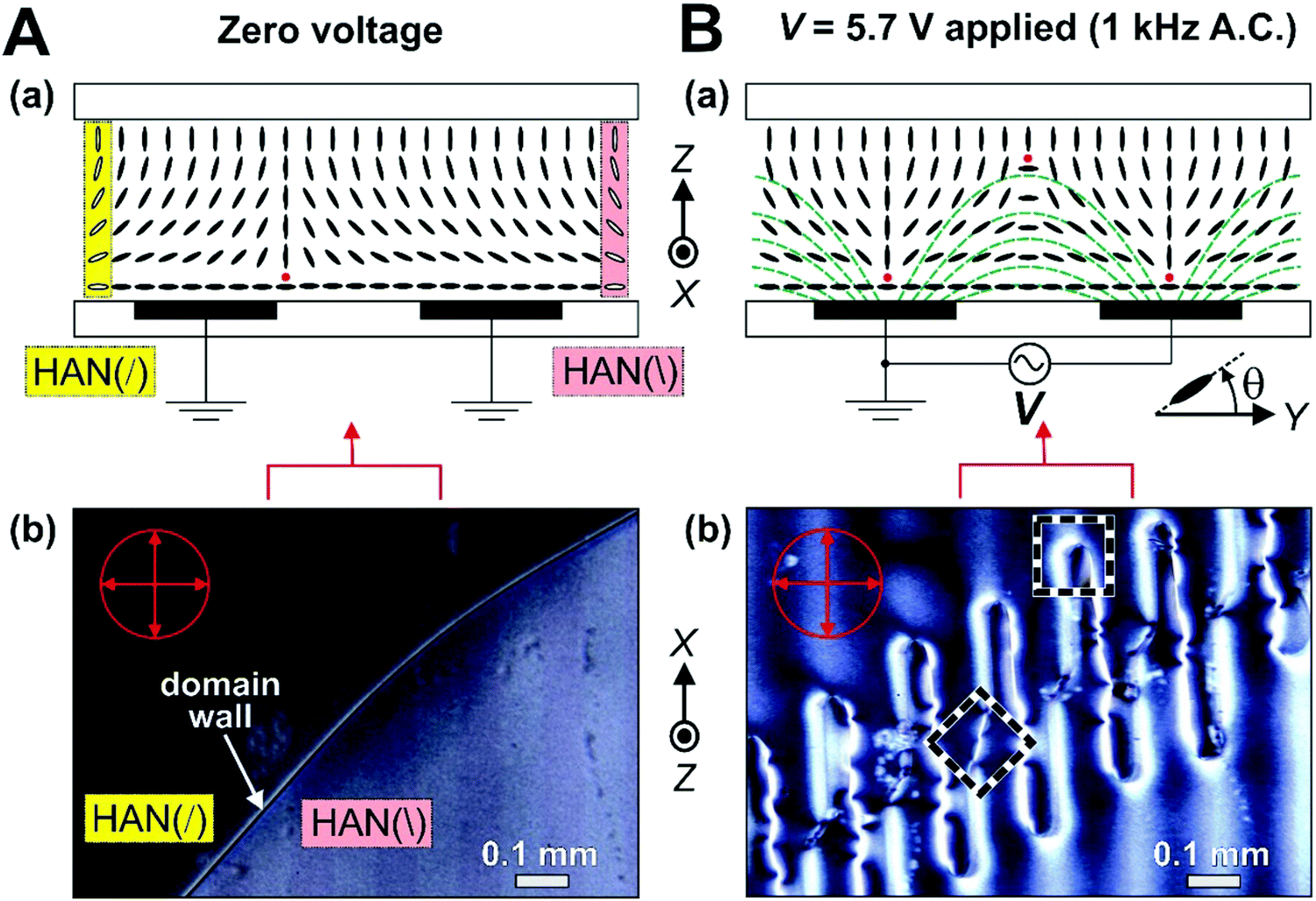 | ||
| Fig. 1 (A) The nematic layer with no applied voltage: (a) illustration of the orientation of the nematic n-director in cross-section showing the coexisting HAN(/) and HAN(\) alignment states separated by a domain wall containing a topological line defect of strength −½ (note that the location of the line defect, the red dot, is arbitrary in the zero voltage state), (b) optical micrograph of the actual device under plane-polarised light with a crossed analyser showing two coexisting HAN regions separated by a diagonal domain wall. (B) The nematic layer under an applied voltage V, producing electrical confinement: (a) illustrating the nematic n-director configuration with the domain wall moved into the gap region between the electrodes. (b) The optical micrograph shows that electrical confinement has produced a tortuous domain wall shape with intercalated electric field distorted HAN(/) and HAN(\) regions. The crossed polariser and analyser orientations are shown by the arrows in the circle on the micrographs. | ||
The electrodes on the lower substrate were fabricated on indium tin oxide coated borosilicate glass slides using standard photolithography and etching techniques (ITO of 25 nm thickness and 100 Ω per square resistivity, Praezisions Glass and Optick GmbH, Germany). The electrode arrangement covered a square area of size 5 mm × 5 mm, whilst the electrode linewidth and the gaps between the electrodes were both equal to we = wg = 80 μm. The entire lower substrate was coated with a magnesium fluoride on zinc sulphide mechanical alignment layer with a combined thickness of 300 nm. The magnesium fluoride layer was deposited with the plane of the substrate tilted at 45° to the evaporation direction. This provided mechanical nano-groove planar alignment of the nematic liquid crystal with a negligible pretilt angle.21 Inorganic thin solid films, for example silicon dioxide and associated solid dielectrics, commonly provide a polar anchoring energy of the order of 10−5 J m−2![[thin space (1/6-em)]](https://www.rsc.org/images/entities/char_2009.gif) 22 similar to conventional polyimide23 and polyvinyl alcohol alignment layers.24 Magnesium fluoride thin films have previously been used to align twisted nematic cells in the literature, giving a comparable electro-optical performance to polyimide alignment layers.21
22 similar to conventional polyimide23 and polyvinyl alcohol alignment layers.24 Magnesium fluoride thin films have previously been used to align twisted nematic cells in the literature, giving a comparable electro-optical performance to polyimide alignment layers.21
We used nematic liquid crystal material E1, which has a density of 1.01 ± 0.01 g cm−325,26 and which is a two component mixture of 5CB and 7CB (4′-pentyl-4-biphenylcarbonitrile, CAS 40817-08-1, and 4′-heptyl-4-biphenylcarbonitrile, CAS 41122-71-8, Sigma-Aldrich/Merck KGaA, Darmstadt, Germany) in the proportion 60%:40% by weight. This mixture exhibits a stable room temperature nematic phase, and the mixture and its cyano-biphenyl components27,28 are established and well characterised materials. We measured the value of the positive dielectric anisotropy, Δε = 12.3 ± 0.4, and also the values of the splay and bend elastic constants, K11 = 7.2 ± 0.5 pN and K33 = 10.1 ± 0.8 pN respectively, for the E1 mixture that we used in our experiments using the A.C. voltage Fréedericksz effect29,30 (see also Supplementary file F1, ESI†). The layer spacing in the device was maintained with polyethylene terephthalate strips (PET, 13 μm, Goodfellow, Cambridge, UK). The colloidal micro particles used in the micro cargo experiments were polymer microspheres of diameter 5.0 ± 0.1 μm (density 1.05 g cm−3, Duke scientific Corp., USA) that were sparsely dispersed in the liquid crystal mixture before filling into the device. The particles were coated with trichloro(octyl)silane to impart homeotropic surface alignment, sonicated, and dispersed in the nematic E1 at 0.05% by weight.
2.2 Device addressing and polarising optical microscopy measurements
The nematic liquid crystal layer could be subjected to a spatially periodic electric field, E, by applying an A.C. voltage to alternate electrodes in the array whilst the interposed electrodes were held at earth potential. All experiments were performed on the open bench in a temperature controlled laboratory (21 ± 1 °C). The A.C. sinewave voltage (1 kHz, rms voltage values given in the text) was provided by a waveform generator (TGA1244, Thurlby Thander Instruments Limited, Cambridge, UK) combined with a voltage Amplifier (PZD700, Trek Inc., Medina, New York, USA). Videos and still images of the device under operation at different voltage values were recorded using a polarising microscope (BX51, Olympus, Essex, UK) fitted with a CMOS camera (EO-23121C, Edmund Optics Ltd, Yorkshire, UK). The polarisation was parallel to the planar easy-alignment axis, with the analyser crossed. Analysis of the video images, including feature and particle tracking, was performed using bespoke MATLAB programmes and the ImageJ plugin MTrackJ.31,323 Results and discussion
3.1 Creation and electrical distortion of a topological defect line
The nematic layer was subject to low-pretilt planar alignment at the lower substrate and to homeotropic alignment at the opposing upper substrate. This hybrid alignment arrangement leads to symmetry breaking and to two distinct, and equally energetically probable, equilibrium through-layer nematic n-director distortion profiles. These degenerate Hybrid Aligned Nematic HAN(/) and HAN(\) alignment states are illustrated in Fig. 1A(a) by the open ellipses in the left and right hand side highlighted boxes respectively. This schematic diagram represents a y–z cross section through the nematic layer, where the orientation of each ellipse indicates the out of plane tilt angle θ of the nematic n-director at that position. Consider the spatial variation in the n-director tilt orientation only in one dimension, the vertical z-direction. In the HAN(/) state the nematic n-director orientation changes smoothly and monotonically across the layer from horizontal planar at the lower surface (z = 0) to vertical homeotropic at the upper surface (z = d), with the tilt increasing by rotation in the anticlockwise sense as a function of the distance z from the lower surface. In the HAN(\) state the orientation change is in the opposite, clockwise, sense as a function of z. Hence, towards the middle of the layer, z ≈ d/2, the n-director tilt orientations in the HAN(/) and HAN(\) states will be orthogonal.Uniform domains containing only HAN(/) or HAN(\) alignment states can co-exist within a hybrid aligned nematic layer, separated by domain walls. In Fig. 1A(a) a simplified representation of such a domain wall is shown, with HAN(/) on the left and HAN(\) on the right. The wall depicted runs along the x-direction, into the page, and is centred on a topological line defect of strength −½, shown by the filled circle (red). Away from the wall the one dimensional z-variation of tilt angle within each HAN state is undisturbed. In the vicinity of the wall there is a smooth and continuous distortion in the nematic tilt angle in both the y- and z-directions, of extent governed by the nematic elastic forces and the surface alignment. There is highly localised and abrupt spatial variation in the nematic n-director orientation close to the defect, associated with alignment induced frustration and symmetry breaking.12,14
Fig. 1A(b) shows an optical micrograph of the nematic liquid crystal device under plane-polarised light. At this stage the nematic layer does not contain colloidal particles. We have introduced a slight tilt to the device to provide optical contrast so that the two HAN domains are distinct in the optical micrograph. The HAN(/) domain covers the area in the top left half of the image, and the HAN(\) domain covers the area in the bottom right half of the image. Tilting the device further and rotating the device between crossed polarisers enabled identification of these states. The HAN(/) and HAN(\) opposing tilt domains were separated by a domain wall, visible as the light coloured, principally diagonal, line in the optical micrograph. The electrodes, visible as dark vertical bands in Fig. 1A(b) and depicted by the filled rectangles in Fig. 1A(a), were all held at earth potential and so they did not exert any influence over the position and orientation of the domain wall. Therefore, the actual position of the domain wall only depends on the x position of the zy cross section taken through the layer in Fig. 1A(b). Our stable two domain structure and diagonal domain wall geometry was intentionally achieved by careful placement of the homeotropic treated PET spacers, exploiting the fact that defects naturally occur at the corners of a laterally confined nematic layer and can provide defect line pinning points.33 Additional thermal annealing applied to the device was also employed to avoid multiple HAN domains.
We then applied an A.C. voltage of 12.0 V to alternate electrodes. This started a dynamic evolution process, in which the domain wall was distorting in shape and continuously extending in length as a function of time. The wall shape became increasingly crenulated, due to the dominant growth direction along the edges of the electrodes, forming an array of roughly parallel fingers of each domain encroaching into the region previously occupied by the other domain. After 40 s the applied voltage was abruptly reduced to VC = 5.7 V. The step down to this critical stabilising voltage VC arrests any dynamic changes of the domain structures, halting significant domain wall movement. The resulting stationary optical texture of the nematic layer is shown in micrograph in Fig. 1B(b), in which the inter-penetrating HAN(\) and HAN(/) regions have become intercalated, separated by a tortuous domain wall.
Fig. 1B(a) illustrates how electrical confinement of the nematic n-director can give rise to this alternating arrangement of opposite tilt domains in the intercalation region. The dashed lines (green) show the electric fields produced when a voltage is applied to the electrodes. The nematic material, E1, has a positive dielectric anisotropy and so electrostatic forces act to align the n-director orientation parallel to the local electric field direction. The tilt orientation of the HAN(/) state is commensurate with the direction of the electric field on the right hand edge of the electrode so this grows along that side at the expense of the HAN(\) state which is commensurate with the direction of the electric field on the left hand electrode edge. The walls between the resultant electric field distorted HAN domains are shown in the centre of the electrode (HAN(\)–HAN(/)) and in the centre of the gap (HAN(/)–HAN(\)) in Fig. 1B(a). In the micrograph of the actual device in Fig. 1B(b) the walls are observed to run along the sides of the electrode, just inside the cell gap, with a “kink” in the wall connecting across the centre of the electrode gap, highlighted in the figure by the dashed diamond. The domain wall crosses each electrode with a high curvature cusp at the tip of each inter-penetrating finger-shaped domain, highlighted in the dashed square in Fig. 1B(b). The orientation of the diagonal domain wall before the voltage was applied drives an asymmetry in shape about x at the tip of each finger. This zero voltage diagonal domain wall between the HAN(/) and HAN(\) alignment states is labelled in Fig. 1A(b).
When the applied voltage was removed from the device, and all electrodes were held at earth potential, the optical texture was found to revert back to the state shown in Fig. 1A(b). With no electric field, the inter-penetrating domains retracted, and the domain wall distortion relaxed. After a period of time (of order 80 s) the domain structure returned back to the zero voltage equilibrium arrangement of Fig. 1A(b), in which opposite tilt domains were separated by an undistorted diagonal wall. The domain wall contains elastic energy due to the spatial distortion of the n-director as well as energy associated with a reduction in nematic order at the core of the topological defect. Hence in the absence of an applied voltage, the system returns to the state where the length of the domain wall is minimised by being substantially straight.
3.2 Frequency dependence of the response of the nematic liquid crystal layer
As discussed in Section 3.1, applying an A.C. sinewave voltage V that is equal to the critical stabilising voltage VC arrests the motion of the dynamically changing domain structures and halts any further significant domain wall movement whilst the voltage is being applied. The frequency dependent value of the critical stabilising voltage is shown by the open circles in Fig. 2. To within experimental scatter of ±0.2 V, the value of VC remains constant over the frequency range f = 40 Hz to 10000 Hz. However, for frequencies below 40 Hz the value of VC increases, and this rise becomes more prominent as the frequency is further lowered to 10 Hz. This increase can be attributed to ionic migration and shielding effects that have been previously observed in nematic devices with interdigital electrodes.34 The characteristic timescale of ionic response are governed by many factors including dissociation and recombination, surface trapping, and drift.35–37 Transit of ionic species between electrodes is limited by the drift time, of order τ ∼ wg2/(μV), where μ is the ionic mobility. At low frequencies, τ ≪ 1/(2f), ionic species traverse across the inter-electrode gap between voltage polarity reversals and can partially or fully shield the charge on the electrodes. However, at high frequencies, τ ≫ 1/(2f), ionic species remain relatively static in the time between voltage polarity reversals and so do not act to shield the liquid crystal from the electrode voltage.
 | ||
| Fig. 2 An A.C. sinewave voltage V was applied between adjacent interdigital electrodes on the lower bounding substrate of the nematic layer. At a critical stabilising voltage, V = VC, the domain wall movement was halted and the prevailing domain structure was held static. The filled circles show the variation of the value of VC with the sinewave voltage frequency. On the same plot, the open circles show the frequency variation of the minimum voltage at which the onset of electrohydrodynamic convection occurs. The cross hatched region shows the frequency–voltage regime within which electrohydrodynamic convection is observed in the layer. The solid line and the dotted line are guides for the eye. | ||
At low frequencies we can observe electrohydrodynamic (EHD) convection in our device due to the finite resistivity of the nematic liquid crystal,15,38 and it is important to distinguish EHD effects from those that are the subject of this paper. In our device EHD convection produces periodic circulating flow of the nematic liquid crystal in the y-direction, perpendicular to the electrode stripes. The frequency–voltage regime in which EHD flow occurs is indicated by the cross hatched region of Fig. 2. The open circles indicate the minimum A.C. voltage for the onset of the EHD instability at different frequencies, which exhibits the sharp frequency dependency typical of the phenomenon.15,38 Supplementary movie M1 (ESI†) demonstrates the effect of this flow on a single polymer microsphere of diameter 5.0 ± 0.1 μm. This micro particle sits within the nematic fluid in a region of the device that is far from any domain walls. In the movie, 20 second videos of the device under plane-polarised light with a crossed analyser are shown under an applied A.C. sinewave voltage of 15 V, at three different frequencies. At 10 Hz the system is within the region of EHD instability shown in Fig. 2 and the micro particle exhibits rapid circulatory motion in a direction perpendicular to the electrodes. At 200 Hz the system is close to but below the critical frequency for EHD onset and micro particle moves slowly, perpendicular to the electrodes. At 1 kHz there is no electrohydrodynamic convection and the particle remains stationary. We emphasise that all the results described on micro cargo transport in the remainder of this paper are obtained under 1 kHz drive and at voltages up to 40 V, where no EHD induced flow occurs.
3.3 Dynamical properties of the topological defect line
We now describe the results of the study of the voltage dependence of the linear motion of the tip of a finger-shaped HAN domain that was produced by electrical confinement. The domain texture shown in Fig. 1B(b) was used as the starting point for each different applied voltage used in the study. This texture was reproducibly re-established after each voltage measurement ready for the next voltage using the steps described in Section 3.1, i.e. first allowing the domain wall to relax back to its zero voltage equilibrium arrangement, then applying 12 V for 40 s, and then abruptly changing the voltage to VC = 5.7 V to stabilise and immobilise the texture. This resetting procedure created the required high curvature cusp, as highlighted in the dashed square in Fig. 1B(b), enabling the investigation of both retraction and growth of the intercalated domain structure, and allowing quantitative comparison between the tip translation recorded at different voltages.The time dependent position of the domain tip (dashed box in Fig. 1B(b)) was measured from video images of the nematic layer between crossed polarisers under an optical microscope. The voltage controlled domain tip movement was in the x-direction, orthogonal to the direction of the electric fields produced by the interdigital electrodes. The time when the applied voltage was abruptly changed from the critical stabilising voltage VC = 5.7 V to a new voltage V was taken as t = 0 s. The distance moved by the tip in the x-direction from its position at t = 0 s is plotted in Fig. 3A, with data shown for a range of applied voltages, between V = 0 and V = 40 V (R.M.S., 1 kHz, A.C. sinewave). Supplementary movie M2 (ESI†) shows the tip of a finger shaped domain wall moving at different speeds at three different applied voltages, in the negative x direction at 0 V, in the positive x direction at 7 V which is just above VC, and at a higher velocity in the positive x direction at 15 V.
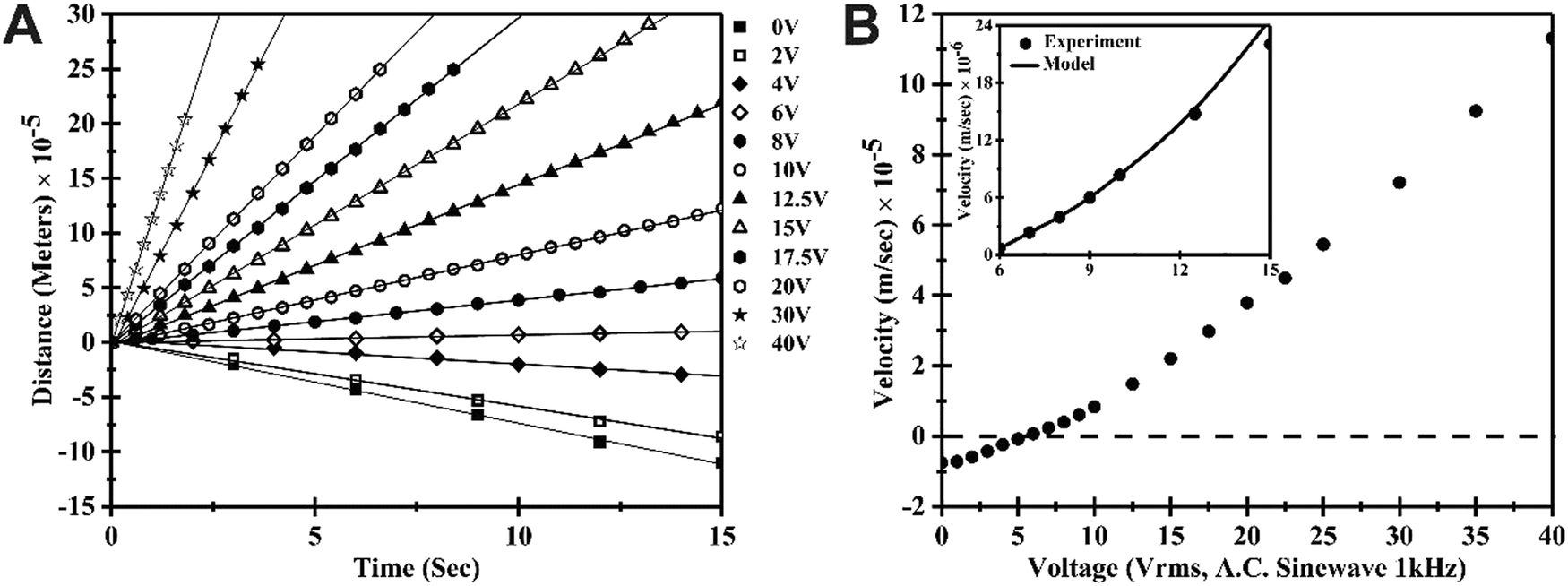 | ||
| Fig. 3 (A) The distance moved versus time by the tip of a finger-shaped electrically confined domain (dashed box in Fig. 1B(b)) in the x-direction for a range of applied different voltages. Linear fits to the data, shown by the solid lines, show that the tip moves at constant velocity. (B) The velocity versus voltage for the movement of the tip obtained from linear fits to the distance versus time data. The inset shows a theoretical fit to the data for low tip movement velocities. | ||
The data taken at all of the different voltages exhibit a linear dependence of the distance on the time, demonstrated by the solid straight line regression fits through each set of data points in Fig. 3A. A negative gradient is found for applied voltages below VC, with the data for V = 0 V showing the largest negative gradient and the highest negative velocity. As described in Section 3.1, the energy of elastic distortion around the domain wall and the energy cost of the defect line within the wall leads to a torque that acts to straighten the wall and retract the intercalated domains, pulling the tip in the negative direction when the electric field confinement is removed. The gradient increases monotonically as the voltage is increased, changing from negative to just positive when V = 6.0 V. This increase results from the torque on the nematic n-director due to electrical confinement becoming increasingly dominant at higher voltages over the torque that acts to straighten the domain wall, creating a more tortuous domain wall shape at higher voltages with a faster positive movement of the tip of the penetrating electrically confined domain.
Fig. 3B shows the velocity versus voltage dependence for the movement of the tip obtained from linear fits to the distance versus time data. The velocity increases monotonically in the voltage range from V = 0 V to V = 40 V, and exhibits a super linear dependence on voltage. The inset shows a theoretical fit to the data for low tip movement velocities, which will be discussed in Section 3.4. Hence the key observations are that the electric field constrained domain tip is held stationary at a critical stabilising voltage VC = 5.7 V, it moves with a constant velocity along a line in the negative x-direction under a lower applied voltage ΔV = V − VC < 0, and it moves with a constant velocity in the positive x-direction under a higher voltage when ΔV = V − VC > 0, where |ΔV| determines the velocity in the range −7.5 × 10⁻⁶ m s−1 to 113 × 10−6 m s−1. The tip can therefore be moved and positioned on demand, controlled by the magnitude of the applied voltage.
3.4 Theoretical description of the topological defect line dynamics
A nematic continuum theory-based dynamic model was developed which reproduces all of the key features of electrically confined domain evolution that have been observed in the experiments. We provide a summary here of the theory, further details are given in Supplementary file F2 (ESI†). The orientation of the nematic n-director was described by a tilt angle θ(x,y,z,t) relative to the y direction, and a nematic director of the form n = (0,cosθ,sinθ), as illustrated in Fig. 1. The HAN alignment states were then described by a linear variation of the tilt angle in the z-direction,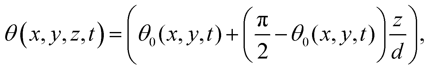 | (1) |
The Frank elastic energy Ef is given by,
 | (2) |
The periodic electric field produced by the interdigital electrodes is modelled by the function
 | (3) |
 | (4) |
Assuming that the electric field reorientation is stronger closest to the electrodes, we include a surface energy effect only at the lower surface, so that the surface energy is
 | (5) |
The rate of dissipation due to n-director rotation, parameterised by a phenomenological viscosity γ that is related to the nematic rotational viscosity, γ1, is
 | (6) |
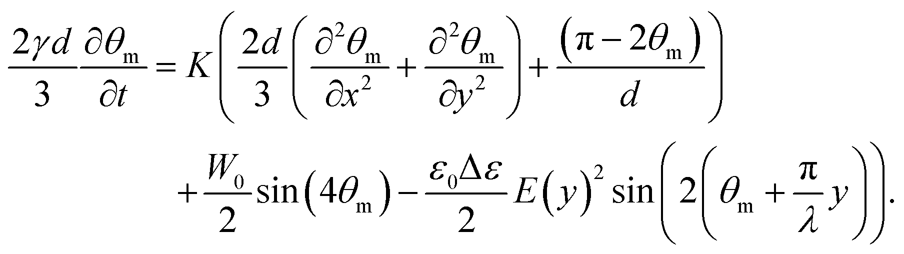 | (7) |
Dynamic simulations results produced by solving eqn (7) are shown in Fig. 4 (see also Supplementary movie M3, ESI†). Eqn (7) is non-linear in θm and there is a large spatial variation of θm across the nematic layer, particularly across the domain wall since the two equilibrium mid-layer orientations are separated by Δθme = π/2 rad. If we consider the behaviour at a single point, and perturb eqn (7) about one of the long-time equilibrium states, that would result in a solution that is exponential in time.40 However, here we are concerned with the nonlocal motion of the wall as a forced travelling wave. Due to the bistability, i.e. both HAN states being possible, the full non-local dynamic solution of eqn (7) is of a soliton-like travelling wave form.41 Time dependent solutions for θm(x,y,t) were produced with the aid of a commercial finite element partial differential equation solver39 using the following parameters: γ = 2.49 N s m−2; W0 = 55 × 10−5 J m−2; d = 13 × 10−6 m; K = 7.5 × 10⁻¹² N; Δε = 12.3; and λ = 160 × 10−6 m. The colours in Fig. 4 indicate the value of the tilt angle of the director in the middle of the cell, θm(x,y,t), as a function of position. The boundary lines of abrupt change in colour correspond to highly localised jumps in the values of the tilt angle on crossing the domain walls between the two possible opposing tilt domains. The boundary conditions were selected to produce a diagonal domain wall separating two opposing HAN states as the initial zero voltage equilibrium state in the simulation, shown in Fig. 4A. This emulated the experimental situation previously shown in the optical micrograph in Fig. 1A(b). Voltages were then applied in the simulation as in a similar sequence to that described at the beginning of Section 3.3, i.e. 9 V for 16.8 s, followed by changing the voltage to V = 5.5 V for 16.8 s. The value of the energy barrier W0 was adjusted to ensure that the value of the critical stabilising voltage in the model of 5.5 V was close to the value of VC found in the experiments. This procedure resulted in the static domain wall structure shown in Fig. 4B, which reproduces all the key features observed experimentally in the optical micrograph in Fig. 1B(b), including the kink across the region between electrodes, and the tips of the finger shaped domains where the domain wall crosses above the electrodes. The voltage in the simulation was increased back to 9 V which caused the tip regions to move again in the x-direction. This was accompanied by further domain wall deformation and encroachment of the electrically confined finger shaped domains into the regions initially occupied by the oppositely tilted HAN domain. Fig. 4C shows a snapshot of the domain wall during this dynamic extension process.
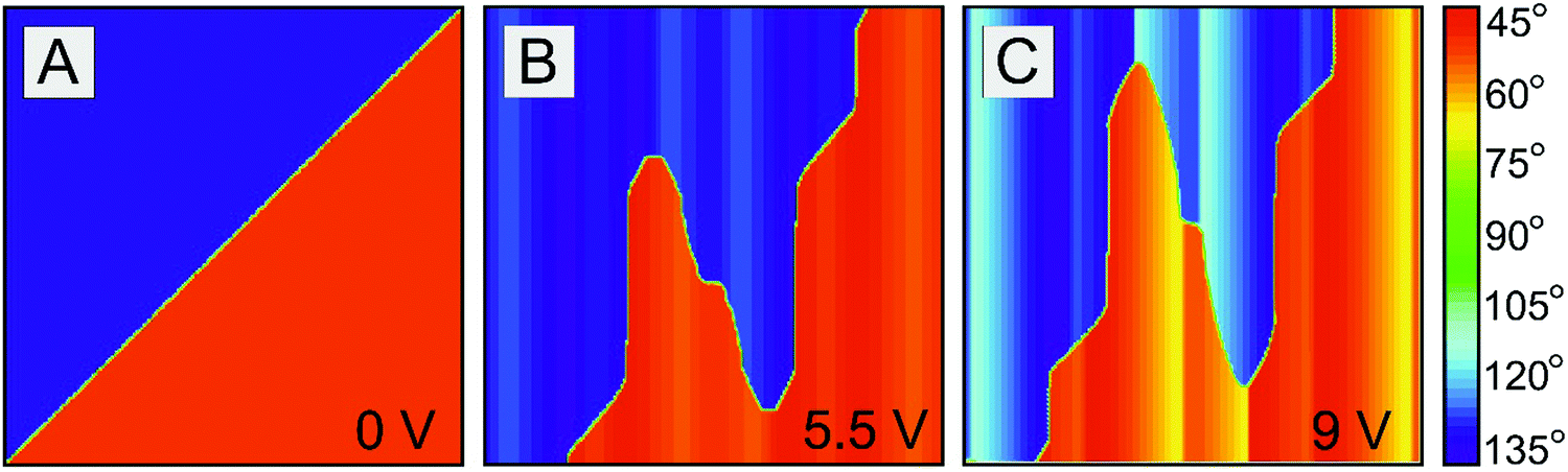 | ||
| Fig. 4 Numerical simulations of the time evolution of the domain wall (solid line) between two opposing HAN domains under the application of different voltages. The colours indicate the value of the tilt angle of the director in the middle of the cell, θm(x,y,t), according to the legend given to the right of the figure. (A) Zero volt equilibrium state. (B) The distorted static domain wall shape obtained after a period of dynamic deformation with 9 V applied, followed by abruptly changing the voltage to 5.5 V which arrested the dynamic domain evolution. This shows a close resemblance to the experimental optical texture in Fig. 1B(b). (C) A snapshot of the domain wall during dynamic extension after voltage had been again increased to 9 V. | ||
The inset velocity versus voltage graph in Fig. 3B demonstrates an excellent fit between the theoretical model and the experiment results at low voltages when V ≥ VC, using only the values of γ and W0 in eqn (7). as the adjustable fitting parameters. The quality of fit deteriorates at higher voltages, above 12 V, where the highly distorted regions localised around the defects embedded in the domain wall move closer to the substrates (see also Supplementary file F1, ESI†). This cannot be described in our model which neglects the z-direction. Hence the model reproduces a critical stabilising voltage, it also quantitatively describes the observed linear distance versus time behaviour and super-linear voltage dependence of the velocity for applied voltages immediately above this value, and also accurately reproduces the observed domain structures and domain wall shapes. This level of agreement provides confidence that we have captured the key physical nematic n-director structures and switching mechanisms produced via electrical confinement of the n-director, in our model and our interpretation of the experimental observations.
3.5 Electrically controlled topological micro cargo transportation
We now demonstrate how a colloidal micro particle can be collected and transported on demand via the voltage controlled motion of the domain wall. Polymer microspheres of density 1.05 g cm−3 and diameter 5.0 ± 0.1 μm were dispersed within the nematic carrier fluid. These had been treated with trichloro(octyl)silane to impart homeotropic alignment of E1 at the surface of the particle. Since the particles have homeotropic surface treatment, whilst the lower substrate of our device has planar nematic alignment, the uniform director field near the wall is incompatible with the director distortions around the sphere. The balance between the elastic repulsion from the wall and the gravity force driving sedimentation is expressed by eqn (6) of ref. 2, which gives the equilibrium height zelastic of an elastically levitating particle. The parameters for our system (K = 7.5 pN, R = 2.5 μm, Δρ = 40 kg m−3) predict that zelastic = 17 μm. Hence elastic forces are more than sufficient to prevent sedimentation in our device which has a layer thickness of d = 13 μm and so micro particles are located within the layer and away from surfaces (see also Supplementary file F1, ESI†).Fig. 5 shows a series of snapshots of the device under a polarising microscope that follow the dynamic process of a moving domain wall interacting with one of the particles, including collection, trapping, and transporting the particle. In Fig. 5A, a voltage of 7 V is applied to the device, which is above the critical stabilising voltage, VC = 5.7 V. This causes the domain wall to elongate, moving in the positive x-direction and also towards the nearest electrode edge in the negative y-direction where it connects with an initially separate micro particle. The micro particle is static under an applied voltage for 12 seconds, up until the point at which the wall and the particle connect, indicating an absence of significant thermally or electrically driven flow in the sample. The bright line that is visible in the optical micrograph to the top left of Fig. 5A corresponds to director reorientation close to the edge of the electrode under the action of a voltage. This reorientation is also reproduced in the results of the numerical simulations, Fig. 4C. The applied voltage is then abruptly reduced to 1 V at 14 s, below VC, which causes the domain wall to retract and move in the negative x direction. Fig. 5B shows how the particle has adhered to the domain wall and moves with the retracting wall, remaining at the high curvature tip as it moves in the negative x direction. Hence the micro sphere has been attracted to and trapped at the region of strong elastic deformation at the domain wall.42,43 A video demonstrating particle collection is given in Supplementary movie M4 (ESI†).
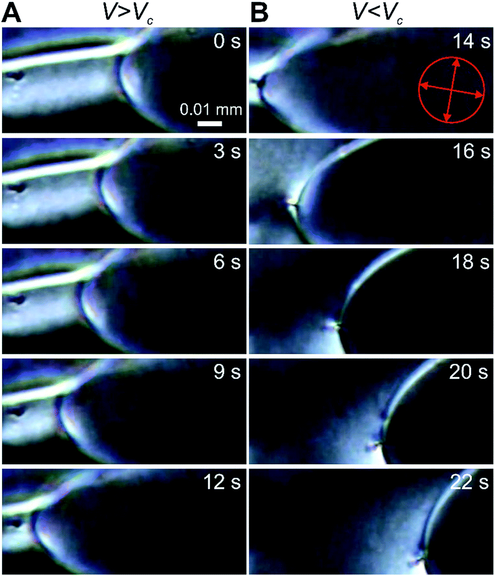 | ||
| Fig. 5 Optical micrograph of the nematic layer under plane-polarised light with a spherical micro particle towards the left hand side of the images. A domain wall is shown trapping and collecting the particle: (A) the wall dynamically extends and moves to the left under applied voltage 7 V, above VC (where VC = 5.7 V), overlapping the position of the particle. (B) At time 14 s the voltage is abruptly reduced to 1 V, below VC, and the domain wall retracts whilst transporting the adhered particle at its tip. The crossed polariser and analyser orientations are shown by the arrows in the circle on the micrograph. | ||
Fig. 6 shows a series of snapshots of the device under a polarising microscope that follow the dynamic process of a moving domain wall transporting and positioning a micro particle. In Fig. 6A the particle was moving in the negative x direction when the applied voltage is 6.5 V, above the critical stabilising voltage VC, in Fig. 6B the particle stopped when the applied voltage was set exactly to VC = 5.7, and in Fig. 6C the particle was moving in the positive x direction when the applied voltage was decreased to 4 V. In each case the images show that the particle remained located to the region of the high curvature tip of a finger-shaped electrically confined domain. A video demonstrating this controlled micro particle movement is given in Supplementary movie M5 (ESI†).
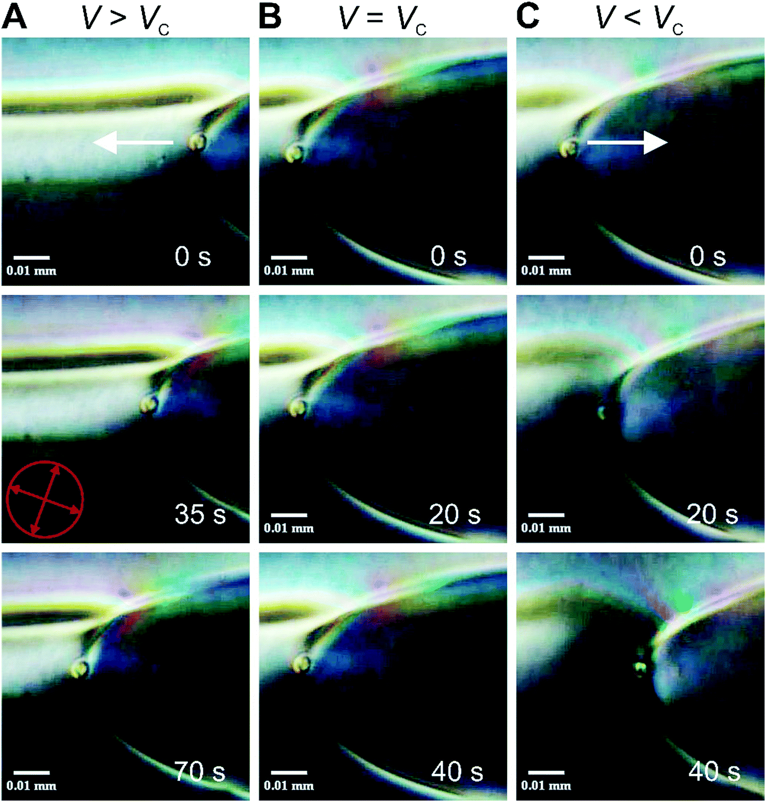 | ||
| Fig. 6 Optical micrographs showing transportation of a colloidal micro particle by the high curvature tip of the electrically confined finger shaped domain: (A) the particle was moved in the negative x-direction when the applied voltage was 6.5 V, above the critical stabilising voltage (V > VC). (B) The particle is held stationary when V = VC = 5.7 V. (C) The particle is moved in the positive x-direction when the applied voltage was 4 V, below the critical stabilising voltage (V < VC). The crossed polariser and analyser orientations are shown by the arrows in the circle on the micrograph. | ||
Hence, voltage control of the distortion and extent of the domain wall using the magnitude of voltage relative to the critical stabilising voltage, ΔV = V − VC provides both positive and negative precision bidirectional movement of the micro particle along a line. At any point, setting the voltage abruptly to VC stops the particle movement and holds the particle at the position that it has reached, providing the capability to reversibly place the trapped micro particle on demand.
4 Conclusion
We have created and demonstrated the time dependent electric field reconfiguration and manipulation of a wall containing a topological line defect between two opposing hybrid aligned nematic liquid crystal domains. A high curvature tip region of the wall can be moved with constant velocity on demand in both positive or negative directions, or held stationary at any position during its travel, simply by tuning the value of a low applied voltage. We have elucidated the important physical processes acting within the layer within a theoretical model that accurately reproduced the observed time and voltage dependent shapes of the meandering domain wall.In the model the anchoring strength parameter, W0, expresses the amount of energy required to break surface anchoring and transform from one hybrid aligned state to the opposing state. Increasing the value of W0 in the model increased the value of the critical stabilising voltage VC. Hence the value of the parameter VC in our system can provide insight into the anchoring strengths at the surface. Future work will investigate how VC depends systematically on the surface anchoring since the strength of both planar and homeotropic anchoring, including on the particle, can be tuned.24,44,45 In previous work a particle with homeotropic alignment has been shown to be readily attracted to and trapped by the defect, whilst if the surface alignment on the particle is planar the situation is more complex. A repulsive interaction and energetic barrier can exist between the planar particle and disclination lines of strength +1 or ½ and so an applied force is required to trap the particle.46
We have exploited these domain manipulation capabilities in a technological micro cargo transport application, providing electrically controlled linear translation and precision positioning of a colloidal particle in a soft matter device. Our system avoids the requirement for externally imposed and controlled flow, and also avoids the requirement for alignment patterning or lateral confinement walls and structures within the liquid layer. Our technique offers the opportunity to transport either neutral or charged particles, whilst the use of an A.C. voltage avoids electrochemical degradation effects that can be associated with D.C. electric fields. The research has potential relevance to the design of the next generation of micromachines and lab-on-chip devices, providing the possibility of using voltage actuated defect wiring or collection and movement of individual particles to regions where self-assembly occurs.47–50 This opens up avenues for the voltage assisted assembly of functional materials for soft matter electronically controlled sensing and optoelectronic devices.
Conflicts of interest
There are no conflicts to declare.Acknowledgements
ASB and AS gratefully acknowledge Nottingham Trent University (Nottingham UK) and Merck Chemicals Ltd (Chilworth UK) for PhD Scholarship funding. We gratefully acknowledge Dr H. Arasi, Dr O. Parri and Dr R. P. Tuffin from Merck Chemicals Ltd for the provision of materials and advice, Dr D. Koutsogeorgis for his help with producing the thermally evaporated planar alignment layers, and Dr A. M. J. Edwards for his help with image analysis.References
- G. M. Whitesides and B. Grzybowski, Science, 2002, 295, 2418–2421 CrossRef CAS PubMed.
- O. D. Lavrentovich, Soft Matter, 2014, 10, 1264–1283 RSC.
- I. Muševič, Liquid Crystal Colloids, Springer International Publishing, Springer Nature Switzerland AG, 2017 Search PubMed.
- Ivan I. Smalyukh, Annu. Rev. Condens. Matter Phys., 2018, 9, 207–226 CrossRef.
- O. D. Lavrentovich, I. Lazo and O. P. Pishnyak, Nature, 2010, 467, 947–950 CrossRef CAS PubMed.
- Y. Sasaki, Y. Takikawa, V. S. R. Jampani, H. Hoshikawa, T. Seto, C. Bahr, S. Herminghaus, Y. Hidaka and H. Orihara, Soft Matter, 2014, 10, 8813–8820 RSC.
- T. Ohzono and J. I. Fukuda, Nat. Commun., 2012, 3, 701–707 CrossRef PubMed.
- A. Sengupta, C. Bahr and S. Herminghaus, Soft Matter, 2013, 9, 7251–7260 RSC.
- H. Yoshida, K. Asakura, J. Fukuda and M. Ozaki, Nat. Commun., 2015, 6, 7180–7807 CrossRef CAS PubMed.
- C. Peng, T. Turiv, Y. Guo, S. V. Shiyanovskii, Q.-H. Wei and O. D. Lavrentovich, Sci. Adv., 2016, 2, e1600932 CrossRef PubMed.
- Y. Luo, D. A. Beller, G. Boniello, F. Serra and K. J. Stebe, Nat. Commun., 2018, 9, 3841–3851 CrossRef PubMed.
- N. D. Mermin, Rev. Mod. Phys., 1979, 51, 591–648 CrossRef CAS.
- M. V. Kurik and O. D. Lavrentovich, Phys.-Usp., 1988, 31, 196–224 CrossRef.
- G. P. Alexander, B. G. G. Chen, E. A. Matsumoto and R. D. Kamien, Rev. Mod. Phys., 2012, 84, 497–514 CrossRef CAS.
- S. Chandrasekhar, Liquid Crystals, Cambridge University Press, Cambridge, 1992 Search PubMed.
- P. G. De Gennes and J. Prost, The physics of liquid crystals, Clarendon Press, Oxford, 1993 Search PubMed.
- A. Sengupta, S. Herminghaus and C. Bahr, Liq. Cryst. Rev., 2014, 2(2), 73–110 CrossRef CAS.
- H. Agha and C. Bahr, Soft Matter, 2016, 12(18), 4266–4273 RSC.
- H. Agha and C. Bahr, Soft Matter, 2018, 14(4), 653–664 RSC.
- A. Sengupta, B. Schulz, E. Ouskova and C. Bahr, Microfluid. Nanofluid., 2012, 13(6), 941–955 CrossRef CAS.
- H. P. Kim, J. Park, J. Han, J. Han and D. Seo, IEEE Electron Device Lett., 2013, 34(2), 283–285 Search PubMed.
- H. Yokoyama and H. A. V. Sprang, J. Appl. Phys., 1985, 57, 4520–4526 CrossRef CAS.
- P. Kumar, S. Y. Oh, V. K. Baliyan, S. Kundu, S. H. Lee and S. W. Kang, Opt. Express, 2018, 26(7), 8385–8396 CrossRef CAS PubMed.
- Y. Cui, R. S. Zola, Y.-C. Yang and D.-K. Yang, J. Appl. Phys., 2012, 111(6), 063520 CrossRef.
- D. Dunmur and W. Miller, J. Phys., Colloq., 1979, 40(C3), 141–146 CrossRef.
- D. A. Dunmur and G. R. Luckhurst, Physical properties of liquid crystals: nematics, Institution of Engineering and Technology, London, 2007 Search PubMed.
- G. W. Gray, K. J. Harrison and J. A. Nash, Electron. Lett., 1973, 9, 130–131 CrossRef CAS.
- P. J. Collings and M. Hird, Introduction to Liquid Crystals: Chemistry and Physics, CRC Press, USA, 1997 Search PubMed.
- M. J. Bradshaw and E. P. Raynes, Mol. Cryst. Liq. Cryst., 1981, 72(2–3), 35–42 CrossRef CAS.
- V. Fréedericksz and V. Zolina, Trans. Faraday Soc., 1933, 29(140), 919–930 RSC.
- E. Meijering, O. Dzyubachyk and I. Smal, in Methods in Enzymology, ed. P. M. Conn, Academic Press, 2012, vol. 504, pp. 183–200 Search PubMed.
- C. A. Schneider, W. S. Rasband and K. W. Eliceiri, Nat. Methods, 2012, 9, 671–675 CrossRef CAS PubMed.
- C. Tsakonas, A. J. Davidson, C. V. Brown and N. J. Mottram, Appl. Phys. Lett., 2007, 90, 111913 CrossRef.
- C. L. Trabi, C. V. Brown, A. A. T. Smith and N. J. Mottram, Appl. Phys. Lett., 2008, 92, 223509 CrossRef.
- K. H. Yang, J. Appl. Phys., 1990, 67, 36–39 CrossRef CAS.
- S. Takahashi, J. Appl. Phys., 1991, 70, 5346–5350 CrossRef CAS.
- H. Y. Chen, K. X. Yang and Z. Y. Lin, J. Phys. D: Appl. Phys., 2010, 43(31), 315103 CrossRef.
- N. Éber, P. Salamon and Á. Buka, Liq. Cryst. Rev., 2016, 4(2), 101–134 CrossRef.
- COMSOL Multiphysics® v. 5.4, http://www.comsol.com, COMSOL AB, Stockholm, Sweden.
- I. W. Stewart, The Static and Dynamic Continuum Theory of Liquid Crystals A Mathematical Introduction, Taylor and Francis, London, New York, 2004 Search PubMed.
- N. V. Madhusudana, J. F. Palierne, Ph. Martinot-Lagarde and G. Durand, in Solitons in Liquid Crystals, ed. L. Lam and J. Prost, Springer-Verlag, New York, 1991, ch. 8 Search PubMed.
- P. Poulin, H. Stark, T. C. Lubensky and D. A. Weitz, Science, 1997, 275, 1770–1773 CrossRef CAS PubMed.
- D. Voloschenko, O. P. Pishnyak, S. V. Shiyanovskii and O. D. Lavrentovich, Phys. Rev. E: Stat., Nonlinear, Soft Matter Phys., 2002, 65, 060701 CrossRef CAS PubMed.
- S. A. Jones, J. Bailey, D. R. E. Walker, G. P. Bryan-Brown and J. C. Jones, Langmuir, 2018, 34, 10865–10873 CrossRef CAS PubMed.
- Z. Eskandari, N. M. Silvestre, M. M. Telo da Gamaa and M. R. Ejtehadi, Soft Matter, 2014, 10, 9681–9687 RSC.
- I. I. Smalyukh, B. I. Senyuk, S. V. Shiyanovskii, O. D. Lavrentovich, A. N. Kuzmin, A. V. Kachynski and P. N. Prasad, Mol. Cryst. Liq. Cryst., 2006, 450, 279–295 Search PubMed.
- T. Yamamoto and M. Yoshida, Langmuir, 2012, 28, 8463–8469 CrossRef CAS PubMed.
- I. Muševič, M. Škarabot, U. Tkalec, M. Ravnik and S. Žumer, Science, 2006, 313, 954 CrossRef PubMed.
- I. Muševič, M. Škarabot, S. Žumer and M. Ravnik, EP1975656, Priority date 1 Oct., 2018.
- J. B. Fleury, D. Pires and Y. Galerne, Phys. Rev. Lett., 2009, 103, 267801 CrossRef PubMed.
Footnote |
| † Electronic supplementary information (ESI) available: File F1 provides additional experimental details; file F2 describes the development of the theoretical model; movie M1 shows electrohydrodynamic convection in response to a low frequency A.C. sinewave driving voltage (but no convection at 1 kHz); movie M2 shows the tip of a finger shaped domain wall moving at different speeds at different applied voltages; movie M3 shows theoretical dynamic domain wall evolution; movie M4 shows micro cargo collection; movie M5 shows micro cargo transport. See DOI: 10.1039/c9sm01956a |
| This journal is © The Royal Society of Chemistry 2020 |