
 Open Access Article
 This Open Access Article is licensed under a Creative Commons Attribution-Non Commercial 3.0 Unported Licence
15% enhancement of the photocurrent at the maximum power point of a thin film solar cell†
Himanshu
Shekhar
and
Nir
Tessler
 *
*
Microelectronics and Nanoelectronics Centers, Electrical Engineering Department, Technion Israel Institute of Technology, Haifa 32000, Israel. E-mail: nir@technion.ac.il
First published on 18th September 2020
Abstract
Recent efficiency enhancement of organic solar cells has been achieved through material and chemical engineering of the chemistry and morphology of the donor–acceptor junction. Inducing band bending at the junction through ground state charge transfer between the donor and acceptor is an important route but realising it through chemical design is challenging. Here we demonstrate a device engineering approach to modify the junction's electronic structure improving the maximum power point (MPP) current by 50% and the current at 80% of the open-circuit voltage (0.8 VOC) by 30%. We report modulation-doping of the hole transport layer while exploring the effect of the thin doped-layer distance from the junction. To avoid ambiguity in the interpretation of the results, we utilize a bi-layer structure and choose to insert the dopant into a wide band gap donor so as to avoid direct interaction with photogenerated excitons. Using a device model, we show that the doped-layer induces long range enhancement of the internal electric field, all the way between the p-type doped-layer and the cathode. Such enhancement is especially important at the MPP where the contact-induced internal electric field tends to diminish. In state of the art solar cells, the current at the MPP is at least 15% below the short-circuit current (JSC) suggesting that our method might induce improvement in such cells too (18% × 1.15 = 20.7%).
Introduction
The power conversion efficiency (PCE) of organic solar cells is greatly influenced by the rate at which coulombically bound photogenerated charge pairs dissociate into free carriers at the cell's donor–acceptor junction. In solar cells, the built-in electric field at the maximum power point (i.e., close to the open-circuit voltage (VOC) or flat-band condition) is close to zero, suggesting strong competition between dissociation and separation of charges with recombination losses.1,2 This is, at least partially, why high VOC cells tend to have relatively low fill factors3,4 while theoretically it is supposed to go up with VOC.5Most of the effort to mitigate this effect has been in the material domain and among the various strategies employed one can find that controlling the morphology, minimizing the binding energy, or inducing ground state energy transfer achieves favourable band bending at the junction.6–10 It has also been suggested that the inevitable presence of disorder contributes favourably to charge generation.11–13
Understanding the physics of the efficiency of rate of transition from the bound charge transfer (CT) state to free carrier is of immense importance and has been a topic of intensive investigation.14–16 We note that this list nowhere represents the amount of work that has been done in the last 10 years and much can be found in recent reviews.17 In the context of the current paper, we should mention that several reports have shown the importance of the strength of the device electric field on the photogeneration in organic solar cells.4,14,15,18–20
Efficiency improvement has been largely due to efforts in material chemistry where single Junction efficiency has reached 18%.21,22 However, predictions of the maximum efficiency limit place it slightly above 20%.23,24 In this context, device design strategies may help and bridge the gap. We note that there exist several studies in this direction where different device structures have been suggested to improve the efficiency of organic based solar cells by shifting the contact workfunction25,26 or introducing dopants.27 Initially, doping was used mainly to enhance the contact properties and later also as a charge recombination layer in multi-junction cells.27 Doping is also used in inorganic cells and one can find examples showing insertion of δ-doping in the transport layer28–30 or a thin doped layer in the wetting layer (spacer) between quantum dots in the active region.31,32 Here too, doping the transport layer resulted in enhancing either its conductivity28 or charge selectivity.30 Back to the organic cells, recently, dopants have been introduced also into the bulk of the active region33–35 where it was suggested that the dopants may assist in morphology control, trap filling, or maybe screening of the coulomb-binding energy of the CT states. Since this paper extensively uses the concept of doping we find it important to specify what the terms δ-doping and modulation doping mean, in this paper at least. We follow the definitions most common regarding inorganic semiconductor devices. δ-doping is typically used in cases where the doping is confined to a few atomic layers (1–3 mostly). It is called δ since on both sides of the “zero” width region the semiconductor is undoped. In cases where the doped region is wider the use of δ is not appropriate anymore and one refers mainly to the fact that now the layer is not uniformly doped. So a 10 nm doped layer within a 40 nm undoped semiconductor constitutes modulation doping.
Here we explore the potential of using doping to induce an electric field at the junction thus enhancing the charge separation efficiency. In previous work, we have presented a device design26 for overcoming the electrode pinning within the gap36 so as to enhance the built-in potential and through it also the open-circuit voltage. In this paper, we report the effect of modulation-doping, with the p-dopant C60F48 in this case, on the exciton dissociation and separation efficiency at the organic heterojunction. To avoid ambiguity in the interpretation of the physical picture we employ a planar heterojunction (PHJ) structure37–39 and use two well studied materials, C70 and 1,1-bis [(di-4-tolylamino) phenyl] cyclohexane (TAPC).40–43 In our case, another advantage of using a planar heterojunction is that it has been shown that the open circuit voltage of such cells is not limited by the electrode contact-barriers.39 We experimentally show that doping directly at the junction has a negative effect but distancing the dopants away from the junction has a positive impact on device performance.
Measuring the low intensity external quantum efficiency (EQE) as well as the intensity dependent quantum efficiency (QE) across 5 orders of magnitude reveals that both the generation and recombination processes are affected by the new device structure. Theoretical investigation of the effect of the dopant's Coulomb potential on the junction's energetic landscape reveals the presence of an enhanced local electric field. Our results show that the doping induced potential gradient enhances exciton dissociation, reduces charge recombination, and consequently has a profound effect on the overall efficiency of the device.
Experimental results
Device structure and modulation-doping
In this article, we show the effect of doping a thin layer in the vicinity of the donor–acceptor junction on exciton dissociation and charge separation in an organic heterojunction device. We probe the cumulative strength of exciton dissociation and charge separation in differently doped devices by directly measuring their photogenerated current. We conducted this study on TAPC and C70 based small molecule planar heterojunction solar cells and used the p-dopant C60F48 to dope a small section of TAPC (i.e. modulation-doping) next to the junction. The schematic of the device structure is shown in Fig. 1a and the energy level diagram of the materials used is presented in Fig. 1b (see also Fig. S1 in the ESI†). For this study, we have chosen a planar heterojunction structure over bulk heterojunction structures since bi-layer devices allow decoupling of the generation-recombination at the junction from the transport across the device.42 As per the initial discovery that fluorinated fullerenes (C60Fxx) can dope organic semiconductors,44 fluorinated fullerenes have the advantage of efficient doping45 as well as stability.42,46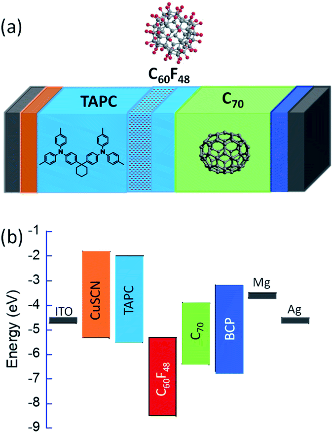 | ||
| Fig. 1 (a) Schematic description of the device structure consisting of ITO/CuSCN/TAPC/C60F48-doped TAPC/TAPC/C70/BCP/Mg/Ag. The chemical structures of the active materials are embedded in the device structure. (b) Energy level diagram of the materials used in this study. | ||
To verify that the structure in Fig. 1a can be realised we had to ensure that the concept of modulation-doping can be realised in relatively soft organic materials which are prone to molecular interdiffusion. To this end we constructed a similar structure having the following nominal layer thicknesses (from top to bottom): C70 (50 nm)/TAPC (10 nm)/TAPC:C60F48 (10 nm)/TAPC (50 nm)/CuSCN (70 nm)/ITO. Due to technical constraints, the measurement was performed slightly more than a week following the layer fabrication. This structure was transferred to a Time-of-Flight Secondary Ion Mass Spectrometry (ToF-SIMS) chamber and the relevant elemental analysis results are shown in Fig. 2a. We rely on the following to distinguish between the materials that are close to the heterojunction. C70 has only carbons, only TAPC contains nitrogen, and only C60F48 contains fluorine. We note that the C60F48 is fully within the TAPC layer and that its spatial extension is similar to the nominal value (10 nm). We repeated the measurement about a week later using a slower etch rate (Fig. S2, ESI†) and the only difference was a slight improvement in the resolution. We also constructed a complete device and its cross-sectional scanning tunnelling microscope image is shown in Fig. 2b. We note that the CuSCN layer has a slightly uneven surface and that the active layer conforms to it. The actual thickness of the layer is close to the nominal value but for the CuSCN being rough and uneven. Also, the thickness of the C70 layer is similar to the one deduced from the SIMS data.
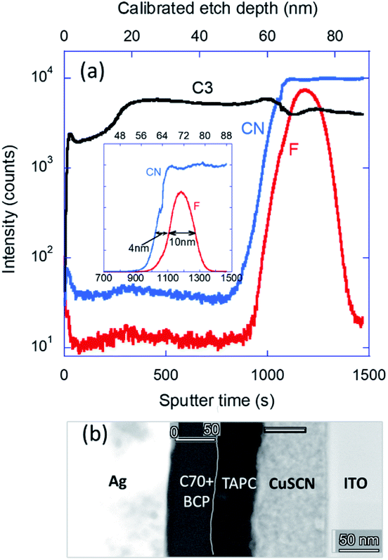 | ||
| Fig. 2 (a) ToF-SIMS analysis of the bi-layer having nominal layer thicknesses of C70 (50 nm)/TAPC (10 nm)/TAPC:C60F48 (10 nm)/TAPC (50 nm)/CuSCN (70 nm)/ITO. The estimated position error is ±2 nm. (b) High resolution scanning tunnelling microscope image of a complete device cross section. | ||
Undoped versus modulation-doped device
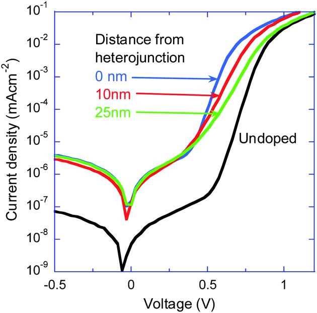 | ||
| Fig. 3 Current density versus applied bias of a reference undoped-device and devices with varying separation between the doped-layer and the hetero-junction (as marked on the figure). The measurements were carried out in the dark. | ||
Upon adding the doped-layer the reverse leakage current at −0.5 V increases from 70 pA cm−2 to ∼3.5 nA cm−2 indicating enhanced conductivity of the device. We also note that the diode ideality factor (n, exponential rise) changes and assumes the values of n = 1.1 (undoped), n = 1.4 (0 nm), n = 1.8 (10 nm), and n = 2 (25 nm). First, these differences show that positioning of the doped-layer is accurate and stable enough to allow for this fine spatial resolution, in agreement with Fig. 2. Second, the standard TAPC:C70 diode (reference diode here) was extensively analysed in ref. 42 and despite n ∼1 the recombination was found to be composed of both Langevin-like bimolecular and trap-assisted recombination. The trend of the doped devices suggests that the monomolecular recombination becomes more dominant. However, the presence of the modulation-doping makes these devices non-standard ones and hence such a standard interpretation of the J–V, including the ideality factor, should be taken with a pinch of salt. We will defer further analysis of the dark-J–V to the simulation section.
Having established that the position of the modulation-doping affects the device characteristics, we move to examine its effect on the photocurrent conversion efficiency (PCE). Fig. 4a shows the J–V curves of the same devices as in Fig. 3 but measured under one sun illumination. Doping just at the junction (0 nm) degrades the device performance by primarily shifting the VOC from 0.95 V to 0.77 V. Distancing the doped-layer by 10 nm recovers the VOC and significantly improves both the fill factor and the short-circuit current (JSC). The JSC of the device with the doped layer 10 nm away is 46% higher compared to that of the undoped device. Moving the doped-layer even farther reduces the efficiency only slightly as the J–V curve changes slightly towards the undoped case.
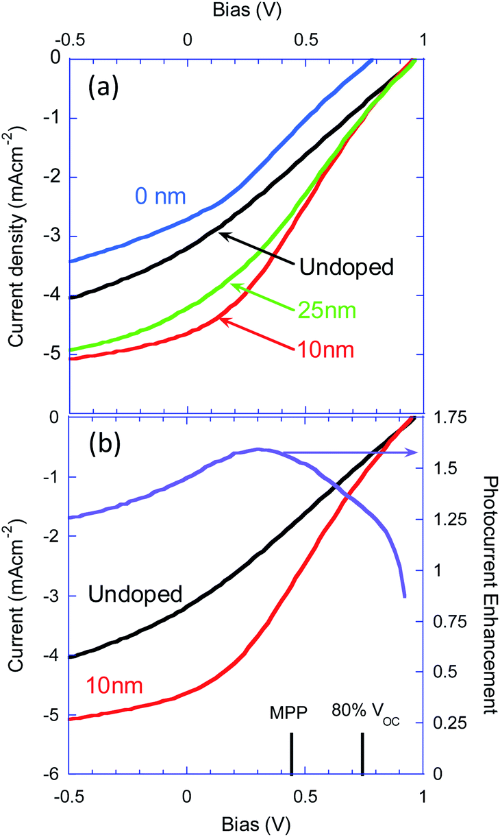 | ||
| Fig. 4 (a) Current density versus applied bias of a reference undoped-device and devices with varying separation between the doped-layer and the hetero-junction (as marked in the figure). The measurements were carried out under one sun illumination. (b) The J–V curves of (a) replotted (left axis) along with the current enhancement ratio (right axis). | ||
To quantify the improvement of the extracted current by placing the doped-layer 10 nm away from the junction we redraw in Fig. 4b the J–V curves for the undoped diode and diode with the doped layer 10 nm away and overlay on it the ratio between the two. Due to the poor performance of these devices the maximum power point (MPP) is slightly below 0.5 V (see Fig. 4b) and at this bias the current enhancement is 55%. In a better-behaved cell, the MPP would be closer to VOC. At V = 0.8 VOC the enhancement is 32% and at V = 0.9 VOC it is 15%. Namely, while the high enhancement of 55% could be associated with the device not being efficient to begin with, we can state that in a well-behaved cell the improvement at the MPP would be at least 15%. This statement is later backed by the simulation section that proves the generality of the source for this improvement. Also, Fig. S3 and S4† also include the dark and light J–V curves of the 3 nm and 6 nm spacing of the doped-layer from the junction. These figures suggest that only for a nominal spacing of 10 nm is the doped-layer fully decoupled from the junction.
As 15% enhancement is still a rather high number, we try to find its origin by examining additional characteristics measured at short circuit (JSC enhancement was 46%). Fig. 5 shows the spectrally resolved external quantum efficiency measured for the 4 devices used for the previous results (Fig. 4). The inset in Fig. 5 shows the same data but on a logarithmic scale which emphasises the sub-gap states. The excitation intensity was kept well below 1 mW cm−2 so as to be in the intensity independent regime presented in Fig. 6 (the plateau part of the curve). The relative values in the 400–700 nm range are in line with the trend found for the JSC currents. The sub-gap EQE shows indeed that doping away from the junction has no effect on the sub-gap states at the junction. Doping at the junction, however, seems to slightly reduce the optical activity of the sub gap states. This could be related to nanoscale morphology or state-filling (bleaching) but deciphering it is beyond the scope of this paper.
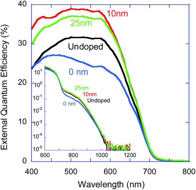 | ||
| Fig. 5 Measured external quantum efficiency as a function of excitation wavelength and using low light intensity for the four device structures (as marked in the figure). The inset shows the same data on the logarithmic scale emphasizing the sub-gap absorption. | ||
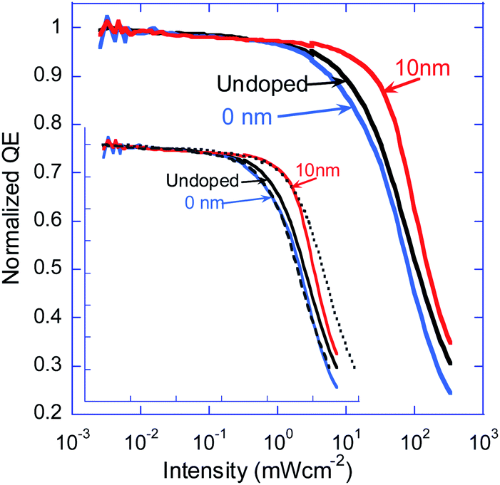 | ||
| Fig. 6 External quantum efficiency as a function of excitation intensity measured for the three device structures marked in the figure. The curves were normalised to their low intensity part. The excitation source was a white LED. The inset shows the same data plus the curve of the undoped device shifted to low intensity (dashed line) and to high intensity (dotted line). | ||
The VIS part of the EQE spectrum (Fig. 5) has two features that require further study. First, the EQE of the device with the doped layer 10 nm away is only about 25% higher compared to that of the undoped device, where the JSC showed 46% enhancement. Second, the spectral shape of the device with the doped layer 10 nm away is different from that of the undoped one. A potential reason for the difference between the 25% of the EQE and the 46% of the JSC could be the vastly different excitation densities used in the two cases (>2–3 order of magnitude difference). To address this issue, we utilize the method developed by Rappaport et al.47,48 for pristine materials which was later proved useful in also deciphering the losses in heterojunction ones.49–51 In short,47 at very low light intensity the device's quantum efficiency is intensity independent and in most cases represents the free charge generation efficiency (ref. 49 shows a case where this might not be accurate). The plateau in the EQE versus intensity curve is then followed by a decline in efficiency as higher order losses kick in. The position of the “knee” that marks the initial decay in EQE is a function of the interplay between the charge recombination and the charge extraction. If you know one you can use this curve to deduce the other or in cases where the two are interlinked, one can directly deduce both.47
Examining Fig. 6 we see that the higher order (>1) losses kick in at different intensities for the undoped and junction doped (0 nm) devices and the devices with the doped layer 10 nm away. Namely, compared to the reference device, the recombination for the junction-doped device and the device with the doped layer 10 nm away is more and less effective, respectively. Since for the device with the doped layer 10 nm away the dopants are clear of the junction, there is no reason to suggest that the recombination is affected and it is most likely that the extraction from the junction area becomes more efficient. Another attribute of the method developed by Rappaport et al. is that if the physical mechanisms do not change and only their relative magnitudes change, then shifting the curves horizontally should result in perfect overlap (Fig. 6 in ref. 48). The inset in Fig. 6 shows the same data as the main figure plus the curve for the reference (undoped) device shifted to lower (dashed) and higher (dotted) intensities. In the case of the junction-doped (0 nm) device we obtain a perfect overlap indicating that the only thing that happened is that the recombination became more significant. For the device with the doped layer 10 nm away it is impossible to obtain overlap across a wide range and hence we can state that the physical processes have changed. To address this point, we turn to optical and electrical modeling.
Optical and electrical modelling
The measured real and imaginary parts of the refractive index are shown in Fig. 7a and Fig. 7b, respectively. The indices of the doped and undoped TAPC are very similar but for a tiny hump at about 700 nm associated with the doping induced polaron absorption.53 The inset in Fig. 7b shows the absorbance of TAPC at different levels of molar ratio% (MR%) doping confirming the presence of doping induced absorption (film thickness ∼70 nm).
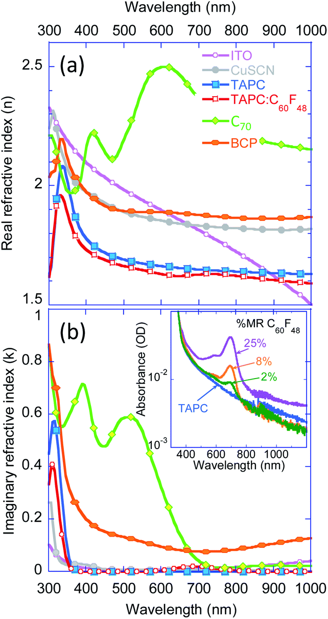 | ||
| Fig. 7 Real (a) and imaginary (b) refractive index of the materials used in the PHJ devices. The inset in (b) is the absorbance spectrum of ∼70 nm thick undoped TAPC and 25%, 8%, and 2% molar ratio C60F48 in TAPC. | ||
Fig. 8a shows the calculated wavelength-integrated electric field intensity distribution within the devices as a function of distance for the CuSCN/TAPC interface. The intensity was integrated across 450 nm to 700 nm and the vertical dashed line denotes the TAPC/C70 interface. A similar calculation where the spectrum is weighted by the sun spectrum as well as for 550 nm only, can be found in Fig. S5 in the ESI.† As the figure shows, since the doping hardly affected the refractive indices, there is no difference, in the field distribution, between the different device structures. Fig. 8b shows the power absorbed in the device in the first 15 nm of C70 from the junction. We chose 15 nm as it is a reasonable value for the exciton collection by the junction. The resulting spectral shape is very similar to that of the measured reference (undoped) device. Namely, thus far, the optical modeling did not provide any explanation for the differences found between the devices.
 | ||
| Fig. 8 (a) Calculated electric field intensity within the device active layers as a function of distance from the CuSCN/TAPC interface. The curve is an integration over the wavelength range 450–700 nm. (b) Calculated % of the power that is absorbed in the first 15 nm of C70 (70–85 nm in a). The calculations were done for the various device structures yielding indistinguishable results. | ||
Device simulations
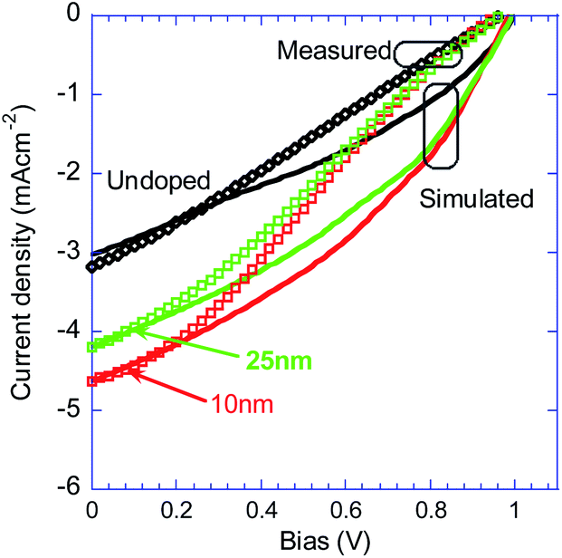
The device simulation details can be found in the experimental section under simulation settings. Measured and simulated dark current densities are shown in Fig. 9. As described in the Experimental section, the parameters for the different device structures were kept constant but for the 10 nm thick doped (5 × 10¹⁷ p-type) layer that was positioned either 10 nm or 25 nm away from the junction. Using the absorption of the charge-transfer (CT at ∼700 nm) to estimate the doping efficiency of C60F48 as a function of the host ionization energy54 suggests that the doping may be as high as 1019 cm−3. Interestingly, it was shown that the fraction of CT that dissociates into free charges could be as low as 10% of the values extracted through absorption.55 Simulating a range of doping levels, we found that the quality of the fit did not improve above 5 × 1017 cm−3 (see Fig. S7 in the ESI†). The agreement between the experimental and simulated results (Fig. 9) is very good suggesting that the main difference between the devices is captured by a drift-diffusion-Poisson based model.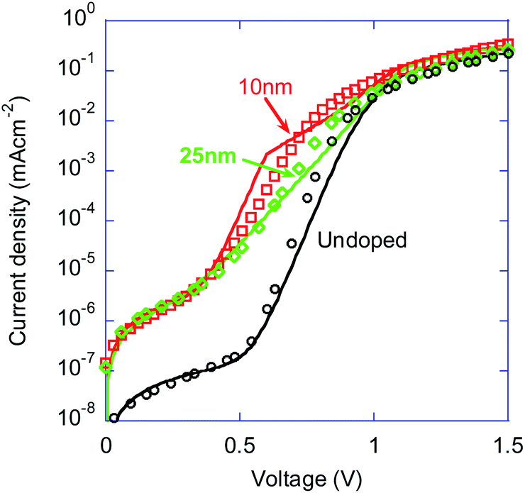 | ||
| Fig. 9 Measured (symbols) and simulated (lines) current densities as a function of bias and under dark conditions. For the doped devices we assumed a 10 nm thick TAPC doped (5 × 1017 cm−3) layer positioned 10 nm (red) or 25 nm (green) away from the junction. We manually added parallel (leakage) resistance of 3 × 10⁶ Ω and 105 Ω for the undoped and doped devices, respectively. | ||
To confirm that the difference between the three device structures is at the device level, we had to also simulate the J–V under sun illumination. Simulating using Sentaurus, we cannot implement the process of CT excitons splitting at the junction as well as the exciton binding energy that may be hindering it. To mimic these effects and come close to the real physics, we chose the following scenario:
1. Generation is of free electrons and holes and only in the first 10 nm of C70. Namely, holes are close enough to the TAPC interface so that they can diffuse to it.
2. To mimic the effect that the charges should not be generated as being free to move we introduce high bimolecular and monomolecular recombination into these 10 nm. This way, if charges are not swept-out efficiently they would recombine.
As before, the generation and recombination parameters were chosen such that the simulation of the undoped (reference) device will be as close as possible to the measured J–V. Next, a 10 nm doped layer was inserted, and the simulation was repeated. We note that the J–V enhancement for the device with the doped layer 10 nm away from the junction and the slight decline for the device with the doped layer 25 nm away, are in excellent agreement with the trend found in the measured data. Namely, the performance enhancement is indeed mostly at the device level and variations in material and basic processes are, at best, secondary.
Having deduced that the enhancement is at the device level one can visit the entire set of internal data produced by the simulations and identify the source. Fig. 11a shows the effect that led to the efficiency enhancement. As shown, the energy level diagram at short-circuit, for the reference (undoped) device, has a standard shape with the levels being linearly tilted to indicate the internal electric field associated with the energy difference between the two contacts (Vbi). For the device with the doped layer 10 nm away (red line) we note that the doped-layer introduces a gradual change in the energy levels which results even in a sign flip of the slope (electric field) between its two sides. The implication is that by modulation-doping the hole transport layer, the entire region between the doped-layer and the cathode experiences higher internal electric field. Additional energy level diagrams for various bias levels and the device with the doped layer 25 nm away can be found in Fig. S8 in the ESI.† These figures show that as the doped region moves away from the junction so does the point at which the electric field switches sign. A larger distance between this “switching point” and the cathode results in a slightly lowered slope (E field).
To quantify the electric field enhancement we plot, in Fig. 11b, the electric field at the two sides of the junction and for three device structures: undoped (black) and doped layer 10 nm away (red) and 25 nm away (green). The VOC, which is almost identical for the three, is marked by the purple arrow and Vbi is indicated by the blue arrow. We note that p-type modulation-doping the hole transport layer has significantly enhanced the internal electric field between the doped-layer and the cathode. Most importantly, it is known that as the solar cell approaches the built-in potential (Vbi = 0.9 V) the device enters the diffusion-controlled regime. The inset in Fig. 11b shows a zoomed in view of the range just below Vbi and it is striking how by introducing modulation-doping, the field-assisted regime extends by 0.15 V.
Experimental
Device fabrication
All devices were fabricated on top of an indium tin oxide (ITO) coated glass substrate. To suppress any perimeter leakage, the ITO substrates were covered with a 350 nm polyimide layer leaving a diode active area of 25 mm2. The ITO substrates were cleaned in an ultrasonic bath of acetone, methanol, and 2-propanol for 30 minutes each and dried in a flow of nitrogen. The substrates were further dried in an oven at 100 °C for 60 minutes. Next, followed by a 15 minute ozonation, a 70 nm thick hole transport layer (HTL) of copper thiocyanate (CuSCN, Sigma 99%) was deposited by spin-coating. For this purpose, a 30 mg ml−1 solution of CuSCN dissolved in diethyl sulfide (DES) was stirred and filtered (0.45 μm PTFE). The films were spin-coated inside a nitrogen-filled glovebox and annealed at 100 °C for 20 minutes in a nitrogen rich environment. Directly afterwards, a 70 nm thick film (1 Å s−1) of 4,4′-cyclohexylidenebis[N,N-bis(4-methylphenyl)benzenamine] (TAPC from Lumtec, UHP) as a donor, a 50 nm thick film (0.4 Å s−1) of C70 (Lumtec, UHP) as an acceptor, an 8 nm thick (0.5 Å s−1) wide-energy-gap material 2,9-dimethyl-4,7-diphenyl-1,10-phenanthroline (BCP, Sigma-Aldrich, purity 99.99%) as the hole/exciton blocking layer, and 30 nm thick Mg (1 Å s−1) covered with 120 nm thick Ag (1 Å s−1) were thermally evaporated in a commercial vacuum deposition system (VINCI Technologies) at a base pressure of 2 × 10⁻⁷ mbar. The control device mentioned as the undoped device throughout this manuscript had an ITO/CuSCN (70 nm)/TAPC (70 nm)/C70 (50 nm)/BCP (8 nm)/Mg (30 nm)/Ag (120 nm) structure.In doped structures where a section of the TAPC layer away from the TAPC/C70 interface was doped, TAPC was co-evaporated with fluorinated fullerene (C60F48), a p-dopant, resulting in a doped TAPC layer. To achieve this, TAPC (1 Å s−1) and C60F48 (0.08 Å s−1) rates were separately monitored using two independent quartz crystal microbalance (QCM) sensors. The junction doped device was fabricated with the structure ITO/CuSCN (70 nm)/TAPC (60 nm)/TAPC:C60F48 (10 nm)/C70 (50 nm)/BCP (8 nm)/Mg (30 nm)/Ag (120 nm). Devices with doping away from the interface had the structure ITO/CuSCN (70 nm)/TAPC (60–X nm)/TAPC:C60F48 (10 nm)/TAPC (X nm)/C70 (50 nm)/BCP (8 nm)/Mg (30 nm)/Ag (120 nm) in which the doped layer was shifted X nm away from the TAPC/C70 interface.
Device characterization
Absorption characterization
Optical absorption measurements of the TAPC, C60F48, and doped TAPC layer (TAPC:C60F48) on glass were performed using a UV-Vis-NIR spectrophotometer (Cary 5000, Agilent) in air.Ellipsometry measurements
The ellipsometry measurements of various films present in the device were conducted by variable angle spectroscopic ellipsometry (VASE Ellipsometer J.A. Woollam Co.). Films of 50 nm thickness were deposited on a glass substrate and were characterized using a VASE ellipsometer at different angles (60, 65, and 70°) in the wavelength range from 300 to 1000 nm. The fitting of the measured data was performed by using the appropriate oscillators (a superposition of the Gaussian and Lorentz oscillators).TOF-SIMS measurement
ToF-SIMS measurements were performed using an ION-TOF GmbH ToF-SIMS 5 (located at Technion, Israel Institute of Technology). The depth profiles were obtained in dual mode using 15 keV Bi + analysis ions and 1 keV Cs + as the sputtering ions (incident at 450) at an average etch rate of 0.06 nm s−1. The sputtered area for all measurements was 300 × 300 μm2, and the acquisition area was 50 × 50 μm2.Optical modelling
Distribution of electric field intensity within the device and consequently the light absorption was calculated using an optical model based on transfer matrix formalism. The model takes into account the interference effects in the calculation. The model calculates optical electric field intensity distribution as a function of position once the input parameters, complex refractive index (n, k) and thicknesses of all layers are provided. From the electric field intensity distribution power absorption as a function of depth is calculated using the Poynting formula.Simulation settings
We used a Sentaurus device simulator from Synopsis. The simulated device structure was based on Fig. 1 but we omitted the CuSCN and BCP layers such that the contacts were directly attached to the TAPC and C70 layers. Device parameters were tuned around their literature values to obtain the dark and light current measured for the undoped (reference) device. The recombination at the junction was modelled using “surface SRH recombination” with the trap defined at midgap with the effective recombination velocity being 104 cm s−1. The density of states (DOS) was defined as Gaussian with s = 70 meV and total DOS was 1020 cm−3. Mobility values were obtained as 2 × 10⁻⁴ cm2 v−1 s−1. The statistics used was Fermi.Conclusions
We discovered that placing a thin doped layer (modulation-doping) within the transport layer enhances the solar cell's efficiency in a significant manner. To minimize the ambiguity in the interpretation of the results we chose to use a bilayer planar heterojunction and utilized well known and characterized materials (TAPC & C70). Also, the doping is of the wide bandgap TAPC layer to eliminate direct interaction between the dopants and the excitons that are generated only in the C70 layer. The drawback of this approach is that the device efficiency is no way near state of the art and one would rightfully be concerned if all improvements are simply due to the poor starting point. To answer this concern, we embarked on extensive and detailed experimental analysis as well as in-depth optical and electrical modeling.First, we established that the concept of modulation-doping is realizable in organic molecules through ToF-SIMS analysis as well as extensive electro-optical measurements that showed a clear difference in the characteristics between placing the δ-dopant at the C70 interface or distancing it by 10 nm and 25 nm.
Second, using PCE (J–V, Fig. 4), EQE (Spectrum, Fig. 5), and QE (Intensity, Fig. 6) we found that, in terms of the device analysis, the use of modulation-doping enhanced the free-charge generation and improved the extraction/recombination balance (minimized recombination losses).
Although we have developed extensive modeling based analysis of solar cells,12,42 these models contained the hidden assumption that the device structure is a standard one. The energy level diagram, in Fig. 11a, is an excellent demonstration of why the insertion of the thin doped-layer may violate the basic assumption of our, and potentially others', previous models.
The above forced us to utilize numerical simulations and hence our third step was to look for optical or interference effects. The optical modeling did not yield any explanation for the differences in device performance and especially not even the change in the EQE spectrum.
Our fourth and last step was to utilize a commercially available device simulator to try and reproduce the device characteristics. Surprisingly, we could reproduce the effect of modulation-doping in both the dark (Fig. 9) and PCE (Fig. 10) J–V curves. The doping was found to polarize its immediate vicinity thus creating a significant band-bending (level-bending), see Fig. 11. Namely, the detailed device simulations suggest that the major (perhaps only?) effect is that of enhancing the internal electric field between the p-type doped-layer and the cathode. Fig. 11 also suggests that the closer the doped layer to the junction the higher the enhancement. However, at short distances a secondary effect comes into play with the dopants directly interfering with the junction's interface. The optimum at a nominal distance of 10 nm probably indicates the distance at which even the tail of the dopants' distribution does not interfere with the junction.
 | ||
| Fig. 10 Measured (symbols) and simulated (lines) current densities as a function of bias and under 1 Sun conditions. For the doped devices we assumed a 10 nm thick TAPC doped (5 × 1017 cm−3) layer positioned 10 nm (red) or 25 nm (green) away from the junction. | ||
 | ||
| Fig. 11 (a) Energy band diagram at V = 0 for the undoped (black) device and the device with the doped layer 10 nm away (red). The dashed line is the Fermi level that serves as the reference. (b) Internal electric field close (5 nm) to the junction for the undoped (black) device and the devices with the doped layer 10 nm away (red) and 25 nm away (green). The full and dashed lines are values for the field on the C70 and TAPC sides, respectively. The blue and purple arrows mark Vbi = 0.9 V and Voc = 1 V, respectively. The inset in (b) shows a zoomed in view of the range, just below Vbi, that is governed by diffusion. | ||
What remains puzzling is the change in the EQE spectrum (Fig. 5) that is not supposed to depend on the internal electric field. Examining Fig. 11a, we note that the internal electric field is about triple at V = 0. If Vbi is close to 1 V than to triple the internal electric field at V = 0 for the undoped device, it needs to be biased at −2 V.
Fig. 12 shows our attempt to test if the change in the EQE spectrum could also be driven by the internal electric field and to our surprise the fit is excellent. The EQE for the undoped device at V = −2 overlaps the EQE of the device with modulation-doping 10 nm away at V = 0. We do not know what is behind this change of spectrum and one suggestion is that somehow the collection range of the junction increased (see Fig. S6, ESI†). However, deciphering it is beyond our scope and the only important attribute is that ALL the characterization tests performed can be attributed solely to the modulation-doping enhanced internal electric field.
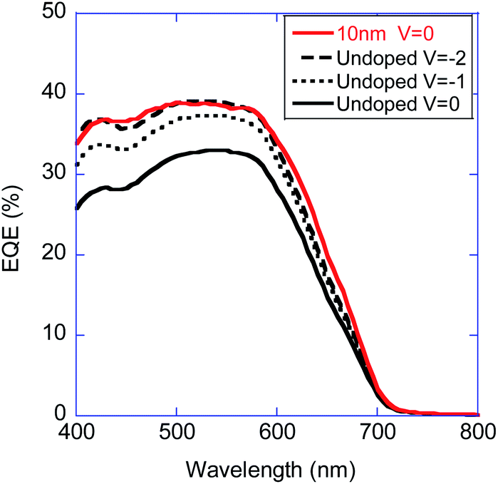 | ||
| Fig. 12 Measured external quantum efficiency as a function of excitation wavelength and using low light intensity for the undoped (reference) device for three bias levels. V = 0 (full line), V = −1 (dotted), and V = −2 (dashed). Also shown in red is the EQE at V = 0 for the device with the doped layer 10 nm away. | ||
Since the effect is at the device level and extends all the way between the p-type doped layer and the cathode, we can safely state that this effect is general and can be useful to both PHJ and BHJ devices. The 50% enhancement we measured is indeed due to our device starting point being very low; however, the overall analysis and our theoretical simulations suggest that at least 15% enhancement could be expected in BHJ solar cells.
To be more specific we analyzed the data recently reported for an 18% efficient cell.22 The open circuit voltage is at VOC = 0.86 V and at V = 0.7 V the cell loses 8% of the current compared to JSC. At the maximum power point VMPP = 0.85 VOC and JMPP = 0.89 JSC or JSC = 1.12 JMPP, taking the conservative approach and assuming that a top modulation-doped electron transport layer would not improve VOC and that the modulation doping would enhance JMPP only up to the present JSC value. Under these conditions the title of “18% efficiency…” would be replaced by “Above 20% efficiency…”, making it clear that even 12% is significant when you approach the fundamental limit.23,24
Conflicts of interest
There are no conflicts to declare.Acknowledgements
This research was supported by the Israel Science Foundation (grant no. 488/16) and Adelis Foundation for renewable energy research within the framework of the Grand Technion Energy Program (GTEP). H. S. acknowledges the support from the Technion Ollendorff Minerva Center. We thank Dr Laura Popilevsky and Yaron Kaufman for the cross-sectional SEM. We thank Dr Tatyana Kravchuk for the ToF-SIMS analysis and Dr Guy Ankonina for the ellipsometry. Part of the device fabrication process was performed at the Technion micro-nano fabrication and printing unit (MNF&PU).References
- N. K. Elumalai and A. Uddin, Energy Environ. Sci., 2016, 9, 391–410 Search PubMed.
- K. Vandewal, K. Tvingstedt, A. Gadisa, O. Inganäs and J. V. Manca, Phys. Rev. B, 2010, 81, 125204 Search PubMed.
- M. Azzouzi, T. Kirchartz and J. Nelson, Trends Chem., 2019, 1, 49–62 Search PubMed.
- A. Weu, T. R. Hopper, V. Lami, J. A. Kreß, A. A. Bakulin and Y. Vaynzof, Chem. Mater., 2018, 30, 2660–2667 Search PubMed.
- W. Peter, Physics of Solar Cells, Wiley, 2005 Search PubMed.
- M.-A. Pan, T.-K. Lau, Y. Tang, Y.-C. Wu, T. Liu, K. Li, M.-C. Chen, X. Lu, W. Ma and C. Zhan, J. Mater. Chem. A, 2019, 7, 20713–20722 Search PubMed.
- M. Schwarze, K. S. Schellhammer, K. Ortstein, J. Benduhn, C. Gaul, A. Hinderhofer, L. Perdigón Toro, R. Scholz, J. Kublitski, S. Roland, M. Lau, C. Poelking, D. Andrienko, G. Cuniberti, F. Schreiber, D. Neher, K. Vandewal, F. Ortmann and K. Leo, Nat. Commun., 2019, 10, 2466 Search PubMed.
- X. Liu, B. P. Rand and S. R. Forrest, Trends Chem., 2019, 1, 815–829 Search PubMed.
- A. W. Kohn, D. P. McMahon, S. Wen and T. Van Voorhis, J. Phys. Chem. C, 2017, 121, 26629–26636 Search PubMed.
- S. M. Menke, A. Cheminal, P. Conaghan, N. A. Ran, N. C. Greehnam, G. C. Bazan, T.-Q. Nguyen, A. Rao and R. H. Friend, Nat. Commun., 2018, 9, 277 Search PubMed.
- S. N. Hood and I. Kassal, J. Phys. Chem. Lett., 2016, 7, 4495–4500 Search PubMed.
- D. Liraz, P. Cheng, Y. Yang and N. Tessler, Sustainable Energy Fuels, 2020, 4, 760–771 Search PubMed.
- B. A. Gregg, J. Phys. Chem. Lett., 2011, 2, 3013–3015 Search PubMed.
- D. A. Vithanage, A. Devižis, V. Abramavičius, Y. Infahsaeng, D. Abramavičius, R. C. I. MacKenzie, P. E. Keivanidis, A. Yartsev, D. Hertel, J. Nelson, V. Sundström and V. Gulbinas, Nat. Commun., 2013, 4, 2334 Search PubMed.
- K. Vandewal, Annu. Rev. Phys. Chem., 2016, 67, 113–133 Search PubMed.
- A. A. Bakulin, A. Rao, V. G. Pavelyev, P. H. M. van Loosdrecht, M. S. Pshenichnikov, D. Niedzialek, J. Cornil, D. Beljonne and R. H. Friend, Science, 2012, 335, 1340–1344 Search PubMed.
- C. Göhler, A. Wagenpfahl and C. Deibel, Adv. Electron. Mater., 2018, 4, 1700505 Search PubMed.
- R. A. Marsh, J. M. Hodgkiss and R. H. Friend, Adv. Mater., 2010, 22, 3672–3676 Search PubMed.
- D. Veldman, Ö. İpek, S. C. J. Meskers, J. Sweelssen, M. M. Koetse, S. C. Veenstra, J. M. Kroon, S. S. van Bavel, J. Loos and R. A. J. Janssen, J. Am. Chem. Soc., 2008, 130, 7721–7735 Search PubMed.
- P. Song, Y. Li, F. Ma and M. Sun, J. Mater. Chem. C, 2015, 3, 4810–4819 Search PubMed.
- Y. Chang, T.-K. Lau, M.-A. Pan, X. Lu, H. Yan and C. Zhan, Mater. Horiz., 2019, 6, 2094–2102 Search PubMed.
- Q. Liu, Y. Jiang, K. Jin, J. Qin, J. Xu, W. Li, J. Xiong, J. Liu, Z. Xiao, K. Sun, S. Yang, X. Zhang and L. Ding, Science Bulletin, 2020, 65, 272–275 Search PubMed.
- R. A. J. Janssen and J. Nelson, Adv. Mater., 2013, 25, 1847–1858 Search PubMed.
- P. Cheng, G. Li, X. Zhan and Y. Yang, Nat. Photonics, 2018, 12, 131–142 Search PubMed.
- M. Mirsafaei, A. H. Fallahpour, P. Lugli, H.-G. Rubahn, J. Adam and M. Madsen, Sci. Rep., 2017, 7, 5300 Search PubMed.
- N. Tessler, J. Appl. Phys., 2015, 118, 215501 Search PubMed.
- B. Lüssem, M. Riede and K. Leo, Phys. Status Solidi A, 2013, 210, 9–43 Search PubMed.
- Y. Kazama, K. Seki, W.-Y. Kim, S. Yamanaka, M. Konagai and K. Takahashi, Jpn. J. Appl. Phys., Part 1, 1989, 28, 1160–1164 Search PubMed.
- K. Higuchi, K. Tabuchi, K. S. Lim, M. Konagai and K. Takahashi, Jpn. J. Appl. Phys., Part 1, 1991, 30, 1635–1640 Search PubMed.
- X.-Q. Liu, C. M. Fetzer and D. C. Law, US Pat., 2013/0220407 A1, 2013.
- H. F. Lu, L. Fu, G. Jolley, H. H. Tan and C. Jagadish, Improved performance of InGaAs/GaAs quantum dot solar cells using Si-modulation doping, COMMAD 2012, 2012, pp. 127–128 Search PubMed.
- P. Lam, S. Hatch, J. Wu, M. Tang, V. G. Dorogan, Y. I. Mazur, G. J. Salamo, I. Ramiro, A. Seeds and H. Liu, Nano Energy, 2014, 6, 159–166 Search PubMed.
- E. v. Hauff, E. d. Como and S. Ludwigs, Adv. Polym. Sci., 2017, 272, 109–138 Search PubMed.
- Y. Lin, Y. Firdaus, M. I. Nugraha, F. Liu, S. Karuthedath, A.-H. Emwas, W. Zhang, A. Seitkhan, M. Neophytou, H. Faber, E. Yengel, I. McCulloch, L. Tsetseris, F. Laquai and T. D. Anthopoulos, Adv. Sci., 2020, 7, 1903419 Search PubMed.
- D. Zhang, J. Wang, X. Zhang, J. Zhou, S.-U. Zafar, H. Zhou and Y. Zhang, J. Mater. Chem. C, 2020, 8, 158–164 Search PubMed.
- O. Magen and N. Tessler, J. Appl. Phys., 2017, 121, 195502 Search PubMed.
- P. Peter, Y. Aharon and R. F. Stephen, J. Appl. Phys., 2003, 93, 3693–3723 Search PubMed.
- K. Nakano and K. Tajima, Adv. Mater., 2017, 29, 1603269 Search PubMed.
- D. Cheyns, J. Poortmans, P. Heremans, C. Deibel, S. Verlaak, B. P. Rand and J. Genoe, Phys. Rev. B, 2008, 77, 165332 Search PubMed.
- C. Weichsel, L. Burtone, S. Reineke, S. I. Hintschich, M. C. Gather, K. Leo and B. Lüssem, Phys. Rev. B, 2012, 86, 075204 Search PubMed.
- H. Shekhar, O. Solomeshch, D. Liraz and N. Tessler, Appl. Phys. Lett., 2017, 111, 223301 Search PubMed.
- D. Liraz, H. Shekhar, L. Tzabari and N. Tessler, J. Phys. Chem. C, 2018, 122, 23271–23279 Search PubMed.
- H. Shekhar, V. Lami, O. Solomeshch, A. Fenigstein, L. Tomer, L. Becky, Y. Vaynzof and N. Tessler, Org. Electron., 2019, 67, 1–9 Search PubMed.
- O. Solomeshch, Y. J. Yu, A. A. Goryunkov, L. N. Sidorov, R. F. Tuktarov, D. H. Choi, J. I. Jin and N. Tessler, Adv. Mater., 2009, 21, 4456–4460 Search PubMed.
- A. F. Paterson, N. D. Treat, W. Zhang, Z. Fei, G. Wyatt-Moon, H. Faber, G. Vourlias, P. A. Patsalas, O. Solomeshch, N. Tessler, M. Heeney and T. D. Anthopoulos, Adv. Mater., 2016, 28, 7791–7798 Search PubMed.
- J. Li, C. W. Rochester, I. E. Jacobs, S. Friedrich, P. Stroeve, M. Riede and A. J. Moulé, ACS Appl. Mater. Interfaces, 2015, 7, 28420–28428 Search PubMed.
- N. Rappaport, O. Solomesch and N. Tessler, J. Appl. Phys., 2005, 98, 033714 Search PubMed.
- N. Tessler and N. Rappaport, J. Appl. Phys., 2004, 96, 1083–1087 Search PubMed.
- L. Tzabari, J. Wang, Y.-J. Lee, J. W. P. Hsu and N. Tessler, J. Phys. Chem. C, 2016, 120, 10146–10155 Search PubMed.
- L. Tzabari, V. Zayats and N. Tessler, J. Appl. Phys., 2013, 114, 154514 Search PubMed.
- L. Tzabari and N. Tessler, J. Appl. Phys., 2011, 109, 064501 Search PubMed.
- P. Nils-Krister, A. Hans and I. Olle, J. Appl. Phys., 2005, 97, 034503 Search PubMed.
- Y. Liu, B. Nell, K. Ortstein, Z. Wu, Y. Karpov, T. Beryozkina, S. Lenk, A. Kiriy, K. Leo and S. Reineke, ACS Appl. Mater. Interfaces, 2019, 11, 11660–11666 Search PubMed.
- B. Nell, K. Ortstein, O. V. Boltalina and K. Vandewal, J. Phys. Chem. C, 2018, 122, 11730–11735 Search PubMed.
- M. L. Tietze, J. Benduhn, P. Pahner, B. Nell, M. Schwarze, H. Kleemann, M. Krammer, K. Zojer, K. Vandewal and K. Leo, Nat. Commun., 2018, 9, 1182 Search PubMed.
Footnote |
| † Electronic supplementary information (ESI) available. See DOI: 10.1039/d0se00836b |
| This journal is © The Royal Society of Chemistry 2020 |