
 Open Access Article
 This Open Access Article is licensed under a
 Creative Commons Attribution 3.0 Unported Licence
In situ fabrication of dendritic tin-based carbon nanostructures for hydrogen evolution reaction†
Oluwafunmilola
Ola
*a,
Yu
Chen
b,
Kunyapat
Thummavichai
 bc and
Yanqiu
Zhu
b
bc and
Yanqiu
Zhu
b
aFaculty of Engineering, The University of Nottingham, University Park, Nottingham, NG7 2RD, UK. E-mail: Oluwafunmilola.Ola@nottingham.ac.uk; Tel: +44 (0)1157 487264
bCollege of Engineering, Mathematics and Physical Sciences, University of Exeter, EX4 4QF, UK
cKey Laboratory of New Processing Technology for Nonferrous Metals and Materials, Ministry of Education, School of Resources, Environment and Materials, Guangxi University, Nanning, China
First published on 12th August 2020
Abstract
In this work, dendritic tin-based carbon (Sn/C) nanostructures with four different morphologies were synthesized by a facile two-step carbonization and chemical vapor deposition method and were then evaluated for their performance in hydrogen evolution reaction. The Sn/C dendrites are approximately 0.5–4.5 μm in length, each having secondary branches in different directions. The four morphologies of the Sn/C dendrites namely nanoflowers (Sn_NCF1), nanospheres (Sn_NCF2), nanocubes (Sn_NCF3) and nanocuboids (Sn_NCF4), behave differently in their electrochemical performance, with Sn_NCF2 and Sn_NCF1 performing better. Sn_NCF2 demonstrates optimal HER performance compared to other Sn based samples with onset potential and overpotential of 100 and 260 mV, respectively. The higher electrochemical surface area observed in Sn_NCF2 originated from the presence of more catalytic sites which contributed to the enhanced HER activity and better current density, against other Sn-based samples. In addition to the improved HER performance, Sn_NCF2 demonstrates excellent stability with less than 6% degradation of its initial current after operating for over 8 h in acidic media.
Introduction
New electrocatalyst materials have been intensively investigated in recent years for fuel cells and water splitting applications, due to the prospect of generating pure hydrogen which represents a clean and sustainable energy carrier that can potentially substitute fossil fuels. However, electrochemical water splitting via hydrogen evolution reaction (HER) is limited by the sluggish kinetics and large overpotential of these electrochemical reactions. Platinum and its alloys are the key electrocatalysts for hydrogen evolution reaction at the cathode, however the scarcity and cost of these materials limit their commercial applications.1 Great interest has been focused on the development of alternative electrocatalysts with high catalytic reactivity through the control of material morphology (including dimensionality and shape), structural parameters and chemical compositions. Graphitic carbon nitride (g-C3N4), a two-dimensional (2D) material consisting of carbon (C) and nitrogen (N) arranged in tri-s-triazine or triazine units, has attracted increasing interest as a promising, metal-free alternative to explore their potentials for water splitting, CO2 reduction and metal–air batteries, due to its tunable chemistry, high thermal and chemical stability, low cost and non-toxicity.2,3 Its electrocatalytic performance is limited by its fast charge recombination and low conductivity.4To counter these drawbacks, nanostructured g-C3N4 has been doped with heteroatoms, coupled with a co-catalyst for the formation of heterojunctions, in order to improve the charge separation and transport, as well as hydrogen production efficiency.5 The decoration or doping with metal nanoparticles such as copper, tin etc. on the surface or insertion into the structure of g-C3N4 can improve the metal–support interaction, increase metal disparity, enhance surface area, and increase the synergistic catalytic effect, so that prolonged lifetime of charge carriers required for HER can be achieved.6–11 Therefore, the design and synthesis of well-controlled shape and size of low-cost metal-doped g-C3N4-based nanostructures are of importance for improving their performance, especially their electrocatalysis performance for HERs.
We report a facile chemical vapor deposition method for the preparation of a novel three dimensional (3D) electrocatalyst consisting of dendritic tin-based nanostructures on a g-C3N4 support (Sn/C). The effect of Sn precursor concentration on the physicochemical and electrochemical properties of the Sn/C nanostructures will be investigated. We will demonstrate that the resulting dendritic nanostructured electrocatalysts exhibit excellent HER catalytic activity.
Experimental
Preparation of dendritic Sn/C nanostructures
Dendritic Sn/C nanostructures were grown via a two-step process which consists of carbonization of formaldehyde-melamine–sodium bisulfite copolymer (Basotect) from room temperature to 1200 °C at heating rate of 5 °C min−1 under inert gas flow rate of 100 ml min−1 (Fig. S1†), followed immediately by a chemical vapor deposition of tin chloride (SnCl2)–acetone (C3H6O) solution (Sigma Aldrich). Different mass concentrations (0.005 g ml−1, 0.01 g ml−1, 0.05 g ml−1 and 0.1 g ml−1) of SnCl2–C3H6O precursor were introduced into the furnace, at an injection speed of 0.3 ml min−1 at a reaction temperature of 950 °C for 2 h. The resulting samples prepared with SnCl2–C3H6O concentrations of 0.005 g ml−1, 0.01 g ml−1, 0.05 g ml−1 and 0.1 g ml−1 were referred to as Sn_NCF1, Sn_NCF2, Sn_NCF3 and Sn_NCF4, respectively.Characterization and electrochemical testing
The morphologies of the dendritic Sn/C nanostructures derived from different precursor concentrations were examined using a scanning electron microscope (Hitachi S3200N, Oxford instrument – SEM-EDS) and JEOL-2100 high-resolution transmission electron microscope (HR-TEM), respectively. Three-dimensional (3D) images were recorded with an X-Tek Benchtop 160Xi CT machine. The Brunauer–Emmett–Teller (BET) specific surface area of the samples and pore size distribution were measured using the Micromeritics ASAP 2020. A Renishaw benchtop Raman system, with 532 nm excitation wavelength and 2400 l mm−1 grating, was used to acquire the Raman spectra of all samples. X-ray diffraction were recorded on a Bruker D8 Advance diffractometer (operated at 40 kV, 40 mA), with a Cu Kα radiation, at a step size of 0.02° and a dwell time of 1 s. Surface chemical analysis was conducted on a Kratos Axis Ultra system with a monochromated Al Kr X-ray source, operated at 10 mA emission current and 15 kV anode potential. A CHI-760D workstation coupled with a rotating disk electrode (RDE) system consisting of Ag/AgCl/KCl, platinum wire and glassy carbon electrode (GCE) covered with the catalyst ink as the reference, counter and working electrodes respectively, was used to evaluate the electrocatalytic activity of the samples for HER. Electrochemical measurements, i.e. cyclic voltammograms, linear sweep voltammograms and impedance spectroscopy, were carried out in a 0.5 M H2SO4 (Sigma Aldrich) electrolyte solution, at different potentials and scan rates varying from 0 to −0.8 V and 10–100 mV, respectively. The frequency range and voltage amplitude of 100 kHz to 0.1 Hz and 5 mV was used for impedance measurements, respectively. The experimentally measured potential versus Ag/AgCl, EAg/AgCl, was calibrated with respect to the RHE (reversible hydrogen electrode), ERHE, according to the Nernst equation; ERHE = EAg/AgCl + E0Ag/AgCl + 0.059pH (at 25 °C), where E0Ag/AgCl = 0.1976 V at 25 °C. The acquired HER experimental values were generated in 0.5 M H2SO4 solution (pH = 0). The iR compensation was applied to all polarization curves due to the effect of ohmic resistance on intrinsic catalytic activity. The iR compensation was automatically applied by the CHI 660E software with a compensation level of 95%. The electrochemical active surface areas of the samples were evaluated by measuring the double layer capacitance obtained from a fitting of the difference in current densities versus the scan rates.Results and discussion
Structural and physicochemical properties
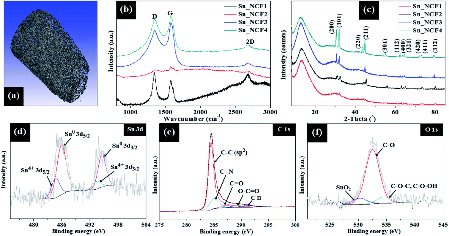
SEM and HR-TEM images of the Sn/C prepared with different mass concentrations of SnCl2–C3H6O precursor are shown in Fig. 1. With increasing precursor concentration, the morphology of the samples changed from nanoflowers (Sn_NCF1), nanospheres (Sn_NCF2), nanocubes (Sn_NCF3) to nanocuboids (Sn_NCF4) of a few to hundreds of micrometres in length and diameters. At the lowest precursor concentration of 0.005 g ml−1 (Sn_NCF1), individual particles, 0.1 um in diameter, were stacked together to form aggregates of three-dimensional (3D) Sn/C nanoflowers, as shown in Fig. 1a. As the precursor concentration increased to 0.01 g ml−1 (Sn_NCF2), larger nano- and micro-sized spheres of varying diameters were observed (Fig. 1b). | ||
| Fig. 1 Morphologies of the dendritic Sn/C nanostructures: (a) Sn_NCF1; (b) Sn_NCF2; (c) Sn_NCF3; and (d) Sn_NCF4. | ||
For Sn_NCF3 prepared with 0.05 g ml−1, nanocubes with well-defined edges and corners and nanorods of different lengths ranging from 200 nm to a few micrometres were observed (Fig. 1c). At the highest concentration of 0.1 g ml−1 (Sn_NCF4), nanocuboids were observed (Fig. 1d). Elemental mapping images from the energy dispersive spectroscopy under scanning TEM mode confirmed that the dendritic nanostructures were primarily composed of Sn and C, where Sn was uniformly distributed in the framework (Fig. S2†). The HR-TEM images displayed in Fig. 2 showed that the Sn/C dendrites were approximately 0.5–4.5 μm in length, with secondary branches grown towards different directions. In Sn_NCF3 and 4, the asymmetric secondary branches also possessed integral tertiary leaves to form hierarchical Sn/C nanostructures.
 | ||
| Fig. 2 Low magnification TEM images of dendritic Sn/C nanostructured samples: (a) Sn_NCF1; (b) Sn_NCF2; (c) Sn_NCF3; (d) Sn_NCF4; (e) high resolution TEM image and (f) SAED pattern of Sn_NCF4. | ||
The HR-TEM image in Fig. 2e shows the lattice fringes which exhibits a d-spacing of 2.9 Å, corresponding to the (200) plane of the tetragonal phase of Sn. The selected area electron diffraction (SAED) pattern in Fig. 2f shows the ring pattern and diffraction spots, which are indexed to the (002), (101), (200), (211) and (220) crystalline planes of the graphitic nitride, g-C3N4, and single crystalline tetragonal β-Sn, respectively.12–14 The SAED results in Fig. 2f are consistent with the findings obtained from the XRD and XPS results that will be described below. The BET specific surface area and total pore volume of the samples are listed in Table S1.† The surface area of the samples increased compared to g-C3N4, and slightly decreases with increased Sn concentration. Also, the samples possess a broad pore distribution ranging from 3 to 25 nm which is mainly centred around 3.2 nm (Fig. S3†). The 3-D feature of the sample in X, Y and Z directions was also confirmed by the micro-CT analysis, and the result was shown in Fig. 3a. The graphitization degrees of the Sn/C samples were investigated by Raman spectroscopy (Fig. 3b), in which the peaks at 1340–1348 cm−1, 1572–1581 cm−1 and 2674–2691 cm−1 represent the D band, G band and 2D band, respectively. The D band also known as the defect band originates from hybridized vibrational mode associated with graphene edges while the G band represents the Raman E2g vibrational mode linked to stretching of the C–C bond, respectively. The Raman 2D band represents the overtone of the D band due to second order Raman scattering of an in-plane transverse optical mode close to the zone boundary K point in graphene.15 The intensity ratio of Raman D and G bands, ID/IG, provides a quantitative measure of the edge plane exposure and structural defect sites. A change in frequency and the ID/IG ratios was observed for the samples prepared with varying SnCl2–C3H6O precursor concentrations. The Raman G bands of Sn/C samples _NCF4 was red-shifted compared to g-C3N4. For example, the G band of Sn_NCF4 was red-shifted to 1572 cm−1, in comparison to 1595 cm−1 for g-C3N4 support, implying the formation of Sn/C hybrids.9 The shift in frequency of the D and G band observed for these samples are linked to the structural defect sites caused by grain boundaries, vacancies and incorporation of Sn atoms into the g-C3N4 layers. The ID/IG ratio decreased from 1.18 to 0.86 for Sn_NCF1 and Sn_NCF3, respectively, whilst being 0.94 for sample Sn_NCF4. Similar trend was also observed for the I2D/IG ratios, where ratio decreased to 0.27 for Sn_NCF3 and increased to 0.5 for Sn_NCF4, benchmarked against 1.7 and 0.8 for Sn_NCF1 and Sn_NCF2, respectively.
 | ||
| Fig. 3 (a) Micro-CT image of Sn_NCF2; (b) Raman spectrum; (c) XRD pattern; XPS spectra of: (d) Sn 3d, (e) C 1s and (f) O 1s for Sn_NCF2. | ||
The crystal and phase structures of the dendritic Sn/C samples were further characterized by XRD, and the results are presented in Fig. 3c. The XRD patterns of all samples exhibit sharp diffraction peaks, corresponding to the (200), (101), (220), (211) and (301) planes (JCPDS card no. 04-0673), indicating that the dendrites consist of tetragonal single crystals of Sn. A broad peak occurred in all samples at 2θ = 13.1° can be assigned to the g-C3N4. With increasing concentrations of SnCl2–C3H6O from 0.005–0.1 g ml−1, the intensity of this broad peak became stronger which indicates better growth and crystallization of the g-C3N4 phase. The average crystallite size (D) of the dendritic Sn was estimated from the full width at half maximum intensity (FWHM), β, for the Sn (101) peak using the Scherrer's equation; D = 0.94λ/β![[thin space (1/6-em)]](https://www.rsc.org/images/entities/char_2009.gif) cosθ; in which θ and λ are the Bragg's angle and X-ray wavelength (1.54 Å). The average D values are 61.4 nm, 111.7 nm, 188.6 nm and 215.3 nm for samples Sn_NCF1, Sn_NCF2, Sn_NCF3 and Sn_NCF4, respectively. With increasing the precursor concentration, smaller Sn crystals aggregated to form larger crystals, as observed for sample Sn_NCF4. This is also supported by the TEM results. The XRD pattern showed no evidence of diffraction patterns of the tin oxides, revealing that tetragonal Sn was the dominant crystalline phase forming the dendrites during the second stage of CVD. These XRD results confirmed that the samples were indeed Sn nanoparticles grown on top of the struts of the g-C3N4 matrix. The surface chemical states of the samples were further analysed by X-ray photoelectron spectroscopy (XPS). The high resolution XPS spectra shown in Fig. 3d–f confirmed the presence of Sn, C and O, an indication of the formation of tin oxide on the surface. It is possible that a thin amorphous oxide layer was formed on the Sn crystal surface, due to part oxidization, which was undetectable by XRD owing to the minute amounts. In Fig. 3d, the high resolution XPS spectra of Sn 3d can be deconvoluted into 3d5/2 peak and 3d3/2 peak, which can be fitted into two pairs of peaks at 485.9/494.6 eV and 484.6/495.9 eV, corresponding to Sn and Sn4+, respectively. The C 1s spectrum in Fig. 3e exhibits five main peaks, with the main contribution from binding energy at 284.5 eV that is corresponding to the sp2 C–C bonds. Other peaks at 285 eV, 287.6 eV, 289.4 eV and 291.2 eV are linked to C
cosθ; in which θ and λ are the Bragg's angle and X-ray wavelength (1.54 Å). The average D values are 61.4 nm, 111.7 nm, 188.6 nm and 215.3 nm for samples Sn_NCF1, Sn_NCF2, Sn_NCF3 and Sn_NCF4, respectively. With increasing the precursor concentration, smaller Sn crystals aggregated to form larger crystals, as observed for sample Sn_NCF4. This is also supported by the TEM results. The XRD pattern showed no evidence of diffraction patterns of the tin oxides, revealing that tetragonal Sn was the dominant crystalline phase forming the dendrites during the second stage of CVD. These XRD results confirmed that the samples were indeed Sn nanoparticles grown on top of the struts of the g-C3N4 matrix. The surface chemical states of the samples were further analysed by X-ray photoelectron spectroscopy (XPS). The high resolution XPS spectra shown in Fig. 3d–f confirmed the presence of Sn, C and O, an indication of the formation of tin oxide on the surface. It is possible that a thin amorphous oxide layer was formed on the Sn crystal surface, due to part oxidization, which was undetectable by XRD owing to the minute amounts. In Fig. 3d, the high resolution XPS spectra of Sn 3d can be deconvoluted into 3d5/2 peak and 3d3/2 peak, which can be fitted into two pairs of peaks at 485.9/494.6 eV and 484.6/495.9 eV, corresponding to Sn and Sn4+, respectively. The C 1s spectrum in Fig. 3e exhibits five main peaks, with the main contribution from binding energy at 284.5 eV that is corresponding to the sp2 C–C bonds. Other peaks at 285 eV, 287.6 eV, 289.4 eV and 291.2 eV are linked to C![[double bond, length as m-dash]](https://www.rsc.org/images/entities/char_e001.gif) N, CO, O–CO and C π, respectively.16
N, CO, O–CO and C π, respectively.16
The π* edge (285, 287.6 eV) and σ* edge (291.2 eV) peaks are assigned to graphitic, defective and sp3 carbon species, respectively. These π* and σ* resonances are linked to the core-level electron transitions between the unoccupied antibonding π* and σ* orbitals. The σ* excitation indicates the formation of new sp3 carbon species, generated via the in situ growth of nanoscale g-C3N4 domains on the Sn surfaces. This result appears to support that chemical coupling was induced between the g-C3N4 and Sn species during the CVD process. Meanwhile, the O 1s spectrum (Fig. 2f) contains 3 components: the O–Sn4+ species (530.3 eV), C–O bond (532.5 eV) and C–OH bond (534.3 eV). The XPS spectra demonstrate that the dendritic structures comprised of metallic Sn, g-C3N4 and minute amounts of amorphous SnO2.
Electrochemical properties
The electrocatalytic HER performances of the dendritic Sn/C nanostructures, against 20 wt% Pt/C standard electrode, were assessed in the same 0.5 M H2SO4 electrolyte solution. By comparing the magnitude of current density recorded in the polarization curves, highlighted in Fig. 4a, an increased HER activity and current density were observed, in the order of Sn_NCF4, Sn_NCF3, Sn_NCF1, Sn_NCF2 and 20 wt% Pt/C. When the Sn precursor concentration was between 0.005–0.01 g ml−1, the HER performance was improved, but above 0.01 g ml−1, the performance dropped. The improved performance was due to the presence of more active sites and the rapid electron transfer at the solid–liquid interface, as observed from electrochemical impedance spectroscopy (EIS) that will be described below. In addition, the dendritic structure can provide better dispersibility and larger reaction areas. The carbon-based support could also synergize the HER process by promoting faster reactant adsorption and product desorption. The reduced HER performance for Sn_NCF3 and Sn_NCF4 could be linked to excessive amount of Sn precursor being absorbed on existing Sn nanoparticles during growth and covering active sites to generate larger Sn nanoparticles, as observed in the increased crystallite sizes by XRD. The Sn_NCF2 electrode exhibited the best HER activity in 0.5 M H2SO4 solution and required an overpotential (η10) of 260 mV to achieve 10 mA cm−2. As deduced from Fig. 4a, this overpotential was higher than that of the 20 wt% Pt/C (50 mV) electrode, and lower than samples Sn_NCF1 (302 mV), Sn_NCF3 (325 mV) and Sn_NCF4 (478 mV). More importantly, the catalytic current density of sample Sn_NCF2 increased rapidly with further cathodic polarization beyond 10 mA cm−2, to attain current densities of 90 and 180 mA cm−2 at overpotentials of 315 and 340 mV, respectively. | ||
| Fig. 4 (a) Polarization curve, and (b) Tafel slope of g-C3N4, Sn_NCF1, Sn_NCF2, Sn_NCF3, Sn_NCF4 and 20 wt% Pt/C; (c) double-layer charging currents as a function of scan rate, and (d) Nyquist plots of Sn_NCF1, Sn_NCF2, Sn_NCF3 and Sn_NCF4 recorded at 350 mV overpotential. | ||
The Tafel slope reflects the kinetics of HER and is shown in Fig. 4b. The Tafel slope of Sn_NCF2 was 53 mV dec−1, which was lower than those of Sn_NCF2 (62 mV dec−1), Sn_NCF1 (72 mV dec−1) and Sn_NCF4 (97 mV dec−1), and higher than that of 20 wt% Pt/C (17 mV dec−1). The reactions proposed for HER in an acidic medium consists of three mechanisms namely Volmer, Heyrovsky and Tafel which are associated with the discharge process, chemical desorption and recombination, respectively. Since the Tafel slope values of the Sn dendritic nanostructures fell within the range of 40–120 mV dec−1, the Sn dendritic samples therefore underwent Volmer–Heyrovsky mechanisms, so the initial adsorption of protons from the acid electrolyte to form adsorbed H (Had) occurred followed by the reaction of a solvated proton with one adsorbed surface hydrogen to H2.1 The HER mechanism of the present dendritic samples is different to that of Pt/C which showed a Tafel slope of 17 mV dec−1, indicative of a Volmer–Tafel mechanism.17 Hence, the lowest Tafel value of sample Sn_NCF2 compared with other Sn-based samples indicated the occurrence of a faster electron transfer during HER. The rate limiting step for the dendritic Sn/C nanostructures was the electrochemical discharge process based on the Volmer–Heyrovsky mechanism. The onset potential (to reach 0.5 mA cm−2), overpotential (η10) and Tafel slope are the key parameters used in evaluating the HER performance of a material. Sample Sn_NCF2 exhibited impressive onset potential, overpotential (η10) and Tafel slope of 100 mV, 260 mV and 53 mV dec−1, respectively, which exceeded several values reported recently for g-C3N4-based electrocatalysts, especially in terms of the onset potential and current density (Table S2†).9,11,18,19 The number of catalytic active sites for electrocatalysts is linked to the catalytic current density, which was extrapolated from the cyclic voltammetry (CV) curves obtained at different scan rates and from the double layer capacitance (Cdl), as shown in Fig. S4† and 4c. The electrochemical active surface area (ESCA) of sample Sn_NCF2 was 26.2 mF cm−2, which was larger than those of samples Sn_NCF1 (10.5 mF cm−2), Sn_NCF3 (5.5 mF cm−2) and Sn_NCF4 (4.9 mF cm−2). The higher ESCA observed in Sn_NCF2 was originated from the presence of more catalytic sites which contributed to the enhanced HER activity and better current density, against other Sn-based samples. The electrochemical impedance spectroscopy (EIS) was conducted to study the electrocatalytic kinetics of HER for all samples. The Rct of Sn_NCF2 was lower than values of other samples at the potential of −0.3 V versus RHE, suggesting a faster electron transfer rate and higher cathodic efficiency for sample Sn_NCF2, which is favourable for HER.20
To further evaluate the stability of the present dendritic Sn/C samples, cyclic measurements of the polarization and chronoamperometric curves were obtained and presented in Fig. 5a. The cyclic measurements of the polarization curves of bare structure of g-C3N4 before CVD growth with SnCl2–C2H5O was also presented in Fig. S5† for comparison. As shown in Fig. 5a and S5†, an activity retention of ∼95% was observed up to 1000 cyclic voltammetry cycles between 0.3 and −0.65 V. The chronoamperometric curve recorded at −0.25 V in Fig. 5b also showed a marginal attenuation in the catalytic activity, cathodic current and current density, after 8 hours of testing. The SEM (Fig. 5c) and XRD (Fig. 5d) characterization of post-testing sample of Sn_NCF2 after 8 hours also showed no changes in the morphology or structure, indicative high stability for the sample. XPS studies of sample Sn_NCF2 before and after the electrochemical testing (Fig. S6†) showed similar peaks, however a change in relative proportion of Sn0 and Sn4+ was observed, which is due to the oxidation of Sn species with increasing HER cycles. In summary, these structural analyses further confirmed that sample Sn_NCF2 exhibited excellent stability for HER. Further work will focus on combining experimental data with first principles theoretical tools such as density of state and electronic structure calculations (i.e. density functional theory) to gain further understanding of the electrochemical properties.
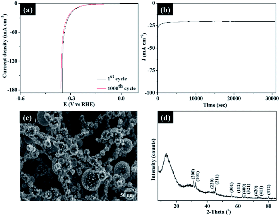 | ||
| Fig. 5 (a) Polarization curve of Sn_NCF2 showing electrochemical stability before and after 1000 cycles; (b) durability test by chronoamperometry curve of Sn_NCF2 at −0.25 V; (c) SEM image of Sn_NCF2 after 8 hours of testing, and (d) XRD image of Sn_NCF2 after 8 hours of testing. | ||
Conclusions
Dendritic Sn/C nanostructures of different morphologies and compositions were successfully prepared and tested for their HER performance. The tin-based carbon (Sn/C) dendrites were approximately 0.5–4.5 μm in length, with secondary branches grown towards different directions. Sn was uniformly distributed in the g-C3N4 framework, and chemically bonded with the supporting matrix. The Sn/C dendrites with different morphologies namely nanoflowers (Sn_NCF1), nanospheres (Sn_NCF2), nanocubes (Sn_NCF3) and nanocuboids (Sn_NCF4) behave differently in their electrochemical performance. Among them, Sn_NCF2 presents spherical morphology and has the optimum HER performance with onset potential, overpotential (η10) and Tafel slope of 100 mV, 260 mV and 53 mV dec−1, respectively. Based on the EIS and ESCA measurements, the enhanced HER electrocatalytic activity of Sn_NCF2 is attributed to the chemical coupling between Sn and g-C3N4 which promotes proton adsorption by reducing adsorption kinetics, the higher electrochemically active surface area, and the faster electron transfer rate at the electrocatalyst/electrolyte interface. Sample Sn_NCF2 also exhibits excellent durability during long-term cycling in acidic environment. Moreover, the Sn/C dendritic nanostructures were prepared via a facile and scalable approach using low-cost precursors, and it is expected that this technique can be easily extended to the preparation of other metal-based electrocatalysts that can be explored for applications in fuel cells, solar cells, etc.Conflicts of interest
There are no conflicts to declare.Acknowledgements
O. Ola is grateful for the support from the Leverhulme Trust Early Career Fellowship, ECF-2018-376.References
- N. Dubouis and A. Grimaud, Chem. Sci., 2019, 10, 9165–9181 RSC.
- K. S. Lakhi, D. H. Park, K. A. Bahily, W. Cha, B. Viswanathan, J. H. Choy and A. Vinu, Chem. Soc. Rev., 2017, 46, 72–101 RSC.
- J. Duan, S. Chen, M. Jaroniec and S. Z. Qiao, ACS Nano, 2015, 9, 931–940 CrossRef CAS PubMed.
- C. Fettkenhauer, G. Clavel, K. Kailasam, M. Antonietti and D. Dontsova, Green Chem., 2015, 17, 3350–3361 RSC.
- H. Jiang, J. Gu, M. Liu, X. Qiu, L. Wang, W. Li, Z. Chen, X. Ji and J. Li, Energy Environ. Sci., 2019, 12, 322–333 RSC.
- Y. Zhu, D. Zhang, L. Gong, L. Zhang and Z. Xia, Front. Mater., 2019, 6, 16 CrossRef.
- M. Cao, X. Zhang, J. Qin and R. Liu, ACS Sustainable Chem. Eng., 2018, 6, 16198–16204 CrossRef CAS.
- M. Gao, D. Liu, H. Yang, H. Huang, Q. Luo, Y. Huang, X. F. Yu and P. K. Chu, J. Nanomater., 2019, 9, 568 CrossRef CAS PubMed.
- S. S. Shinde, A. Sami and J. H. Lee, J. Mater. Chem. A, 2015, 3, 12810–12819 RSC.
- M. B. Idris and S. Devaraj, J. Energy Storage, 2019, 26, 101032 CrossRef.
- R. C. P. Oliveira, M. Sevim, B. Sljukic, C. A. C. Sequeira, O. Metin and D. M. F. Santos, Catal. Today, 2019 DOI:10.1016/j.cattod.2019.09.006.
- M. Ramalingam, V. K. Ponnusamy and S. N. Sangilimuthu, Microchim. Acta, 2019, 186, 69 CrossRef PubMed.
- N. Arora and B. R. Jagirdar, Phys. Chem. Chem. Phys., 2014, 16, 11381–11389 RSC.
- R. Li, Y. Zhang and X. Sun, J. Mater. Res., 2013, 28, 969–975 CrossRef CAS.
- J.-B. Wu, M.-L. Lin, X. Cong, H.-N. Liu and P.-H. Tan, Chem. Soc. Rev., 2018, 47, 1822–1873 RSC.
- S. Kim, J. Kim, J. Lim, H. Lee, Y. Jun and D. Kim, J. Mater. Chem. C, 2014, 2, 6985–6990 RSC.
- Z. Chen, X. Duan, W. Wei, S. Wang and B.-J. Ni, J. Mater. Chem. A, 2019, 7, 14971–15005 RSC.
- Y. Ito, W. Cong, T. Fujita, Z. Tang and M. Chen, Angew. Chem., 2015, 127, 2159–2164 CrossRef.
- Y. Zheng, et al. , ACS Nano, 2014, 8, 5290–5296 CrossRef CAS PubMed.
- Y. Yang, H. Yang, C. Liang and X. Zhu, Int. J. Electrochem. Sci., 2018, 13, 7193–7205 CrossRef CAS.
Footnote |
| † Electronic supplementary information (ESI) available. See DOI: 10.1039/d0se00812e |
| This journal is © The Royal Society of Chemistry 2020 |