
Orientationally engineered 2D/3D perovskite for high efficiency solar cells†
Muhammad Sohail
Abbas
 ab,
Sabir
Hussain
cd,
Jinaqi
Zhang
b,
Boxin
Wang
b,
Chen
Yang
bc,
Zhen
Wang
be,
Zhixiang
Wei
bc and
Rashid
Ahmad
*a
ab,
Sabir
Hussain
cd,
Jinaqi
Zhang
b,
Boxin
Wang
b,
Chen
Yang
bc,
Zhen
Wang
be,
Zhixiang
Wei
bc and
Rashid
Ahmad
*a
aDepartment of Chemistry, University of Malakand, Chakdara, Dir-L, Pakistan. E-mail: rashmad@gmail.com
bCAS Key Laboratory of Nano Systems and Hierarchical Fabrication, CAS Center for Excellence in Nanoscience, National Center for Nanoscience and Technology, Beijing 100190, P. R. China
cUniversity of Chinese Academy of Sciences, Beijing 100049, P. R. China
dCAS Key Laboratory of Standardization and Measurement for Nanotechnology, CAS Center for Excellence in Nanoscience, National Center for Nanoscience and Technology, Beijing 100190, China
eDepartment of Chemistry, MOE Key Laboratory of Organic Optoelectronics and Molecular Engineering, Tsinghua University, Beijing 100084, P. R. China
First published on 15th October 2019
Abstract
Recently, the focus on perovskite solar cell researchers has shifted from 3D perovskites to hybrid 2D/3D multidimensional perovskite, in which a large cation is used as a spacer between the [PbX6]4− layers. 2D/3D perovskites are stable as compared to 3D ones but they suffer from inferior photovoltaic performance. Herein, we report a highly efficient anilinium based 2D/3D perovskite with improved PCE of 16%. We have utilized a better compositional management, which has resulted in a 2D/3D perovskite, in which a 2D layered perovskite An2PbI4 coherently exists with a bulk of 3D MAPbI3 perovskite periodically oriented in the vertical direction. This new 2D/3D perovskite has surpassed 3D MAPbI3 in terms of not only photovoltaic performance but also in PL emission, surface morphology, and surface potential.
1. Introduction
Organometal halide perovskite based solar cells came into the spot light when the first perovskite based solid state solar cell was reported with 9.7% efficiency in 2012.1 Since then, researchers have made tremendous progress in this field and as a result, efficiency of perovskite solar cells (PSC) has reached over 24%.2 As an intrinsic light absorbing material, these are important due to their high electron/hole productivity and mobility with carrier diffusion length of more than 100 nm.1 Such solar cell devices are easy to fabricate, cheap, and are almost free from any negative impact on humans or environment.1,3,4Generally, three-dimensional (3D) perovskite compounds have an ABX3 type chemical formula, where “A” is a monovalent cation that may be organic such as methyl ammonium CH3NH3+ (MA+) or formamidinium CH2(NH2)2+ (FA+), or inorganic such as caesium Cs+, while “B” represents a divalent metal ion Pb2+ or Sn2+ and “X” stands for a halide ion.5 The leading representatives of 3-dimensional perovskites are methylammonium lead triiodide (MAPbI3), formamidinium lead triiodide (FAPbI3), and CsPbI3. Despite their excellent optoelectronic properties, these materials lack durability and longer stability when exposed to heat, oxygen, ultra-violet (UV) radiation, and humidity of the environment.6–11 The most extensively studied perovskite, MAPbI3, is thermally unstable due to the volatile nature of the MA+ ion, which causes structural degradation at high temperature and moisture.9,12–17 Comparatively, FAPbI3 is better in terms of thermal stability but it is structurally unstable as it goes through a phase change from perovskite to non-perovskite phase at room temperature.18,19
To overcome these issues in 3D perovskite materials, a new emerging trend is the use of two-dimensional (2D) Ruddlesden–Popper layered phase perovskites. 2D perovskites have a general formula of M2(n)An−1BnX3n+1, where “M” is a cation, large in size and organic in nature, “A” represents smaller cations such as MA+ or FA+, and “n” is the number of 3D inorganic layers separating the organic layers. The “n” value may vary from 1 to ∞. When n = 1, we have pure 2D structure and when n = ∞ structure is completely 3D.9,20,21 2D perovskites are better in terms of thermal and structural stability but their photovoltaic performance is relatively low because of their wider band gap of about 2.5 eV and the charge transportation across inorganic layers is inhibited by the organic spacer.22–24
Currently, researchers have been focusing more on 2D/3D mixed dimensional or simply 2D/3D perovskites in addition to purely 3D perovskites. These 2D/3D perovskites factually combine the stability of 2D layered perovskite with excellent electron/hole carrier capabilities of 3D perovskite, giving rise to photovoltaically more efficient, robust, and ultra-stable devices. 2D/3D perovskites are well ahead of their 3D counterparts in terms of stability.23,25–28 Many larger cations have been tried in 2D/3D perovskites but butylammonium (BA+) and phenylethylammonium (PEA+) are the most explored large cations in 2D perovskites.23,28
Recently, Mora-Seró and Barea et al. investigated that 2D/3D perovskites containing anilinium ion as organic spacers provide better optoelectronic properties as compared to butylammonium based perovskites. They achieved a PCE of 5.94% (ref. 29) and PCE of 7.63% for 2D/3D perovskite An2(n)MAn−1PbnI3n+1 with a lower n value (n = 3 and 5) while using hot cost method for device fabrication.30 Anilinium based 2D/3D perovskites exhibit a higher photoemission, which also makes them better candidates to be explored and tried in other devices such as photodetectors and thermoelectric photodetectors, inject printers, and light emitting diodes (LEDS). Some other perovskites have also been applied in such devices.31–36
In this study, we have developed a method to add a layered 2D perovskite with a bulk of 3D MAPbI3 in such a way that it does not limit its photocurrent generation. This expected target of improved photovoltaic performance of MAPbI3 based 2D/3D perovskite was achieved by mixing a vertically oriented 2D layered perovskite with a bulk 3D perovskite. This is the latest strategy to obtain a 2D/3D heterostructure, in which a bulk 3D perovskite is coherently attached to a pure 2D phase perovskite (n = 1) having a periodically repeated vertical orientation. This new strategy has resulted in better photoconversion performance of the devices. Furthermore, we selected anilinium ion, which has been previously found to be a better large cation for multidimensional perovskites having free and polarizable π-electrons, and better photoconversion and photoemission characteristics as compared to other aliphatic and non-conjugated larger cations.29 We have used a more suitable composition of perovskite precursor solutions for 2D/3D hybrid perovskites in order to obtain a 2D/3D hetero-structure consisting of 3D MAPbI3 with seamless and vertical coherence of 2D (C6H5NH3)2PbI4 or (An2PbI4) perovskite. This 2D/3D heterostructured perovskite boosted the photovoltaic performance of MPbI3 and increased the PCE up to 16%. We have also explored the effect of FA+ and Cs+ ions' addition on this new perovskite.
2. Results and discussion
Film structure and characterization
To investigate the crystal structure with detailed insight of crystallinity of the MAPbI3 interlayers and to find out the resultant variations and expected orientation of the 2D perovskite, we preformed GIWAXS for the exploration of different perovskite films. GIWAXS patterns of both pristine perovskite and 2D/3D perovskite with anilinium iodide are given in Fig. 1. Fig. 1a shows the diffraction pattern for pure MAPbI3 film, suggesting a 3D perovskite structure with a random organisation of the crystals. Rings A–E, which correspond to miller indices 222, 220, 202, 111, and 110, respectively, confirm the formation of an entirely 3D structure.37–41 While comparing Fig. 1a and b, it is observed that three additional rings, F, G, and H are additionally present along with all the signals, which were observed for the pure 3D structure. Signal F corresponds for α-100 plane, oriented in the out of plane direction, which indicates the presence of excess PbI2 in the film, which helps in achieving higher device performance.39,40 Signals G and H, which appear at a lower qxy value of about 0.5 Å−1, indicate the presence of a 2D layered perovskite structure with n = 1 alongside the bulk of 3D MAPbI3.37–42 The signals G and H, which are in out of plane direction, is the evidence of a 2D perovskite with periodic vertical orientation. So finally, it can be concluded that the GIWAS pattern of Fig. 1b corresponds to a 2D/3D perovskite, [An2PbI4]x[MAPbI3](1−x), in which a 2D layered perovskite (AnPbI4) is oriented vertically in a periodic manner (Fig. 1c). The quantity of 2D perovskite “x” is expected to be around 0.1 moles with 0.8 moles of MAPbI3. This is because of the mole ratio between PbI2, MAI, and AnI that at the time of perovskite precursor solution formation was 1.0![[thin space (1/6-em)]](https://www.rsc.org/images/entities/char_2009.gif) :0.8:0.2, respectively. So, it is expected to have 0.8 moles of MAPbI3 and 0.1 moles of An2PbI4 assuming that all of the AnI has been consumed and 0.2 moles of AnI has consumed 0.1 moles of PbI2 for the formation of 0.1 moles of An2PbI4. This composition of the precursor solution has also given rise to the presence of some excess amount of PbI2 because the total consumption of PbI2 is not possible in this case and it is well evident from GIWAXS signals.41,42 The addition of FA+ and Cs+ ions to this 2D/3D perovskite has not affected its structure. Similar GIWAXS patterns (Fig. S1†) were observed for other perovskites [An2PbI4]x[FA(0.05)MA(0.95)PbI3]1−x and [An2PbI4]x[Cs(0.05)MA(0.95)PbI3]1−x.
:0.8:0.2, respectively. So, it is expected to have 0.8 moles of MAPbI3 and 0.1 moles of An2PbI4 assuming that all of the AnI has been consumed and 0.2 moles of AnI has consumed 0.1 moles of PbI2 for the formation of 0.1 moles of An2PbI4. This composition of the precursor solution has also given rise to the presence of some excess amount of PbI2 because the total consumption of PbI2 is not possible in this case and it is well evident from GIWAXS signals.41,42 The addition of FA+ and Cs+ ions to this 2D/3D perovskite has not affected its structure. Similar GIWAXS patterns (Fig. S1†) were observed for other perovskites [An2PbI4]x[FA(0.05)MA(0.95)PbI3]1−x and [An2PbI4]x[Cs(0.05)MA(0.95)PbI3]1−x.
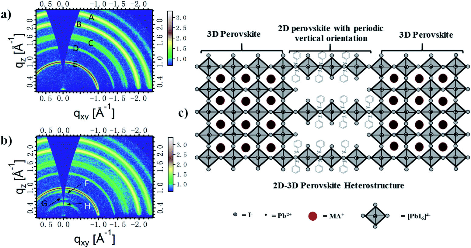 | ||
| Fig. 1 (a and b) GIWAXS images of 3D and anilinium doped 2D/3D perovskite films, respectively, marked with marked diffraction patterns. (c) Schematic representation of 2D–3D perovskite hetero-structure. | ||
The morphology of perovskite films was studied using atomic force microscopy in the tapping mode. The AFM images of 3D and 2D/3D perovskite films are given in Fig. 2a and b, respectively. From the AFM images, it is obvious that the 2D/3D perovskite has a smoother surface and larger grain size as compared to the pristine perovskite film. The addition of anilinium ion in the perovskite precursor solution has given rise to larger grain size. The anilinium ion has conjugated π electrons, which are delocalized through the ring, thus making it a weaker polar base as compared to aliphatic amines. Therefore, in a solution of PbI2, MAI, and AnI, the presence of anilinium ion enhances the solubility of PbI2 in the solution and adduct formation of PbI2 with MAI becomes easier. In this way, the addition of anilinium ion facilitates the formation of crystals with larger grain size and leads to the development of improved perovskite films.41,43
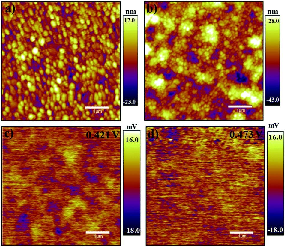 | ||
| Fig. 2 (a and b) Tapping mode AFM images of 3D and 2D/3D perovskites films respectively fabricated on PEDOT:PSS and annealed at 120 °C for 10 minutes. (c) Surface potential of 3D MAPbI3 and (d) 2D/3D [An2PbI4]x[MAPbI3]1−x perovskite films using KPFM. | ||
Similar film morphology is also observed for 2D/3D perovskite loaded with formamidinium and caesium cations (Fig. S2†). The AFM images for FA+ and Cs+ added 2D/3D perovskites are given in Fig. S2.† It was noted that the 2D/3D perovskite containing FA+ and Cs+ ions (total 3 cations; MA+, An+ and FA+, or Cs+ ions in the molar ratio of 0.8:0.15:0.5 respectively in the perovskite precursor solution) display smoother perovskite films with crystal grain size larger than pure 3D MAPbI3 but fractionally less than 2D/3D perovskites without FA+ or Cs+ ions.
The surface potential of MAPbI3 and anilinium doped 2D/3D perovskite was also studied using KPFM to find out the impact of anilinium ion doping. Fig. 2c and d present the surface potential for 3D and 2D/3D perovskites, respectively. [An2PbI4]x[MAPbI3]1−x perovskite has higher surface potential that is 0.52 mV moles higher than that of MAPbI3. Larger crystal grain size of multi-phase perovskite accounts for enhanced surface potential. The comparison of the surface potential figures with respect to their morphology shows that the MPbI3 diagram carries more blue spots, which are an indicator of discontinuity in the surface morphology and this is the reason that it has less surface potential. Fig. 2d presents relatively lesser blue spots and therefore a higher surface potential is measured.39
Another reason for the higher surface potential is the nature of the anilinium ion. Anilinium ion being conjugated and having a cloud of free and polarizable π-electrons is a potential candidate with better electrical properties as compared to the methylammonium ion. This is why the addition of a small amount of anilinium ion has given rise to higher surface potential.30
The UV-Visible absorption and photoluminescence spectra of the fabricated perovskite films are given in Fig. 3. Both 3D MAPbI3 and anilinium doped 2D/3D perovskites have shown similar absorption profile with a broad absorption band over the entire visible region with two significant peaks (Fig. 3a), which are normally observed for such perovskites. The 3D perovskite film was found with characteristic peaks at about 790 nm and 500 nm, and the 2D/3D perovskite with peaks at 784 nm with a slightly lower absorption, which exceeds that of the 3D perovskite in absorption after 494 nm, displaying its second peak at 486 nm. This absorption pattern of the 2D/3D perovskite is in accordance with earlier reports of multidimensional perovskites, where a 2D layered perovskite coexists in a small amount with a bulk of 3D perovskite.39,44,45
 | ||
| Fig. 3 (a) UV-Visible absorption spectra of 3D and 2D/3D perovskite films spin coated onto quartz glass substrates. (b) Photoluminescence spectra of the perovskite films. | ||
The decrease in the absorbance of the 2D/3D perovskite at longer wavelength region is due to the decrease in the quantity of 3D perovskite while the subsequent increase in absorption at lower wavelength corresponds to the presence of a 2D perovskite. The bandgaps of the 3D and 2D/3D perovskites were estimated from Tauc plot (Fig. S3†) and were found to be 1.57 eV and 1.58 eV, respectively. In a broader context, it can be concluded that the addition of a small amount of anilinium iodide with MAI (MAI:AnI = 0.8:0.2) has not caused a significant change in the bandgap and has provided a phase heterojunction with a controlled quantity of 2D phase and a bulk of 3D phase. The addition of FA+ has led to an increase in the absorbance and further decrease in the bandgap while the absorbance spectra of the Cs-doped 2D/3D perovskite just overlaps with the 3D perovskite initially but has shown higher absorbance at lower wavelength corresponding due to the presence of a 2D perovskite component. The absorbance spectra of caesium doped 2D/3D perovskites are given in Fig. S3 of ESI.†
For further authentication and understanding of the improved optoelectronic properties of 2D/3D [An2PbI4]x[MAPbI3]1−x, steady state photoluminescence (PL) was also explored. A broad PL emission peak centred around 780 nm is observed for both 3D and 2D/3D perovskites without any significant change in the PL emission wavelength but it was noted that the 2D/3D perovskite exhibited more luminescence as compared to the 3D MAPbI3 perovskite (Fig. 3b). Usually, the presence of a bulky cation leads to enhanced radiative charge recombination and a rise in the PL emission is observed. Besides, the presence of excess PbI2 in the perovskite film can also have a similar effect and cause higher PL emission.46 This can be correlated to the postulate that the 2D phase is present on a location where the grain boundaries would have been present between the 3D perovskite constituents. Subsequently, the presence of a coherent 2D phase with 3D phase has resulted in upgraded crystallographic linkage between the two phases and reduced crystal defects. Therefore, an increase in the PL intensity is measured.39,45 There are four additional peaks from 820–840 nm. These additional peaks may arise due to some remaining laser pumping or interaction of the laser with the samples.
Photovoltaic device performance
The prepared films were assessed for their photovoltaic performance in inverted structure devices. The planar heterojunction solar cells with ITO/PEDOT:PSS/perovskite/PCBM-61/BCP/Ag architecture was fabricated. The results of photovoltaic performance of the devices are given in Table 1. The current density–voltage (J–V) curves of the champion devices of 3D perovskites and 2D/3D perovskite photovoltaic cells measured under simulated 1 Sun irradiance are given in Fig. 4a and the external quantum efficiency (EQE) spectra are given in Fig. 4b. In terms of PCE, the champion device of anilinium based 2D/3D perovskite based cells yielded 16% photoconversion efficiency while the control 3D perovskite provided a PCE of 13.4%. The devices fabricated with FA+ ion in the 2D/3D perovskite have shown a champion device performance of 13.3% and the device of Cs+ ion doped 2D/3D perovskite film exhibited a PCE of 10.6%. The addition of FAI and CsI in the 2D/3D perovskites shows a decrease in the PCE and other device parameters. The substitution of these ions reduces the amount of 2D component and enhances the quantity of the 3D phase, which leads to reduced device performance.| S. no. | Solution composition, PbI2:MAI:AnI |
V (oc) (V) | J sc (mA cm−2) | FF% | PCE% | Ref. |
|---|---|---|---|---|---|---|
| 1 | 5:4:2 |
0.82 | 10.46 | 69.27 | 5.94 | 29 |
| 2 | 5:4:2 (annealed at 190 °C) |
0.82 | 13.79 | 67.58 | 7.63 | 30 |
| 3 | 1:0.8:0.2 |
1.04 | 25.55 | 60.00 | 15.96 | This work |
| 4 | 1:08:0.15, with FAI 0.05 molar ratio |
0.90 | 28.16 | 52.12 | 13.25 | This work |
| 5 | 1:08:0.15, with CsI 0.05 molar ratio |
0.90 | 19.91 | 60.51 | 10.73 | This work |
| 6 | 1:1:0 |
1.03 | 23.09 | 56.15 | 13.38 | This work |
 | ||
| Fig. 4 (a) J–V curve of 3D and 2D/3D perovskite champion devices with a cell structure diagram in the inset. (b) EQE spectra of 3D MAPbI3 and 2D/3D [AnPbI4]x[MAPbI3](1−x) perovskite devices. | ||
Comparing the EQE spectra of 3D and 2D/3D perovskites, (Fig. 4b) a shift in the EQE spectra of the 2D/3D perovskite at about 500 nm indicated the presence of a 2D layered perovskite component, which caused enhanced excitonic absorption around this wavelength.31 The EQE spectra matches well with the absorbance spectra but the integrated Jsc value is lower as compared to Jsc measured under 1 sun irradiation. (Integrated Jsc value and resulting PCE are given in Table S1.†) This is because when Jsc is measured from the solar simulator, cell operates under maximum power point, while during the EQE measurement, cell operation takes place at a point lower than the maximum power point.47
The higher value of Jsc for 2D/3D perovskites indicates that presence of a small quantity of anilinium based 2D layered perovskite with vertical orientation does not hinder photocurrent extraction. Rather, it improves the photo-current generation due to presence of a conjugated cation, which also leads to enhanced PL emission.30,37 The coexistence of the two phases in a combined perovskite hetero-structure has also saved the loss of charge carries at the grain boundaries because there is a high potential barrier between the holes at the junction of two phases. This may be regarded as a reason for heightened PL emission and better optoelectronic performance of the devices with 2D/3D perovskite.48
It is evident from these results that the 2D/3D perovskite has performed better than the 3D perovskite MAPbI3 in the same cell architecture. This improvement in the photovoltaic performance can be attributed to better electronic transport properties as indicated by the higher value of short circuit current density, without affecting the radiative charge recombination along with improved film morphology with larger crystal grain size and increased surface potential. All these factors contributed to the better performance of anilinium based 2D/3D perovskite over the 3D perovskite.
The results of this study were also compared with the previous reports of anilinium based 2D/3D perovskite with a lower n value (n = 1 to 5). In the previous studies, different molar ratios of PbI2, MAI, and AnI were used. For n = 5 for the 2D/3D perovskite, the molar ratio used was 5:4:2, respectively.29,30 We have instead optimized a different ratio of PbI2, MAI, and AnI, which has proficiently worked as a better composition for perovskite precursor solutions and provided a unique 2D/3D perovskite of its own kind that resulted in a 2 fold increase in the PCE of anilinium based 2D/3D perovskites (detail of all the tried compositions and their photovoltaic performance is given in Table S2, in ESI†) and a new structural strategy with a proven potential for even better results in future was explored.
We have also compared the photovoltaic performance of these 2D/3D perovskites with previously reported 2D/3D perovskites of similar kind, where a phase pure 2D perovskite (n = 1) co-exists with a 3D perovskite. The results are summarized in Table S3 in the ESI.† Based on these results and as per the best of our knowledge, we have reported a perovskite solar device of the highest efficiency based on the ITO/PEDOT:PSS/perovskite/PCBM/BCP/Ag cell architecture.37,38,44,49–51 Moreover, this paper also reports the highest efficiency of a 2D/3D perovskite utilizing anilinium ion as a larger cation.
Additionally, we remeasured the PCE of the devices after keeping them placed open in the laboratory environment with normal humidity for 18 days. It was found that the 2D/3D perovskite maintained its photovoltaic performance with the same parameters without any variation while pristine 3D MAPbI3 has lost 45% of its initial PCE.
3. Conclusion
In conclusion, we report a highly efficient anilinium based 2D/3D perovskite material, in which 2D layered perovskite An2PbI4 with a periodic vertical orientation is coexisting with a bulk of 3D MAPbI3. In this multidimensional perovskite, the ratio of 3D to 2D perovskite is 8:1, which is crucial for its high optoelectronic properties. This dimensional engineering of the 2D/3D perovskite has improved all the parameters of 3D MAPbI3 without any considerable alteration in its band gap value. The 2D/3D perovskite [An2PbI4]x[MAPbI3](x−1) has outperformed the 3D perovskite in all limits such as film morphology and crystal grain size, PL emission, EQE, surface potential, and in all solar cell parameters.
This coexistence of the 2D phase with the 3D phase has radiative charge recombination, which is a reason for its improved photoconversion performance, and it has given rise to the higher value of Jsc. Moreover, anilinium ion has free and polarizable π-electrons; this structural quality has provided a better choice for a larger cation in multidimensional perovskites. In future, this cation needs more attention of the researchers to obtain even better results.
Author contributions
MSA and RA conceived the idea. MSA and BW performed device fabrication and characterization. SH and MSA completed AFM and KPFM analysis. JZ and MSA conducted GIWAXS experiments. Z Wang, CY, and MSA carried out EQE, UV-Visible, and PL analysis. All the authors contributed in data analysis and results interpretation. MSA, RA, and Z. Wei wrote the manuscript. RA and Z. Wei guided the whole research project.Conflicts of interest
“There are no conflicts to declare”.Acknowledgements
We are thankful to the Higher Education Commission (HEC) of Pakistan, for providing IRSIP fellowship.Notes and references
- H. S. Kim, C. R. Lee, J. H. Im, K. B. Lee, T. Moehl, A. Marchioro, S. J. Moon, R. H. Baker, J. H. Yum, J. E. Moser, M. Grätzel and N. G. Park, Sci. Rep., 2012, 2, 591 CrossRef PubMed.
- http://www.nrel.gov/ncpv/images/efficiency_chart.jpg .
- J. Burschka, N. Pellet, S. J. Moon, R. Humphry-Baker, P. Gao, M. K. Nazeeruddin and M. Grätzel, Nature, 2013, 499, 316 CrossRef CAS PubMed.
- M. Liu, M. B. Johnston and H. J. Snaith, Nature, 2013, 501, 395 CrossRef CAS PubMed.
- A. F. Wells, Structural Inorganic Chemistry, Clarendon Press, Oxford, 1984 Search PubMed.
- A. J. Pearson, G. E. Eperon and P. E. Hopkinsin, Adv. Energy Mater., 2016, 6, 1600014 CrossRef.
- G. E. Eperon, S. D. Stranks, C. Menelaou, M. B. Johnston, L. M. Herz and H. J. Snaith, Energy Environ. Sci., 2014, 7, 982 RSC.
- N. Aristidou, I. S. Molina, T. Chotchuangchutchaval, M. Brown, L. Martinez, T. Rath and S. A. Haque, Angew. Chem., Int. Ed., 2015, 54, 8208 CrossRef CAS PubMed.
- A. Krishna, S. Gottis, M. K. Nazeeruddin and F. Sauvage, Adv. Funct. Mater., 2018, 29, 1806482 CrossRef.
- Z. Wang, D. P. McMeekin, N. Sakai, S. van Reenen, K. Wojciechowski, J. B. Patel, M. B. Johnston and H. J. Snaith, Adv. Mater., 2016, 29, 1604186 CrossRef PubMed.
- G. Niu, X. Guo and L. Wang, J. Mater. Chem. A, 2015, 3, 8970 RSC.
- A. M. A. Leguy, Y. Hu, M. C. Quiles, M. I. Alonso, O. J. Weber, P. Azarhoosh, M. van Schilfgaarde, M. T. Weller, T. Bein, J. Nelson, P. Docampo and P. R. F. Barnes, Chem. Mater., 2015, 27, 3397 CrossRef CAS.
- J. A. Christians, P. A. Miranda Herrera and P. V. Kamat, J. Am. Chem. Soc., 2015, 137, 1530 CrossRef CAS PubMed.
- J. S. Manser, M. I. Saidaminov, J. A. Christians, O. M. Bakr and P. V. Kamat, Acc. Chem. Res., 2016, 49, 330 CrossRef CAS PubMed.
- J. Yang, B. D. Siempelkamp, D. Liu and T. L. Kelly, ACS Nano, 2015, 9, 1955 CrossRef CAS PubMed.
- D. A. Egger, L. Kronik and A. M. Rappe, Angew. Chem., Int. Ed., 2015, 54, 12437 CrossRef CAS PubMed.
- G. Niu, W. Li, F. Meng, L. Wang, H. Dong and Y. Qiu, J. Mater. Chem. A, 2014, 2, 705 RSC.
- C. Yi, J. Lou, S. Meloni, A. Boziki, N. A. Astani, C. Gratzel, S. M. Zakeeruddin, U. Rothlisberger and M. Gratzel, Energy Environ. Sci., 2016, 9, 656 RSC.
- D. P. McMeekin, G. Sadoughi, W. Rehman, G. E. Eperon, M. Saliba, M. T. Horantner, A. Haghighirad, N. Sakai, L. Korte, M. B. Johnston, L. M. Herz and H. J. Snaith, Science, 2016, 351, 151 CrossRef CAS PubMed.
- S. N. Ruddlesen and P. Popper, Acta Crystallogr., 1957, 10, 538 CrossRef.
- S. N. Ruddlesen and P. Popper, Acta Crystallogr., 1958, 101, 54 CrossRef.
- Y. Chen, Y. Sun, J. Peng, J. Tang, K. Zheng and Z. Liang, Adv. Mater., 2018, 30, 1703487 CrossRef PubMed.
- I. C. Smith, E. T. Hoke, D. Solis-Ibarra, M. D. McGehee and H. I. Karunadasa, Angew. Chem., 2014, 126, 11414 CrossRef.
- R. K. Misra, B. Cohen, L. Iagher and L. Etgar, ChemSusChem, 2017, 10, 3712 CrossRef CAS PubMed.
- L. N. Quan, M. Yuan, R. Comin, O. Voznyy, E. M. Beaureguard, S. Hoogland, A. Buin, A. R. Kirmani, K. Zhao, A. Amassian, D. H. Kim and E. H. Sargent, J. Am. Chem. Soc., 2016, 138, 2649 CrossRef CAS PubMed.
- L. N. Quan, Y. Zhao, F. P. G. de Arquer, R. Sabatini, G. Walters, O. Voznyy, R. Comin, Y. Li, J. Z. Fan, H. Tan, J. Pan, M. Yuan, O. M. Bakr, Z. Lou, D. H. Kim and E. H. Sargent, Nano Lett., 2017, 7, 976 Search PubMed.
- N. Li, Z. Zhu, C. Chueh, H. Liu, B. Peng, A. Petrone, X. Li, L. Wamg and A. K. Y. Jen, Adv. Energy Mater., 2017, 7, 1601307 CrossRef.
- H. Tsai, W. Nie, J.-C. Blancon, C. C. Stoumpos, R. Asadpour, B. Harutyunyan, A. J. Neukirch, R. Verduzco, J. J. Crochet, S. Tretiak, L. Pedesseau, J. Even, M. A. Alam, G. Gupta, J. Lou, P. M. Ajayan, M. J. Bedzyk, M. G. Kanatzidis and A. D. Mohite, Nature, 2016, 536, 312 CrossRef CAS PubMed.
- J. Rodríguez-Romero, B. C. Hames, I. n. Mora-Seró and E. M. Barea, ACS Energy Lett., 2017, 2, 1969 CrossRef.
- J. Rodríguez-Romero, B. C. Hames, P. Galar, A. Fakharuddin, I. Suarez, L. Schmidt-Mende, J. P. Martínez-Pastor, A. Douhal, I. Mora-Seró and E. M. Barea, Phys. Chem. Chem. Phys., 2018, 20, 30189 RSC.
- Y. Zhang, S. Li, W. Yang, M. K. Joshi and X. Fang, J. Phys. Chem. Lett., 2019, 10, 2400 CrossRef CAS PubMed.
- Y. Zhang, W. Xu, X. Xu, J. Cai, W. Yang and X. Fang, J. Phys. Chem. Lett., 2019, 10, 836 CrossRef CAS PubMed.
- C. Lin, B. Cheng, T. Li, J. R. D. Retamal, T. Wei, H. Fu, X. Fang and J. He, ACS Nano, 2019, 13, 1168 CAS.
- A. M. Alamri, B. Chen and J. He, IEEE Trans. Nanotechnol., 2018, 19, 1 Search PubMed.
- A. M. Alamri, S. Leung, M. Vaseem, A. Shamim and J. He, IEEE Trans. Electron Devices, 2019, 66, 2657 CAS.
- W. Yang, J. Chen, Y. Zhang, Y. Zhang, J. He and X. Fang, Adv. Funct. Mater., 2019, 29, 1808182 CrossRef.
- Z. Chen, M. Liu, Z. Li, T. Shi, Y. Yang, H. Yip and Y. Cao, iScience, 2018, 9, 337 CrossRef CAS PubMed.
- F. Wang, X. Jiang, H. Chen, Y. Shang, H. Liu, J. Wei, W. Zhou, H. He, W. Liu and Z. Ning, Joule, 2018, 2, 1 CrossRef.
- M. Li, H. Yeh, Y. Chiang, U. Jeng, C. Su, H. Shiu, Y. Hsu, N. Kosugi, T. Ohigashi, Y. Chen, P. Shen, P. Chen and T. Guo, Adv. Mater., 2018, 30, 1801401 CrossRef PubMed.
- K. M. Fransishyn, S. Kundu and T. L. Kelly, ACS Energy Lett., 2018, 3, 2127 CrossRef CAS.
- B. Park, N. Kedem, M. Kulbak, D. Y. Lee, W. S. Yang, N. J. Jeon, J. Seo, G. Kim, K. J. Kim, T. J. Shin, G. Hodes, D. Cahen and S. I. Seok, Nat. Commun., 2018, 9, 3301 CrossRef PubMed.
- W. S. Yang, B. Park, E. H. Jung, N. J. Jeon, Y. C. Kim, D. U. Lee, S. S. Shin, J. Seo, E. K. Kim, J. H. Noh and S. I. Seok, Science, 2017, 359, 1376 CrossRef PubMed.
- S. Mabrouk, B. Bahrami, A. Gurung, K. M. Reza, N. Adhikari, A. Dubey, R. Patekh, S. Yang and Q. Qiao, Sustainable Energy Fuels, 2017, 1, 2162 RSC.
- G. Grancini, C. Roldan-Carmona, I. Zimmermann, E. Mosconi, X. Lee, D. Martineau, S. Narbey, F. Oswald, F. D. Angelis, M. Gratzel and M. K. Nazeeruddin, Nat. Commun., 2017, 9, 3301 Search PubMed.
- Z. Wang, Q. Lin, F. P. Chmeil, N. Sakai, L. M. Herz and H. J. Snaith, Nat. Energy, 2017, 2, 17135 CrossRef CAS.
- Q. Chen, H. Zhou, T. Song, S. Luo, Z. Hong, H. Duan, L. Dou, Y. Liu and Y. Yang, Nano Lett., 2014, 14, 4158 CrossRef CAS PubMed.
- L. Iagher and L. Etgar, ACS Energy Lett., 2018, 3, 366 CrossRef CAS.
- J. Lee, Z. Dai, T. Han, C. Choi, S. Chang, S. Lee, N. D. Marco, H. Zhao, P. Sun, Y. Huang and Y. Yang, Nat. Commun., 2018, 9, 3021 CrossRef PubMed.
- K. Yao, X. Wang, Y. Xu and F. Li, Nano Energy, 2015, 18, 165 CrossRef CAS.
- K. Yao, X. Wang, F. Li and L. Zhou, Chem. Commun., 2015, 51, 15430 RSC.
- J. Chen, D. Lee and N. G. Park, ACS Appl. Mater. Interfaces, 2017, 9, 36338 CrossRef CAS PubMed.
Footnote |
| † Electronic supplementary information (ESI) available. See DOI: 10.1039/c9se00817a |
| This journal is © The Royal Society of Chemistry 2020 |