
 Open Access Article
 This Open Access Article is licensed under a
 Creative Commons Attribution 3.0 Unported Licence
Simultaneous manifestation of metallic conductivity and single-molecule magnetism in a layered molecule-based compound†
Yongbing
Shen
 *a,
Hiroshi
Ito
*b,
Haitao
Zhang
c,
Hideki
Yamochi
de,
Seiu
Katagiri
b,
Shinji K.
Yoshina
b,
Akihiro
Otsuka
de,
Manabu
Ishikawa
d,
Goulven
Cosquer
f,
Kaiji
Uchida
a,
Carmen
Herrmann
c,
Takefumi
Yoshida
a,
Brian K.
Breedlove
a and
Masahiro
Yamashita
*ag
*a,
Hiroshi
Ito
*b,
Haitao
Zhang
c,
Hideki
Yamochi
de,
Seiu
Katagiri
b,
Shinji K.
Yoshina
b,
Akihiro
Otsuka
de,
Manabu
Ishikawa
d,
Goulven
Cosquer
f,
Kaiji
Uchida
a,
Carmen
Herrmann
c,
Takefumi
Yoshida
a,
Brian K.
Breedlove
a and
Masahiro
Yamashita
*ag
aDepartment of Chemistry, Graduate School of Science, Tohoku University, Sendai, Japan. E-mail: shenyongbing17@gmail.com
bDepartment of Applied Physics, Nagoya University, Chikusa-ku, Nagoya 464-603, Japan
cInstitute of Inorganic and Applied Chemistry, University of Hamburg, Martin-Luther-King-Platz 6, 20146 Hamburg, Germany
dDivision of Chemistry, Graduate School of Science, Kyoto University, Sakyo-ku, Kyoto 606-8502, Japan
eResearch Center for Low Temperature and Materials Sciences, Kyoto University, Sakyo-ku, Kyoto 606-8501, Japan
fResearch Group of Solid Material Chemistry, Graduate School of Science, Hiroshima University, 1-3-1 Kagamiyama, Higashihiroshima, Hiroshima, 739-8526, Japan
gSchool of Materials Science and Engineering, Nankai University, Tianjin 300350, China
First published on 1st September 2020
Abstract
Single-molecule magnets (SMMs) show superparamagnetic behaviour below blocking temperature at the molecular scale, so they exhibit large magnetic density compared to the conventional magnets. Combining SMMs and molecular conductors in one compound will bring about new physical phenomena, however, the synergetic effects between them still remain unexplored. Here we present a layered molecule-based compound, β′′-(BEDO-TTF)4 [Co(pdms)2]·3H2O (BO4), (BEDO-TTF (BO) and H2pdms are bis(ethylenedioxy)tetrathiafulvalene and 1,2-bis(methanesulfonamido)benzene, respectively), which was synthesized by using an electrochemical approach and studied by using crystal X-ray diffraction. This compound simultaneously exhibited metallic conductivity and SMM behaviour up to 11 K for the first time. The highest electrical conductivity was 400–650 S cm−1 at 6.5 K, which is the highest among those reported so far for conducting SMM materials. Furthermore, antiferromagnetic ordering occurred below 6.5 K, along with a decrease in conductivity, and the angle-independent negative magnetoresistance suggested an effective electron correlation between the conducting BO and Co(pdms)2 SMM layers (d–π interactions). The strong magnetic anisotropy and two-dimensional conducting plane play key roles in the low-temperature antiferromagnetic semiconducting state. BO4 is the first compound exhibiting antiferromagnetic ordering among SMMs mediated by π-electrons, demonstrating the synergetic effects between SMMs and molecular conductors.
Introduction
Exploitation of multifunctionalities on the nanoscale is a critical challenge in modern chemistry to satisfy the rapidly growing demands in electronics.1 Combining both electrical conductivity (σ) and magnetism in one compound to afford bifunctional materials has been intensively studied by P. Day and H. Kobayashi et al.2 The discovery of the giant magnetoresistance (GMR) effect by A. Fert et al.3 and P. Grünberg et al.4 in 1988 established the area of spintronics and significantly improved the size and storage capacity of magnetic digital data drives in the 21st century. The research in this field has concentrated on combining molecular conductors, such as bis(ethylenedithio)tetrathiafulvalene (BEDT-TTF),5 7,7,8,8-tetracyanoquinodimethane (TCNQ)6 and various single-molecule magnets (SMMs), such as [Mn2III(5-MeOsaltmen)2]− and [Dy(CF3COO)4]−,5,7 where 5-MeOsaltmen is the N,N′-(1,1,2,2-tetramethylethylene)-bis(5-methoxysalicylideneiminato) dianion. SMMs can magnetically store information at a molecular level.8,9 Thus, they are good candidates for use in molecular spintronic devices, like spin-valves, and due to their long relaxation times, they are applied in quantum computers.10 Moreover, the combination of SMMs and electrical conductors may allow for nanoscale functionality beyond Moore's limitation.11The construction of conducting SMMs has been examined;12 however, so far obtained materials exhibited semiconductor behaviour and SMM behaviour in different temperature ranges. They conduct above liquid nitrogen temperature and behave as SMMs at liquid helium temperature, and no synergism has been observed. Therefore, the search for suitable molecular conductors and SMMs has been intensively pursued. Recently, our group has reported (TTF)2[Co(pdms)2], which behaves as a semiconductor and an SMM in the same temperature region.13 Due to its unusual mixed stacking structure, strong charge transfer between TTF and [Co(pdms)2] affords electrical conduction down to 2 K with SMM properties up to 5 K, however, it is not metallic.
The oxygen analogue of BEDT-TTF (ET) is BEDO-TTF (BO) (Fig. 1a), which is a well-known donor molecule to give metallic and superconducting ion radical salts.14 The difference between the two molecules lies in the fact that, in BO, the four sulfur atoms in the six-member rings of ET are substituted by smaller and lighter oxygen atoms in BO, which can effectively shorten the intermolecular S⋯S distance between the central TTFs. In crystals of metallic BO complexes, donor molecules aggregate into layered structures, forming uniform (such as I3-type) arrays connected by intrastack C–H⋯O hydrogen bonds and side-by-side heteroatom short contacts to form a stable 2D metal.15 Following this idea, (BEDO-TTF)4(ReF6)·3H2O was the first example of the application of BO molecules to preserve relatively high σ down to low temperature (σ4.2 K = 47 S cm−1) for which the field-induced slow relaxation of magnetization was observed below 4 K, but no synergetic effects were reported.16 On the other hand, we selected a four-coordinate Co-based SMM, [Co(pdms)2]2− (Fig. 1b). [Co(pdms)2]2− is an outstanding SMM with a large negative zero-field splitting D value (D = −115 cm−1),13 which is necessary for high energy barrier SMMs. The low energy absorbance band at 1200 nm (calculated at 960 nm by the TD-CAM-B3LYP method) corresponds to the electron transition from the 4B1 orbital to the 4E orbital of the cobalt ion (Fig. S1†), indicating that the strong ligand field of the bis(sulfonamido) ligand in combination with a strong axial distortion accounts for the large D value. The first semiconducting SMM with σ300 K = 0.22 S cm−1 was reported by H. Hiraga et al.7a in 2007 and further explored by several groups in the following decade (Fig. 1c); the highest σ was reported to be 47 S cm−1 at 4.2 K by N. D. Kushch et al. in 2018,16a but their SMMs were not metals. Here we report the first metallic conducting SMM material, β′′-(BO)4[Co(pdms)2]·3H2O, which has the highest σ value (400–650 S cm−1 at 6.5 K by measuring six single-crystals) in the family of conducting SMM materials and exhibits SMM behaviour in the antiferromagnetic phase with a TB up to 11 K. The synergetic effect, which is expected from the band structure calculation, has been found as the antiferromagnetic interactions and magnetoresistance (MR) at low temperatures.
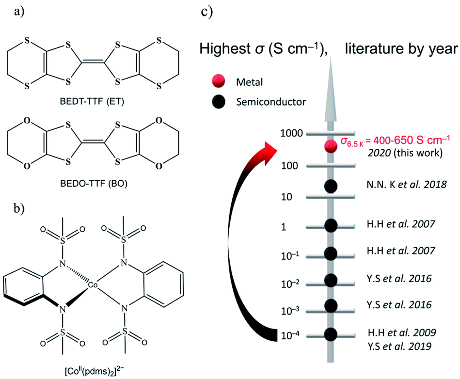 | ||
| Fig. 1 Organic conductors and single-molecule magnets. (a) Structural diagrams of BEDT-TTF (ET) and BEDO-TTF (BO). (b) Tetrahedrally coordinated structure of [Co(pdms)2]2−. (c) The evolution of the highest σ by year for the reported conducting SMM materials: black and red dots represent semiconductors and metals, respectively. The original literature abbreviated in this panel is listed in ref. 12. | ||
Results and discussion
Crystal structure
BO4 (CCDC: 1970380†) crystallized in the centrosymmetric triclinic P![[1 with combining macron]](https://www.rsc.org/images/entities/char_0031_0304.gif) space group with four crystallographically independent BO molecules, one Co(pdms)2 unit and three water molecules (Fig. 2a) with unit cell dimensions a = 12.498(1) Å, b = 13.717(1) Å, c = 22.91(2) Å, α = 102.965(12)°, β = 101.501(14)° and γ = 99.116(18)° at 120 K. The total positive charge of the four BO molecules is compensated by [Co(pdms)2]2− to give the charge neutrality of (BO)4[Co(pdms)2]·3H2O. Fig. 2b shows the packing structure in the bc plane. The SMM layer alternates with the metallic layer along the c-axis. The thicknesses of the layers are 7.2 Å and 11.0 Å, respectively, indicating that both of them are 2D nanosheets. Numbers of hydrogen-bonds (C–H⋯O) are observed between BO and SMM layers in addition to those within the BO layer, both of which stabilize the crystal structure (Fig. S4a and Table S2†). As shown in Fig. 2c, the Co ions are arranged to form an infinite arrangement of parallelograms in the ab plane, where the shortest distance between two Co ions is 8.6 Å, and the angle (φ) between three Co ions in one parallelogram is 42°. The magnetic easy axes of all Co(pdms)2 units are aligned along the b-axis to show a strong one-dimensional (1D) magnetic anisotropy (Fig. S5†). Fig. 2d shows the packing of the BO molecules in I3-type arrangement (corresponding to β′-type for ET salts17). While the intermolecular S⋯S and S⋯O atomic contacts shorter than the sum of van-der-Waals radii are observed along the a-axis (between side-by-side BO pairs) and along the a–b direction, significant magnitudes of intermolecular orbital overlap (transfer integral) are manifested along the a-axis and along the 3a + 2b direction (Fig. S4b†).
space group with four crystallographically independent BO molecules, one Co(pdms)2 unit and three water molecules (Fig. 2a) with unit cell dimensions a = 12.498(1) Å, b = 13.717(1) Å, c = 22.91(2) Å, α = 102.965(12)°, β = 101.501(14)° and γ = 99.116(18)° at 120 K. The total positive charge of the four BO molecules is compensated by [Co(pdms)2]2− to give the charge neutrality of (BO)4[Co(pdms)2]·3H2O. Fig. 2b shows the packing structure in the bc plane. The SMM layer alternates with the metallic layer along the c-axis. The thicknesses of the layers are 7.2 Å and 11.0 Å, respectively, indicating that both of them are 2D nanosheets. Numbers of hydrogen-bonds (C–H⋯O) are observed between BO and SMM layers in addition to those within the BO layer, both of which stabilize the crystal structure (Fig. S4a and Table S2†). As shown in Fig. 2c, the Co ions are arranged to form an infinite arrangement of parallelograms in the ab plane, where the shortest distance between two Co ions is 8.6 Å, and the angle (φ) between three Co ions in one parallelogram is 42°. The magnetic easy axes of all Co(pdms)2 units are aligned along the b-axis to show a strong one-dimensional (1D) magnetic anisotropy (Fig. S5†). Fig. 2d shows the packing of the BO molecules in I3-type arrangement (corresponding to β′-type for ET salts17). While the intermolecular S⋯S and S⋯O atomic contacts shorter than the sum of van-der-Waals radii are observed along the a-axis (between side-by-side BO pairs) and along the a–b direction, significant magnitudes of intermolecular orbital overlap (transfer integral) are manifested along the a-axis and along the 3a + 2b direction (Fig. S4b†).
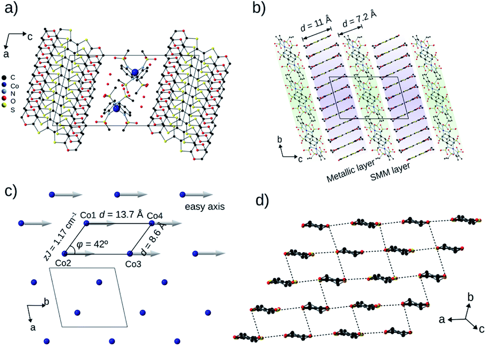 | ||
| Fig. 2 Crystal structure of BO4 at 120 K. (a) A unit cell projected along the b-axis (black: C, blue: Co, pale blue: N, red: O and yellow: S). (b) Packing structure in the bc plane. The SMM layer (green background) alternates with the conducting layer (violet background) via short contacts, and the thicknesses of the SMM and conducting layers are 7.2 Å and 11.0 Å, respectively. (c) The arrangement of the Co ions in the SMM layer in the ab plane. The arrows represent the direction of the easy axis of the Co ions in the Co(pdms)2 molecules. The angle (φ) between three Co ions in one parallelogram is 42°, and the distances between two adjacent Co ions are 8.6 Å and 13.7 Å. (d) The BO molecules arranged side-by-side along the a-axis and face-to-face in the a–b direction. The black dotted lines represent the short contacts (S⋯S and S⋯O) between BO molecules along the a-axis and a–b direction. All hydrogen atoms are omitted for clarity. | ||
Spectroscopic properties
In solid-state UV-Vis-NIR absorption spectra of BO4, several broad bands were observed at room temperature (Fig. S6a†). The lowest energy broad absorption extending to the near IR region (<7500 cm−1) corresponds to the intermolecular charge-transfer (CT) transition between partially oxidized BO molecules. The absorption band at around 12![[thin space (1/6-em)]](https://www.rsc.org/images/entities/char_2009.gif) 000 cm−1 was assigned to the electronic transition within a BO radical cation (electronic transition from the second HOMO to HOMO).15b In EPR spectra, a single peak with g = 2.004 was observed at room temperature (Fig. S6b†), confirming the presence of a BO radical. To further investigate the electronic structures, infrared reflectance spectroscopy was carried out on single crystals. Fig. S6c† shows room temperature reflectance spectra with the incident light polarized parallel to the ab plane. This reflectance spectrum was well fitted by a Drude–Lorentz model in the range of 550–7800 cm−1: plasma frequency (ωρ), relaxation rate (Γ) and dielectric constant (ε∞) are evaluated as 6331.3 cm−1, 3394.2 cm−1, and 3.48, respectively. The reflectance spectrum indicates a highly conducting nature.18 Raman spectroscopy was carried out to determine the charge on the BO molecules to understand the degree of CT in the BO layer. The room-temperature Raman band at around 1480 cm−1 observed to be a superposition of two bands (∼1477 cm−1 and ∼1483 cm−1) was attributed to the totally symmetric C
000 cm−1 was assigned to the electronic transition within a BO radical cation (electronic transition from the second HOMO to HOMO).15b In EPR spectra, a single peak with g = 2.004 was observed at room temperature (Fig. S6b†), confirming the presence of a BO radical. To further investigate the electronic structures, infrared reflectance spectroscopy was carried out on single crystals. Fig. S6c† shows room temperature reflectance spectra with the incident light polarized parallel to the ab plane. This reflectance spectrum was well fitted by a Drude–Lorentz model in the range of 550–7800 cm−1: plasma frequency (ωρ), relaxation rate (Γ) and dielectric constant (ε∞) are evaluated as 6331.3 cm−1, 3394.2 cm−1, and 3.48, respectively. The reflectance spectrum indicates a highly conducting nature.18 Raman spectroscopy was carried out to determine the charge on the BO molecules to understand the degree of CT in the BO layer. The room-temperature Raman band at around 1480 cm−1 observed to be a superposition of two bands (∼1477 cm−1 and ∼1483 cm−1) was attributed to the totally symmetric C![[double bond, length as m-dash]](https://www.rsc.org/images/entities/char_e001.gif) C vibration of the BO (v3(Ag) mode, Fig. S6d†). The position of the v3(Ag) mode depends on the charge on BO and can be used to determine the charge density (ρ) using the following equation: ρ = (1524.9 − ν3(obs) (cm−1))/109.0.19 The possibility of inhomogeneous charges on BO molecules is thus supposed; the calculated charges are +0.44 and +0.38, respectively.
C vibration of the BO (v3(Ag) mode, Fig. S6d†). The position of the v3(Ag) mode depends on the charge on BO and can be used to determine the charge density (ρ) using the following equation: ρ = (1524.9 − ν3(obs) (cm−1))/109.0.19 The possibility of inhomogeneous charges on BO molecules is thus supposed; the calculated charges are +0.44 and +0.38, respectively.
Magnetic properties
Fig. 3a shows the static magnetic susceptibility temperature products, χT of BO4, as a function of temperature in a 0.1 T field measured in zero field cooling (ZFC) and field cooling (FC) modes. The observed χT value of 3.22 cm3 K mol−1 at 300 K is 0.08 cm3 K mol−1 larger than the value expected for an S = 3/2 ion with g = 2.59 in (HNEt3)2[Co(pdms)2],20 which indicates that most of the paramagnetic susceptibility comes from Co(pdms)2. Hence, the contribution from the BO layer is estimated only to be around 2.7 × 10⁻⁴ cm3 mol−1, which is consistent with the metallic nature of the conducting layer. This χ value agrees well with the χ–T plot of (BO)4[Zn(pdms)2]·3H2O showing almost temperature-independent χ with the value of 2.8 × 10⁻⁴ cm3 mol−1 (Fig. S7†), which is comparable to χ at room temperature for ET based metallic salts.21 On cooling BO4, the χT value gradually decreased to 2.25 cm3 K mol−1 at 40 K due to the depopulation of Co ions. For T > 40 K, the Curie (C) and Weiss constants (θ) were estimated to be 1.93 cm3 K mol−1 and +10.2 K by using the Curie–Weiss law. Thus, the indirect ferromagnetic interactions below 10.2 K between Co ions mediated by the pdms ligand were assigned. A. A. Fraerman et al. have reported that the region with ferromagnetic long-range interaction of a magnetic dipole system in an orthorhombic lattice is stable.22 It has been shown that the ground state of the system depends on the rhombic angle (φ). If φ < 60°, the dipoles are ordered ferromagnetically and the φ value of 42° observed for BO4 is regarded to be adequate to manifest ferromagnetic interactions in a parallelogram lattice (note, however, that the detailed mechanism behind magnetic interactions in this system is not obvious, and that direct magnetic–dipole interactions are expected to be weak here). After rising again, χT abruptly decreased upon cooling below 6.5 K to 2.68 and 2.33 cm3 K mol−1 in ZFC and FC modes, respectively, indicating that there are antiferromagnetic interactions. To model the static magnetic properties, the spin Hamiltonian , where Si = SCo = 3/2 and where DCo stands for the zero-field splitting parameter for a CoII ion, was employed. Parameters of g(Co) = 2.19, DCo = −67.3 cm−1, and zJ = 1.05 cm−1 under FC conditions and g(Co) = 2.10, DCo = −59.0 cm−1, and zJ = 1.17 cm−1 under ZFC conditions were obtained from fitting (eqn S1†). The small zJ values indicate that there are weak magnetic interactions between the Co(pdms)2 units in the SMM layer (Fig. 2c). The Néel temperature (TN), defined as peaks of the ln(χT)–T−1 plot, slightly shifted from 7.0 to 11 K when the magnetic field was increased from 200 to 10000 Oe (Fig. S8†), indicating that there is antiferromagnetic ordering. The χ and χT values were investigated in fields of 10–1000 Oe below 20 K in ZFC and FC modes (Fig. S8†). The clear divergences of the χ and χT values in ZFC and FC modes when T < 11 K are direct evidence for blocking temperature (TB) of SMMs up to 11 K and TN up to 6.5 K. To the best of our knowledge, this is the highest TB among those reported for four-coordinate Co2+ based SMMs. Fig. 3b shows the field dependence of the magnetization (M–H curve) in the initial field sweep and the dM/dH curve measured at 2.5 K. A stepwise increase was observed, indicating the presence of the spin–flop transition in the field of H1 and H2 (H2 > H1). The spin–flop transitions were observed in an H1 of 430 Oe and an H2 of 4700 Oe at 2.5 K and an H1 of 480 Oe at 5 K (Fig. S9†), indicating a phase transition from an antiferromagnetic ground state to a paramagnetic ground state, consistent with the observation of a Néel peak in the χ–T plots in weak fields (Fig. S8†), and the resultant magnetic moments may come from the spin canting between localized Co spins and delocalized π spins. The spin–flop transition showed that the antiferromagnetic interactions were suppressed in an applied field of H1. H1 corresponds to the interactions between the SMM layers, which cause the second relaxation process observed in the alternating current (ac) magnetic susceptibility measurements (describe below). Therefore, the strength of antiferromagnetic interactions (zJ′) was calculated to be 0.0074 cm−1 by using a mean-field approximation model, 2|zJ′|ST2 = gSTμBH1 with ST = 3 and g = 2.0, where an ST of 3 was the largest magnetic moment (two ferromagnetic Co(pdms)2 units) in the SMM layer. H2 could be assigned to the coupling between the SMM and BO layers. Magnetic hysteresis loops were observed up to 5 K with a remnant magnetization of 0.08 Nβ and a coherence field of 23 Oe at 2.5 K, indicating that BO4 shows SMM behaviour (Fig. S10†).
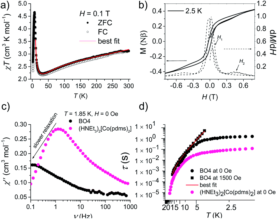 | ||
| Fig. 3 Magnetic properties. (a) Temperature dependence χT (black circles) in a 0.1 T field in field cooling (FC) and zero field cooling (ZFC) modes, respectively. The solid red lines represent the best fit using anisotropic spins. (b) Magnetic hysteresis of the magnetization at a sweep rate of 200 Oe·s−1 at 2.5 K and the first differential curve of dM/dH (dashed curves) in the range of −0.8 to +0.8 T. (c) A comparison of frequency dependences of out-of-phase ac magnetic susceptibilities χ′′ of BO4 and (HNEt3)2[Co(pdms)2] in a field of 0 Oe. (d) τ as a function of T in fields of 0 and 1500 Oe for BO4 and (HNEt3)2[Co(pdms)2]. The black circles, pink circles and the red curve represent the experimental data and best fit, respectively. | ||
Fig. 3c and S11† show the frequency dependence of the in-phase (χ′) and out-of-phase (χ′′) ac magnetic susceptibility, χ′′, at 0 Oe at various temperatures. Dual relaxation peaks in the range of 0.1–1000 Hz, with the first relaxation process at low frequency and the second relaxation process at high frequency. The first relaxation process corresponds to the reversal of the spins of the Co ions, and the second relaxation process is related to the antiferromagnetic interactions between two adjacent SMM layers. The second relaxation process was suppressed by an optimized 1500 Oe field (Fig. S12†). This magnetic field strength is strong enough to suppress the antiferromagnetic interactions (H1), leaving a single-relaxation process. Fig. 3d shows the temperature dependence of spin relaxation time (τ) extracted from χ′′ in fields of 0 Oe (Fig. S11†) and 1500 Oe (Fig. S12†). The τfor BO4 below 11 K (Néel temperature) is much longer than that for (HNEt3)2[Co(pdms)2] at the 0 Oe field because of the ferromagnetic and antiferromagnetic interactions. Quantum tunnelling of magnetization (QTM) below 4 K was dominant, but it became suppressed at a frequency lower than that for the starting material due to the presence of weak antiferromagnetic interactions (H1). The energy barrier (Ueff) was determined by using the relaxation process at an optimized magnetic field. By considering the direct, Raman and Orbach processes for the fitting give no reasonable results. Thus, we consider here Orbach and Raman processes by using eqn (1).
 | (1) |
Electrical conductivity and MR effect
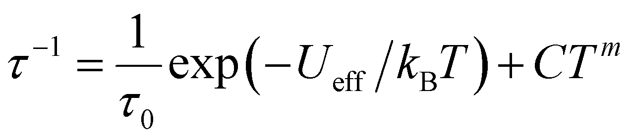
Fig. 4a and S13† show the temperature dependence of σ at various pressures based on six single-crystals. At ambient pressure, σ (=50–110 S cm−1 at 295 K) increased with a decrease in temperature, behaving as a metal above 62 K. Then σ decreased down to 32 K, then increased again up to σ = 400–650 S cm−1 at 6.5 K, and finally drastically decreased to σ = 560 S cm−1 at 2 K. The change ratio σ(2 K)/σ(300 K) was 5–10. The decrease in σ at ∼62 K was completely suppressed by coating the crystal with Apiezon N grease, which is known to induce a weak pressure effect of ∼0.03 GPa on the crystal. However, the decrease in σ at low temperature could not be suppressed even when pressures up to 2.0 GPa were applied. To investigate the origin of the anomaly at low temperature under σ, the magnetic field was swept between −9 T and 9 T. The magnetic field B was oriented perpendicular to the current direction with an angle θ between the magnetic field and conducting plane (ab plane) adjusted by the rotator probe (Fig. S14a and S14b†). MR is defined by the equation: MR (%) = [ρ(B,T) − ρ(0,T)]/ρ(0,T) × 100%, where ρ is the resistivity. Fig. 4b shows the MR effect under θ = 0° in the range of 2–100 K with symmetrical evolutions with respect to the field direction. The linear positive MR with 24% resistance increases at 2 K, and that with 2% resistance increases at 100 K in the field of 9 T. A negative MR was observed below 7.5 K in the low magnetic field region (Fig. 4c). In order to clarify whether the negative MR (θ = 0°) was caused by weak 2D localization or the interactions with the magnetic layer, the angle dependence of MR was examined. Fig. 4d shows the MR effect at θ = 90° in the range of 2–100 K. The linear positive MR with 11% resistance increases at 2 K and that with 0.7% resistance increased at 100 K under a 9 T field. Furthermore, a negative MR was observed below 5 K in the low magnetic field region (Fig. 4e). The negative MR was observed both perpendicular and parallel to the current at 2 K (Fig. 4f). A parallel magnetic field (θ = 90°) should have no effect on 2D localized electrons,23 however, a negative MR was also observed at 90° in contrast to the 2D localization model. This fact indicates that the decrease in σ observed below 6.5 K cannot be attributed to 2D weak localization. There must be interactions between the conducting and SMM layers in this temperature range.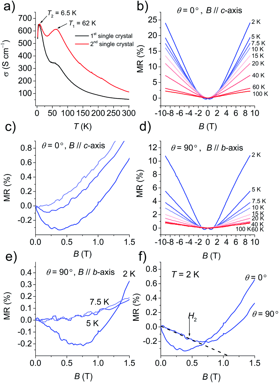 | ||
| Fig. 4 Electrical conductivity and magnetoresistance effects. (a) Temperature dependence of σ of two single-crystals using a standard four-probe technique. (b) Magnetic field dependence of MR at different temperatures with the magnetic field perpendicular to the 2D plane, θ = 0°, B‖c-axis. (c) MR–B plot in the range of 0–1.5 T at 2 K, 5 K and 7.5 K at θ = 0°. (d) Magnetic field dependence of MR at different temperatures with the magnetic field parallel to the 2D plane, θ = 90°, B‖b-axis. (e) MR–B plot in the range of 0–1.5 T at 2, 5 and 7.5 K with θ = 90°. (f) The MR–B plot in the range of 0–1.5 T at 2 K with θ = 0° and 90°. | ||
Electronic structure calculations
The electronic structure was calculated using DFT (Fig. 5) and extended Hückel tight-binding (EHTB) methods (Fig. S15†). The calculated results from the two methods agree with each other at least qualitatively. Fig. 5 shows the results from DFT-based density of state (DOS) and band structure calculations. The DOS has a small amount of BO electron density at the Fermi level, indicating that the BO layer has semimetallic characteristics. The total bandwidth is calculated to be 0.78 eV, which is close to that of the organic superconductor (BEDO-TTF)2ReO4·H2O.24 The bands of BO4 near the Fermi level mainly consist of eight HOMOs of the BO units, which are largely dispersed due to the effective HOMO overlap of the BO pairs in the “side” and “diagonal” directions (Fig. S16†). The undistinguished energy difference between the bands with up and down spin indicates the paramagnetic characteristic of the BO layer. The flat HOMO and HOMO-1 bands of the two Co units were mixed with the BO bands, causing hybridization between them. Thus, the angular momentum of the Co(3d) electrons could directly mix into that of the carrier (itinerant BO electrons) despite the small contribution of the Co(3d) orbitals to the HOMO. The Fermi level slightly cuts the conduction bands in ΓXY and ΓTU planes in the reciprocal lattice (high symmetry points are defined in Fig. S17†). There is almost no dispersion along the ΓZ direction, indicating that BO4 is a 2D conductor. In addition, near the symmetry points R and V, the valence and conduction bands take the shape of the upper and lower halves of a conical surface with tiny energy gaps, behaving as a semimetallic electronic structure (Fig. 5 and Fig. S18†). The Fermi surfaces, which are composed of two independent triangular-like hole tubes (Fig. S19†) and one unique quadrangular-like electron tube (Fig. S20†) and the symmetry-operation derived ones in the first Brillouin zone are shown in Fig. 6. This is because the intermolecular interaction is two-dimensional due to the I3-type BO packing, and the Fermi surfaces are arranged to give the distorted quadrilateral-like and triangular-like islands along the a–b direction due to the shape and size of the Brillouin zone. All electron and hole tubes are at the edge of the first Brillouin zone with one dependent hole tube along the ΓY direction, and the other hole tubes are aligned in the ΓV direction close to the electron tube without crossing. Thus, the results of the calculations indicate that BO4 is a 2D semimetal.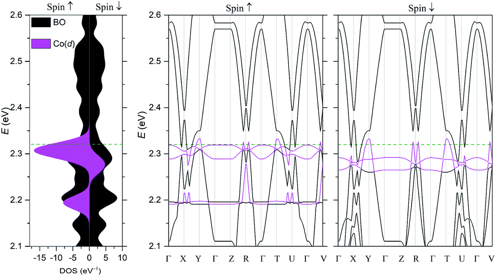 | ||
| Fig. 5 DFT calculations. Electronic band structure based on the crystal structure determined by using DFT calculations. High symmetry points in the crystal reciprocal lattice: Γ = (0, 0, 0), X = (0.5, 0, 0), Y = (0, 0.5, 0), Z = (0, 0, 0.5), R = (0.5, −0.5, 0.5), T = (0, 0.5, −0.5), U = (0.5, 0, −0.5), and V = (0.5, −0.5, 0). The Fermi energy level (green dashed line) is set at 2.32 eV. The magenta and black areas and curves indicate Co and BO electrons, respectively. | ||
 | ||
| Fig. 6 DFT calculations. Fermi surface of BO4 in an extended Brillouin zone, which is composed of electron (blue) and hole (red) pockets associated with the (Γ, X and Y) symmetry points in the bands. Black lines represent the first Brillouin zone, and green dotted lines represent the hidden 1D Fermi surface. | ||
Discussion
The most striking physical property of BO4 is the simultaneous manifestation of SMM nature and metallic σ. While σ shows semiconducting behaviour from 62 to 32 K and below 6.5 K, the temperature region for the metallic conduction includes the one for SMM behaviour (TB = 11 K). The Co(pdms)2 molecules are arranged in an ordered 2D narrow sheet (d = 7.2 Å), which causes the magnetic anisotropy of each Co(pdms)2 unit to be nearly aligned with the b-axis, affording a strong magnetic anisotropy. The ferromagnetic ordering observed between 10.2 K and 6.5 K is caused by weak intermolecular interactions between the Co(pdms)2 molecules due to the small rhombic angle in the magnetic layer. Subsequently, antiferromagnetic ordering was observed below 6.5 K assigned to the weak interactions between the SMM and conducting layers (d–π interactions). Thus, the weak inter- and intralayer interactions and the strong magnetic anisotropy maintain the SMM behaviour in a region of antiferromagnetic ordering. In other words, the Co(pdms)2 molecules are not significantly influenced by the surrounding Co ions, which essentially protects the SMM behaviour. On the other hand, we found that the TB of the Co(pdms)2 units significantly increased and the magnetic relaxation times increased below TN, which are caused by the interactions between conducting electrons and the SMM.For electron transport, the first decrease in σ at 62 K was suppressed by applying very low pressure (P = 0.03 GPa), which has been reported for several low dimensional organic metals,25 such as (BEDO-TTF)2ReO4·H2O and (TMTSF)2NO3, with a metal–insulator transition into a charge density wave (CDW) or spin density wave (SDW) state at low temperature.26 The σ value of (BEDO-TTF)2ReO4·H2O decreases several times due to the electronic instability involving the nesting of the hidden 1D Fermi surfaces (formed by the 2D hole and electron pockets).27BO4 has a similar arrangement of 2D Fermi surfaces of hole and electrons, and the decrease in σ at 62 K is ascribed to the formation of a CDW state due to the hidden 1D Fermi surface. The nesting of the 1D hidden Fermi surface along the ΓY direction (green dotted lines in Fig. 6) can effectively shrink a part of the Fermi surface in β′′-type 2D organic semimetals.28 However, some of the remaining Fermi surfaces continue to exhibit metallic behaviour at low temperature, as is the case for BO4 below 32 K. The conductivity in a 2D semimetal with 1D hidden nesting is very sensitive to the pressure, and even very weak pressure (∼0.03 GPa) is enough to induce a change in σ.29
The second decrease in σ below 6.5 K is insensitive to pressure. In this temperature range, a negative MR was observed for both perpendicular and parallel fields with respect to the conducting layer. Thus, the d–π interactions between the SMM and BO layers are important. Negative MRs were observed in fields perpendicular and parallel to the conducting layer up to ∼0.5 T, which is consistent with the characteristic spin–flop field (H2) in the MH curve. However, we should observe the corresponding distinct anomaly in the negative MR at the spin–flop transition (H2),30 and the absence of H2 in the MR measurement could be explained by the superposition of the largely positive MR enhanced by the peculiar semimetal-like electronic structure.
It is well known that a highly correlated electron system tends to adopt an antiferromagnetic insulating state.31 For the SMM layers, the TB of Co(pdms)2 was observed up to 11 K because of ferromagnetic coupling below 10.2 K. The increase in TB originates from the intrinsic ferromagnetic interactions. On the other hand, for the BO layers, the ab plane is metallic, and some electron density remains, although the partial nesting of the Fermi surface could occur. Thus, there is a possibility that the BO electrons are antiferromagnetically coupled with the SMM electrons along the b-axis below 6.5 K. Due to the two-dimensional conducting nature and strong magnetic anisotropy of the Co(d) electrons near the Fermi surfaces, synergetic effects could be observed. Furthermore, the presence of synergetic effects was supported by the low-temperature MR measurements where significant negative MR effects were observed in perpendicular and parallel directions.
Conclusions
Slow electrocrystallization of [Co(pdms)2]2− and neutral BEDO-TTF afforded β′-(BEDO-TTF)4 [Co(pdms)2]·3H2O (BO4), which showed the simultaneous manifestation of metallic conduction and SMM behaviours for the first time. Antiferromagnetic ordering mediated by π-electrons with SMMs was observed for the first time. By analysing the low-temperature magnetic phase transition and angle-dependence of magnetotransport, we found that the 2D conducting plane and strongly magnetic anisotropy played key roles in the synergetic effects in this layered material. From this aspect, SMMs have big advantages in molecule-based quantum spintronics compared to bulk magnets due to not only their high magnetic densities but also their strong magnetic anisotropies in SMMs. By combining them with high dimensional molecular conductors, such as two-dimensional BO and ET packing motifs, it is possible to observe such synergetic effects. Thus, from our studies on BO4, more stable metallic SMMs can be designed with the hope of producing superconducting SMM materials in the near future.Conflicts of interest
There are no conflicts to declare.Acknowledgements
This work was partially supported by CREST, JST grant number JPMJCR12L3. M. Y. acknowledges the support from the 111 Project (B18030) from China. H. Z. and C. H. thank Deutsche Forschungsgemeinschaft (DFG) for support via project 5675/6-1. H. Y. acknowledges the support by The Kyoto University Foundation.Notes and references
- S. M. Mukhopadhyay. Nanoscale multifunctional materials science and applications. John Wiley & Sons, Inc. 2012 Search PubMed.
- (a) E. Coronado, J. R. Galan-Mascaros, C. J. Gomez-Garcia and V. Laukhin, Nature, 2000, 408, 447–449 CrossRef CAS; (b) N. D. Kushch, E. B. Yagubskii, M. V. Kartsovnik, L. I. Buravov, A. D. Dubrovskii, A. N. Chekhlov and W. Biberacher, J. Am. Chem. Soc., 2008, 130, 7238 CrossRef CAS; (c) H. Fujiwara, E. Fujiwara, Y. Nakazawa, B. Z. Narymbetov, K. Kato, H. Kobayashi, A. Kobayashi, M. Tokumoto and P. Cassoux, J. Am. Chem. Soc., 2001, 123, 306–314 CrossRef CAS; (d) M. Kurmoo, A. W. Graham, P. Day, S. J. Coles, M. B. Hursthouse, J. L. Caulfield, J. Singleton, F. L. Pratt, W. Hayes, L. Ducasse and P. Guionneau, J. Am. Chem. Soc., 1995, 117, 12209–12217 CrossRef CAS; (e) H. Kobayashi, H. B. Cui and A. Kobayashi, Chem. Rev., 2004, 104, 5265–5288 CrossRef CAS; (f) S. Uji, H. Shinagawa, T. Terashima, T. Yakabe, Y. Terai, M. Tokumoto, A. Kobayashi, H. Tanaka and H. Kobayashi, Nature, 2001, 410, 908–910 CrossRef CAS.
- M. N. Baibich, J. M. Broto, A. Fert, F. N. Vandau, F. Petroff, P. Eitenne, G. Creuzet, A. Friederich and J. Chazelas, Phys. Rev. Lett., 1988, 61, 2472–2475 CrossRef CAS.
- G. Binasch, P. Grünberg, F. Saurenbach and W. Zinn, Phys. Rev. B: Condens. Matter Mater. Phys., 1989, 39, 4828–4830 CrossRef CAS.
- Y. B. Shen, G. Cosquer, B. K. Breedlove and M. Yamashita, Magnetochemistry, 2016, 2, 44 CrossRef.
- X. Zhang, H. M. Xie, M. Ballesteros-Rivas, T. J. Woods and K. R. Dunbar, Chem.–Eur. J., 2017, 23, 7448–7452 CrossRef CAS.
- (a) H. Hiraga, H. Miyasaka, K. Nakata, T. Kajiwara, S. Takaishi, Y. Oshima, H. Nojiri and M. Yamashita, Inorg. Chem., 2007, 46, 9661–9671 CrossRef CAS; (b) H. Hiraga, H. Miyasaka, S. Takaishi, T. Kajiwara and M. Yamashita, Inorg. Chim. Acta, 2008, 361, 3863–3872 CrossRef CAS; (c) H. Hiraga, H. Miyasaka, R. Clerac, M. Fourmique and M. Yamashita, Inorg. Chem., 2009, 48, 2887–2898 CrossRef CAS; (d) K. Kubo, H. Miyasaka and M. Yamashita, Physics B, 2010, 405, 313–316 CrossRef; (e) K. Kubo, T. Shiga, T. Yamamoto, A. Tajima, T. Morikawa, Y. Ikemoto, H. Miyasaka, M. Yamashita, E. Sessine, M. L. Mercuri, P. Deplano, Y. Nakazawa and R. Kato, Inorg. Chem., 2011, 50, 9337–9344 CrossRef CAS.
- (a) R. Sessoli, D. Gatteschi, A. Caneschi and M. A. Novak, Nature, 1993, 365, 141–143 CrossRef CAS; (b) N. Ishikawa, M. Sugita, T. Ishikawa, S. Koshihara and Y. Kaizu, J. Am. Chem. Soc., 2003, 125, 8694–8695 CrossRef CAS.
- D. N. Woodruff, R. E. P. Winpenny and R. A. Layfield, Chem. Rev., 2013, 113, 5110–5148 CrossRef CAS.
- L. Bogani and W. Wernsdorfer, Nat. Mater., 2008, 7, 179–186 CrossRef CAS.
- K. Sato, E. Saitoh, A. Willoughby, P. Capper and S. Kasap. Spintronics for next generation innovative devices. John Wiley & Sons, lnc. 2015 Search PubMed.
- G. Cosquer, Y. B. Shen, M. Almeida and M. Yamashita, Dalton Trans., 2018, 47, 7616–7627 RSC.
- Y. B. Shen, G. Cosquer, H. Ito, D. C. Izuogu, A. J. W. Thom, T. Ina, T. Uruga, T. Yoshida, S. Takaishi, B. K. Breedlove, Z. Y. Li and M. Yamashita, Angew. Chem., Int. Ed., 2020, 59, 2399–2406 CrossRef CAS.
- (a) S. Kahlich, D. Schweitzer, I. Heinen, S. E. Lan, B. Nuber, H. J. Keller, K. Winzer and H. W. Helberg, Solid State Commun., 1991, 80, 191–195 CrossRef CAS; (b) E. Coronado, C. Gimenez-Saiz, C. J. Gomez-Garcia and S. C. Capelli, Angew. Chem., Int. Ed., 2004, 43, 3022–3025 CrossRef CAS.
- (a) F. Wudl, H. Yamochi, T. Suzuki, H. Isotalo, C. Fite, H. Kasmai, K. Liou, G. Srdanov, P. Coppens, K. Maly and A. Frostjensen, J. Am. Chem. Soc., 1990, 112, 2461–2462 CrossRef CAS; (b) S. Horiuchi, H. Yamochi, G. Saito, K. Sakaguchi and M. Kusunoki, J. Am. Chem. Soc., 1996, 118, 8604–8622 CrossRef CAS.
- (a) N. D. Kushch, L. I. Buravov, P. P. Kushch, G. V. Shilov, H. Yamochi, M. Ishikawa, A. Otsuka, A. A. Shakin, O. V. Maximova, O. S. Volkova, A. N. Vasiliev and E. B. Yagubskii, Inorg. Chem., 2018, 57, 2386–2389 CrossRef CAS; (b) O. M. Vyaselev, N. D. Kushch, E. B. Yagubskii, O. V. Maximova and A. N. Vasiliev, Phys. Rev. B, 2020, 101 Search PubMed.
- T. Mori, Bull. Chem. Soc. Jpn., 1998, 71, 2509–2526 CrossRef CAS.
- N. Drichko, R. Vlasova, V. Semkin, A. Graja, O. A. Bogdanova, E. Zhilyaeva and R. N. Lyubovskaya, Synth. Met., 2000, 109, 123–127 CrossRef CAS.
- O. Drozdova, H. Yamochi, K. Yakushi, M. Uruichi, S. Horiuchi and G. Saito, J. Am. Chem. Soc., 2000, 122, 4436–4442 CrossRef CAS.
- Y. Rechkemmer, F. D. Breitgoff, M. van der Meer, M. Atanasov, M. Hakl, M. Orlita, P. Neugebauer, F. Neese, B. Sarkar and J. van Slageren, Nat. Commun., 2016, 7, 10467 CrossRef CAS.
- G. Saito and Y. Yoshida, Bull. Chem. Soc. Jpn., 2007, 80, 1–137 CrossRef CAS.
- A. A. Fraerman and M. V. Sapozhnikov, J. Magn. Magn. Mater., 1999, 192, 191–200 CrossRef CAS.
- (a) Y. Ishizaki, M. Izumi, H. Ohnuki, K. Kalita-Lipinska, T. Imakubo and K. Kobayashi, Phys. Rev. B: Condens. Matter Mater. Phys., 2001, 63, 134201 CrossRef; (b) Y. Ishizaki, M. Izumi, H. Ohnuki, T. Imakubo and K. Kalita-Lipinska, Colloids Surf., A, 2002, 198, 723–728 CrossRef.
- W. Sommer, J. Moldenhauer, D. Schweitzer, I. Heinen and H. J. Keller, Synth. Met., 1995, 68, 133–139 CrossRef CAS.
- (a) M. H. Whangbo and E. Canadell, J. Am. Chem. Soc., 1992, 114, 9587–9600 CrossRef CAS; (b) D. Jerome, Chem. Rev., 2004, 104, 5565–5591 CrossRef CAS.
- (a) S. Kahlich, D. Schweitzer, C. Rovira, J. A. Paradis, M. H. Whangbo, I. Heinen, H. J. Keller, B. Nuber, P. Bele, H. Brunner and R. P. Shibaeva, Z. Phys. B: Condens. Matter, 1994, 94, 39–47 CrossRef CAS; (b) S. Tomic, J. R. Cooper, D. Jerome and K. Bechgaard, Phys. Rev. Lett., 1989, 62, 462–465 CrossRef CAS.
- M. H. Whangbo, E. Canadell, P. Foury and J. P. Pouget, Science, 1991, 252, 96–98 CrossRef CAS.
- M. H. Whangbo, J. Ren, W. Liang, E. Canadell, J. P. Pouget, S. Ravy, J. M. Williams and M. A. Beno, Inorg. Chem., 1992, 31, 4169–4173 CrossRef CAS.
- (a) S. Kahlich, D. Schweitzer, P. Aubansenzier, D. Jerome and H. J. Keller, Solid State Commun., 1992, 83, 77–79 CrossRef CAS; (b) S. Kahlich, D. Schweitzer, P. Aubansenzier, D. Jerome and H. J. Keller, Synth. Met., 1993, 56, 2483–2488 CrossRef CAS.
- T. Hayashi, X. Xiao, H. Fujiwara, T. Sugimoto, H. Nakazumi, S. Noguchi, T. Fujimoto, S. Yasuzuka, H. Yoshino, K. Murata, T. Mori and H. Aruga-Katori, J. Am. Chem. Soc., 2006, 128, 11746–11747 CrossRef CAS.
- D. Jerome, Science, 1991, 252, 1509–1514 CrossRef CAS.
Footnote |
| † Electronic supplementary information (ESI) available. CCDC 1970380. For ESI and crystallographic data in CIF or other electronic format see DOI: 10.1039/d0sc04040a |
| This journal is © The Royal Society of Chemistry 2020 |