
 Open Access Article
 This Open Access Article is licensed under a
 Creative Commons Attribution 3.0 Unported Licence
Revealing the relationship between photoelectrochemical performance and interface hole trapping in CuBi2O4 heterojunction photoelectrodes†
Angang
Song
 ab,
Igal
Levine
c,
Roel
van de Krol
ab,
Thomas
Dittrich
*c and
Sean P.
Berglund
*a
ab,
Igal
Levine
c,
Roel
van de Krol
ab,
Thomas
Dittrich
*c and
Sean P.
Berglund
*a
aInstitute for Solar Fuels, Helmholtz-Zentrum Berlin für Materialien und Energie GmbH, Hahn-Meitner-Platz 1, 14109 Berlin, Germany. E-mail: sean.berglund@gmail.com
bInstitut für Chemie, Technische Universität Berlin, Straße des 17. Juni 124, 10623 Berlin, Germany
cInstitute for Silicon Photovoltaics, Helmholtz-Zentrum Berlin für Materialien und Energie GmbH, Kekuléstr. 5, 12489 Berlin, Germany. E-mail: dittrich@helmholtz-berlin.de
First published on 14th September 2020
Abstract
p-Type CuBi2O4 is considered a promising metal oxide semiconductor for large-scale, economic solar water splitting due to the optimal band structure and low-cost fabrication. The main challenge in utilizing CuBi2O4 as a photoelectrode for water splitting, is that it must be protected from photo-corrosion in aqueous solutions, an inherent problem for Cu-based metal oxide photoelectrodes. In this work, several buffer layers (CdS, BiVO4, and Ga2O3) were tested between CuBi2O4 and conformal TiO2 as the protection layer. RuOx was used as the co-catalyst for hydrogen evolution. Factors that limit the photoelectrochemical performance of the CuBi2O4/TiO2/RuOx, CuBi2O4/CdS/TiO2/RuOx, CuBi2O4/BiVO4/TiO2/RuOx and CuBi2O4/Ga2O3/TiO2/RuOx heterojunction photoelectrodes were revealed by comparing photocurrents, band offsets, and directed charge transfer measured by modulated surface photovoltage spectroscopy. For CuBi2O4/Ga2O3/TiO2/RuOx photoelectrodes, barriers for charge transfer strongly limited the performance. In CuBi2O4/CdS/TiO2/RuOx, the absence of hole traps resulted in a relatively high photocurrent density and faradaic efficiency for hydrogen evolution despite the presence of pronounced deep defect states at the CuBi2O4/CdS interface. Hole trapping limited the performance moderately in CuBi2O4/BiVO4/TiO2/RuOx and strongly in CuBi2O4/TiO2/RuOx photoelectrodes. For the first time, our results show that hole trapping is a key factor that must be addressed to optimize the performance of CuBi2O4-based heterojunction photoelectrodes.
Introduction
Copper bismuth oxide (CuBi2O4) is a promising photoabsorber for photoelectrochemical (PEC) water splitting due to its optimal optical bandgap (1.5–1.8 eV), positive photocurrent onset potential (more positive than 1 V vs. RHE), and Earth-abundant chemical composition.1–4 However, several limitations in CuBi2O4 must be overcome to improve its performance as a photocathode for the hydrogen evolution reaction. Perhaps the greatest limitation of CuBi2O4 is its susceptibility to photo-corrode under illumination in aqueous solutions, which is a common problem for Cu-based metal oxide photoelectrodes.5–8 Surface modification via the formation of a heterojunction with a suitable buffer layer and/or an n-type protection layer could be highly effective at overcoming this limitation of CuBi2O4 based on previous reports on other Cu-based metal oxide photocathodes such as Cu2O, CuO and CuFeO4 as well as Si-based photoelectrodes.9–13To be effective, a suitable buffer layer and/or protective layer must cover CuBi2O4 conformally without any pinholes and have energy band positions that match favorably to allow for efficient transport of charge carriers across the solid-state and semiconductor–electrolyte interfaces. TiO2 deposited by atomic layer deposition (ALD) has been reported as an excellent protective layer for unstable photoelectrodes while simultaneously allowing for efficient electron transfer to the electrolyte under the PEC conditions for hydrogen evolution.11,14–16 Studies have shown that TiO2-protected Cu2O-based photocathodes exhibit a relatively high photocurrent density and significantly enhanced stability when using various buffer layers between Cu2O and TiO2 such as ZnO and Al doped ZnO (AZO).15,17,18 However, relatively poor photocurrent onset potentials (0.45–0.55 V vs. RHE) were obtained in this structure due to the small photovoltage produced by the heterojunctions. It has been shown that the use of ZnS as a buffer layer between Cu2O and TiO2 can increase the photovoltage at the multilayer/electrolyte junction thereby shifting the onset potential cathodically to 0.7 V vs. RHE.19 The introduction of Ga2O3 as a buffer layer between Cu2O and TiO2 can improve the photovoltage even further (open-circuit voltage up to 1.2 V for Cu2O solar cells20 and photocurrent onset above 1.0 V vs. RHE for photocathodes).21–23 In another work for CuO-based heterojunction photocathodes, ZnO showed rather poor performance as a buffer layer, in contrast to CdS.24
The band positions of the various layers within TiO2-protected heterojunction photocathodes are crucial in determining the overall performance. The photovoltage of the device is ultimately limited by the difference in the Fermi level of the photoabsorber and the conduction band of either the buffer layer or the TiO2 protective layer, depending on which has a lower conduction band.5 Furthermore, numerous studies have emphasized the importance of band alignment between the photoabsorber and the buffer layer. In addition to band alignment, other key factors related to recombination and/or trapping at the layer interfaces can contribute to the overall performance. For example, it was recently shown by model calculations that Al-doped ZnO (AZO) buffer layers between Cu2O and TiO2 should enable a higher photovoltage than Ga2O3 buffer layers, but AZO may induce an interface recombination layer that hinders charge transfer and thus decreases the photovoltage.9 Therefore, in addition to optimal band energy alignment, heterojunction interface layers must be high-quality and possess low interfacial trap densities to maximize device performance. Incidentally, compared to band positions, defect states and recombination sites at interfaces are often more difficult to characterize. Modulated surface photovoltage (SPV) spectroscopy can be used to provide information about electronic transitions from which photogeneration can take place and about the direction of charge separation even over very short distances and with very high sensitivity.25,26
In order to obtain information about dominant limiting factors in heterojunction photoelectrodes with CuBi2O4 as the absorber layer and ALD-deposited TiO2 as the protective layer, we compared how different buffer layers (CdS, BiVO4, and Ga2O3) affected the photocurrent density (with RuOx as a co-catalyst layer for H+ reduction reaction) as well as the behavior of modulated SPV spectra. Fig. 1 shows the layer stacking of the various heterojunction photoelectrodes that were tested in this work. The energy positions of the valence band edges in the separate layers were measured by photoelectron spectroscopy. Our results show that, in addition to suitable band alignment for charge transfer, preferential trapping of holes at CuBi2O4/TiO2, CuBi2O4/BiVO4 and CuBi2O4/Ga2O3 interfaces drastically limits the photocurrent of the corresponding PEC systems. In contrast, preferential trapping of electrons at the CuBi2O4/CdS interface limits the photocurrent to a much lesser extent despite the appearance of pronounced deep defect states.
 | ||
Fig. 1 Schematic of the layer stacking for the heterojunction photoelectrodes analyzed in this work. A TiO2 protection layer was used in all cases, which was deposited either directly on the CuBi2O4 absorber, or on the Ga2O3, BiVO4, or CdS buffer layer. RuOx was used as a co-catalyst for the hydrogen evolution reaction. The substrate was SnO2![[thin space (1/6-em)]](https://www.rsc.org/images/entities/char_2009.gif) :F, fluorine-doped tin oxide (FTO). :F, fluorine-doped tin oxide (FTO). | ||
Results and discussion
Photoelectrochemical analysis
In this work we performed PEC measurements on bare CuBi2O4 photocathodes in addition to the CuBi2O4/CdS/TiO2/RuOx, CuBi2O4/Ga2O3/TiO2/RuOx, CuBi2O4/BiVO4/TiO2/RuOx and CuBi2O4/TiO2/RuOx heterojunction photoelectrodes. They were measured under chopped AM 1.5 illumination in 0.3 M K2SO4 and 0.2 M phosphate buffer (pH 6.8) with Ar bubbling to purge dissolved oxygen from the electrolyte. As shown in Fig. S1a in the ESI,† the bare CuBi2O4 electrode exhibited a relatively large cathodic photocurrent density of −1 mA cm−2 at 0.4 V vs. RHE under visible light illumination for the chopped linear sweep voltammetry (LSV) measurement. However, the photocurrent density decayed rapidly, as shown in the constant potential measurement under illumination at 0.6 V vs. RHE (see Fig. S1b†). Based on previous reports this is attributed to the reduction of Cu2+ to Cu1+ and/or Cu in aqueous solution.1,27–29 After 30 minutes the photocurrent density was only 6.4% of the initial value and by the end of the 5 hour measurement the illuminated area of the photoelectrode was transparent (see the inset of Fig. S1b†) presumably because the reduced copper dissolved into the electrolyte. Differential mass spectrometry (DEMS) measurements confirmed that the bare CuBi2O4 photocathodes did not produce a detectable amount of hydrogen (see Fig. S1c†).The chopped LSV curves for the CuBi2O4/CdS/TiO2/RuOx, CuBi2O4/Ga2O3/TiO2/RuOx, CuBi2O4/BiVO4/TiO2/RuOx and CuBi2O4/TiO2/RuOx heterojunction photoelectrodes are shown in Fig. 2a. Unlike the bare CuBi2O4 photocathode, the heterojunction photoelectrodes showed minimal dark currents at potentials more negative than 0.35 V vs. RHE, indicating that the ALD-deposited TiO2 layer effectively inhibits the electrochemical corrosion of the underlying CuBi2O4. However, the photocurrent generated from the CuBi2O4/TiO2/RuOx and CuBi2O4/Ga2O3/TiO2/RuOx photocathodes (blue and black lines) were very small (ca. −0.04 mA cm−2 and −0.01 mA cm−2 at 0 V vs. RHE, respectively). This indicates that the CuBi2O4/TiO2 and the CuBi2O4/Ga2O3 or Ga2O3/TiO2 interfaces in these samples do not effectively charge transport to the RuOx co-catalyst layer and into the electrolyte. The CuBi2O4/BiVO4/TiO2/RuOx photoelectrode (green line) shows significantly higher photocurrent density (ca. −0.5 mA cm−2 at 0 V vs. RHE) while the CuBi2O4/CdS/TiO2/RuOx photoelectrode (red line) shows by far the highest photoactivity with a plateau in photocurrent density at ca. −1 mA cm2 at 0 V vs. RHE. It also has the most positive photocurrent onset at 0.8 V vs. RHE. For the CuBi2O4/CdS/TiO2/RuOx photoelectrode the bump in the dark current around 0.5–0.6 V vs. RHE is likely due to the reduction of dissolved oxygen that could not be completely purged from the PEC cell by Ar bubbling,5 or another reduction process on the electrode surface such as the pre-reduction of the RuOx catalyst.16 The DEMS measurement (Fig. 2b) shows that when the photocurrent increases cathodically at potentials negative of 0.3 V vs. RHE (red line) there is a simultaneous increase in H2 signal (black line) confirming that the CuBi2O4/CdS/TiO2/RuOx heterojunction photoelectrode can evolve hydrogen photoelectrochemically. The faradaic efficiency was estimated to be 92% based on calibration of the DEMS using a Pt metal electrode.
 | ||
| Fig. 2 (a) Chopped LSV scans for a CuBi2O4/CdS/TiO2/RuOx (red), CuBi2O4/BiVO4/TiO2/RuOx (green), CuBi2O4/Ga2O3/TiO2/RuOx (black) and CuBi2O4/TiO2/RuOx photocathode (blue) under simulated AM1.5 illumination (these are representative measurements of at least 4 samples for each condition). (b) Differential electrochemical mass spectrometry (DEMS) LSV scans for a CuBi2O4/CdS/TiO2/RuOx photocathode with illumination by a xenon lamp, showing current (red) and H2 signal (black). Measurements were performed in three-electrode configuration in 0.3 M K2SO4 and 0.2 M phosphate buffer electrolyte (pH 6.8) with Ar bubbling. | ||
Note that the photocurrent density directly before the onset of dark current from electrochemical proton reduction (ca. −1 mA cm2 at 0 V vs. RHE in Fig. 2a) is close to the maximum photocurrent density for bare CuBi2O4 before the onset of dark current from electrochemical corrosion (ca. −1 mA cm−2 at 0.4 V vs. RHE in Fig. S1a†). This implies that most of the electrons that are photogenerated in CuBi2O4, which previously participated in the corrosion reaction (Cu2+ → Cu1+ and/or Cu), are successfully injected into the CdS buffer and TiO2 protection layers, and eventually into the electrolyte to drive the hydrogen evolution reaction.
In order to investigate the long-term stability of the CuBi2O4/CdS/TiO2/RuOx photocathodes, the photocurrent density was measured at a constant potential of 0.0 V vs. RHE for 5 hours with intermittent chopping of the front illumination (see Fig. S2 in the ESI†). The measurement shows a decay in photocurrent which was more than 100 times slower than for the bare CuBi2O4 photocathode (Fig. S1b†). A significant part of the decay was attributed to deterioration of the RuOx co-catalyst as demonstrated by partial restoration of the photocurrent after re-deposition of RuOx after 3 hours. At the end of the 5 hour measurement, and after the single re-deposition of the RuOx co-catalyst, 30% of the initial photocurrent density was preserved. Visually the illuminated area of the CuBi2O4/CdS/TiO2/RuOx photoelectrode was almost indistinguishable from the non-illuminated area (see the inset of Fig. S2†). Under scanning electron microscope (SEM) there were no significant morphological differences between areas of the sample that were and were not PEC tested other than a slight smoothing of the electrode surface after PEC testing (see Fig. S3†). Therefore, the ALD-deposited TiO2 layer effectively blocked the contact between CuBi2O4 and the aqueous electrolyte and hindered photo-corrosion. This was also the case for the other layer systems. For comparison, photos and SEM images of the CuBi2O4/CdS/TiO2, CuBi2O4/Ga2O3/TiO2 and CuBi2O4/BiVO4/TiO2 photoelectrodes are shown in Fig. S4–S6,† respectively.
Band alignment
In order to estimate the band positions of the different materials in the heterojunction photoelectrodes, the energy band offsets were measured through a combination of X-ray photoelectron spectroscopy (XPS), ultraviolet photoelectron spectroscopy (UPS), UV-visible spectrophotometry, and Mott–Schottky analysis (including work from previous studies). Fig. S7a† shows the XPS spectrum for Cu at the surface of bare CuBi2O4. There are two main peaks at 933.8 and 953.6 eV corresponding to the Cu 2p3/2 and 2p1/2 levels, both of which were attributed to the presence of the Cu2+ state on the surface.30 The binding energies of Cd 3d, Ga 3d, V 2p and Ti 2p core levels of CdS, Ga2O3, BiVO4 and TiO2 are measured to be 406.3, 21.2, 516.7 and 459.3 eV, respectively (see Fig. S7b–e†). Fig. S8† shows the XPS survey results for the stack samples of the CuBi2O4/CdS/TiO2, CuBi2O4/Ga2O3/TiO2, CuBi2O4/BiVO4/TiO2 and CuBi2O4/TiO2. The presence of strong Ti peaks and the absence of Cu, Cd, Ga and V peaks in the survey spectra indicates that the ALD-deposited TiO2 layer fully covers the buffer layers.For the band positions of bare CuBi2O4, we used our previously reported values from Mott–Schottky analysis and UPS measurements, to estimate a conduction band (EC) of −0.3 V vs. RHE and a valence band (EV) of 1.2 V vs. RHE.4,5,31 The flat-band potential (φfb) of our spray-deposited BiVO4 films is 0.37 V vs. RHE,5,32 which can then be used to estimate the Fermi level (EF) while taking into account the potential drop across the Helmholtz layer.5,33 Fig. S9a–c† show the UPS spectra of CdS, Ga2O3 and TiO2 thin films on FTO substrate measured with a 2 V bias. The work function (Φ), defined as the difference between the vacuum energy level and Fermi level (EF), can be derived from the low kinetic energy cut-off in the secondary emission feature. The photon energy of the UV source (He I discharge) was 21.21 eV. Given that the Fermi level at the surface of these overlayers is considered independently of the spectrometer, the work function is determined to be 21.21 – 2 – secondary emission cut-off (SEC). The work function of CdS, Ga2O3 and TiO2 thin films are calculated to be 4.12, 3.63 and 4.57 eV, respectively. Using 4.5 eV vs. vacuum as the reference value for the electrochemical proton reduction (0.0 V vs. RHE) we can estimate the Fermi energies of the CdS, Ga2O3 and TiO2 layers at approximately −0.38, −0.87 and 0.07 V vs. RHE, respectively. These values are in agreement with the literature.34–36
The valence band positions with respect to the position of the Fermi level, EF − EV, were determined by linear extrapolation of the UPS spectrum at the low binding energy side to the binding energy axis (see Fig. S10†). EF − EV for CdS, BiVO4, Ga2O3 and TiO2 thin films are calculated to be 2.5, 2.4, 4.6, and 3.3 eV, respectively, which is consistent with previously reported values.37,38 Since CdS has a bandgap of 2.4–2.5 eV this would place the conduction band very close to the Fermi level at −0.38 V vs. RHE, which is within the wide range of previously reported EC values for CdS.5,39,40 The experimentally determined band energy values for all samples are summarized in Table S1 in the ESI† along with values from the literature.
Using the values given in Table S1,† the energies of conduction and valence bands were obtained and illustrated in Fig. 3 for the individual layers in the CuBi2O4/CdS/TiO2, CuBi2O4/Ga2O3/TiO2 and CuBi2O4/BiVO4/TiO2 heterojunction photoelectrodes in relation to the electrochemical redox potentials for proton reduction (H+/H2) and water oxidation (H+, O2/H2O) at 0.0 and 1.23 V vs. RHE, respectively. Since the conduction band of CuBi2O4 is at −0.3 V vs. RHE and the Fermi level of TiO2 is at approximately 0.0 V vs. RHE, all of the heterojunctions shown in Fig. 3 should be thermodynamically capable of reducing H+ as long as photogenerated electrons can be transported to the TiO2 surface. However, there are differences in the conduction band offsets between CuBi2O4 and each buffer layer (ΔEC,1) and between TiO2 and each buffer layer (ΔEC,2). For a wide range of heterojunctions, including CuO/TiO2 junctions, it has been shown that a high conduction band offset can promote high interface recombination and therefore inhibit charge transport.41 Better band alignment of the CuBi2O4/buffer layer provides a larger driving force for charge transport in CuBi2O4, results in a smaller concentration of holes near the interface and reduces the interfacial recombination. For all of the systems shown in Fig. 3, ΔEC,1 is by far the smallest between CuBi2O4 and CdS (less than 0.2 eV) while it is approximately 0.57 eV between CuBi2O4 and BiVO4 and –0.67 eV between CuBi2O4 and Ga2O3 assuming that EC is approximately 0.1 eV above EF in the buffer layers. The significantly higher conduction band of Ga2O3 compared to CuBi2O4 creates an energy barrier, thus significantly limiting the charge separation efficiency and the injection of the photogenerated electrons to the TiO2, which increases the recombination rate of photogenerated electrons and holes at the CuBi2O4/Ga2O3/TiO2 interfaces, especially if they contain defect states. This alone is enough to explain the poor performance of the CuBi2O4/Ga2O3/TiO2/RuOx photoelectrode compared to the others. For all of the heterojunctions shown in Fig. 3, ΔEC,2 is also smallest with CdS as the buffer layer. For the CuBi2O4/BiVO4/TiO2 system, transport of photogenerated electrons from CuBi2O4 to BiVO4 is thermodynamically favorable, but the ΔEC,2 value of −0.27 eV may hinder transport of these electrons into TiO2. Overall, the relatively small conduction band offsets between CuBi2O4, CdS, and TiO2 makes the CuBi2O4/CdS/TiO2 heterojunction photoelectrode more favorable for obtaining a high photovoltage and transporting charges compared to the CuBi2O4/Ga2O3/TiO2/RuOx and CuBi2O4/BiVO4/TiO2/RuOx photoelectrodes.
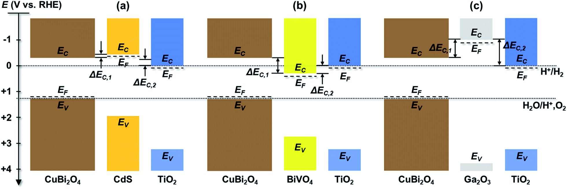 | ||
| Fig. 3 Estimated band diagrams for systems containing (a) CuBi2O4/CdS/TiO2, (b) CuBi2O4/BiVO4/TiO2 and (c) CuBi2O4/Ga2O3/TiO2 in relation to electrochemical redox potentials for proton reduction (H+/H2) and water oxidation (H+, O2/H2O). EF is the Fermi level, EC is the conduction band, EV is the valence band, and ΔEC,1 and ΔEC,2 are the conduction band offsets. | ||
Based on these energy band diagrams the CuBi2O4/TiO2/RuOx photoelectrode is also expected to contain a relatively small band offset of approximately 0.3 eV between CuBi2O4 and TiO2. Therefore, assuming negligible formation of interface dipoles, the performance of the CuBi2O4/TiO2/RuOx photoelectrode is expected to be comparable to CuBi2O4/CdS/TiO2/RuOx and higher than the CuBi2O4/BiVO4/TiO2/RuOx heterojunction system. As shown in Fig. 2a, this is clearly not the case, suggesting that additional factors aside the band offsets probably play an important role in the heterojunction systems. One of these factors, common in the case of heterojunctions, is the formation of intermixed interface layers, which may serve as hole or electron traps and hinder charge transfer.
Surface photovoltage analysis
To understand the relation between the charge transfer kinetics in the various heterojunctions and their PEC performance, modulated surface photovoltage (SPV) spectroscopy in the fixed capacitor arrangement was utilized.26 Aside from its very high sensitivity, modulated SPV spectroscopy can provide information about fast and slow (or retarded) processes in relation to the modulation period. Modulated SPV spectra are measured with double-phase lock-in amplifiers. The in-phase (x) and phase-shifted by 90° (y) signals are related to the fast and slow responses, respectively. In general, the response times of the SPV are much shorter (or longer) than the modulation period after switching on and off illumination if y (or x) are equal to 0. Furthermore, positive (or negative) x-signals are related to preferential separation of photogenerated electrons towards the bulk (or surface) of the absorber. The sign of the y-signal in relation to the sign of the x-signal gives information about the preferential direction of trapped charge carriers. If the x- and y-signals are of opposite sign, the direction of separated trapped charge carriers is similar to that of fast charge separation and relaxation. In contrast, if the x- and y-signals have the same sign, the directions of separated charge carriers are opposite for the dominating fast and slow processes (see Fig. S11† for a schematic illustration, and for more detailed explanations also paragraph 2.3.4. in ref. 26 or the ESI in ref. 42).To start, in order to compare between the different samples in terms of their general SPV response (not separated to slow and fast components), the x- and y-signals can be converted into amplitudes. The amplitude is defined as the square root of the sum of the squared x- and y-signals. The amplitude spectra of the CuBi2O4/CdS/TiO2, CuBi2O4/BiVO4/TiO2, CuBi2O4/TiO2 and CuBi2O4/Ga2O3/TiO2 systems are presented on a semi-log scale in Fig. 4. The extracted band gap of CuBi2O4, which is determined close to where the SPV deviates from exponential dependance, amounts to 1.55–1.6 eV, in agreement with our previous report.5 When comparing the maximum measured SPV amplitudes, we find that there is no direct correlation between the maximum SPV signal and the PEC performance, i.e. for the CuBi2O4/TiO2 sample, the maximum SPV amplitude is the highest, however for this sample very low photocurrent values were obtained compared to the samples containing CdS or BiVO4 buffer layers (see Fig. 2a). Analysis of the amplitude signals below the bandgap can yield valuable information regarding tail states and other defect states in the bulk of the absorber as well as in the interfaces with the different protection layers. If assuming that charge separation is caused only by directed transport of mobile charge carriers in delocalized states, and the SPV measurements are performed in the low-signal case and under homogeneous absorption within the charge separation and/or diffusion lengths, and the x- and y-signals do not change their signs within the corresponding spectral range, an exponential increase of the amplitude near the band gap or the first derivative of a logistic growth function are directly related to the exponential distribution of states near the valence (or conduction) band edge or to the distribution of deep defect states, respectively, from which photogeneration into delocalized states takes place.
 | ||
| Fig. 4 Amplitude spectra of CuBi2O4/CdS/TiO2, CuBi2O4/BiVO4/TiO2, CuBi2O4/TiO2 and CuBi2O4/Ga2O3/TiO2 (black squares, red circles, blue triangles and green stars, respectively). The solid green and red, blue, and black lines are fits below the band gap with one exponential term, the sum of two exponential terms, and the sum of a logarithmic growth and an exponential function for CuBi2O4/Ga2O3/TiO2 and CuBi2O4/BiVO4/TiO2, CuBi2O4/TiO2, and CuBi2O4/CdS/TiO2, respectively. The two vertical dashed lines mark the approximate band gap range of CuBi2O4. | ||
Thus, under the above assumptions, we find the following fitting functions were needed to obtain a good fit, depending on the sample:
 | (1) |
 | (2) |
 | (3) |
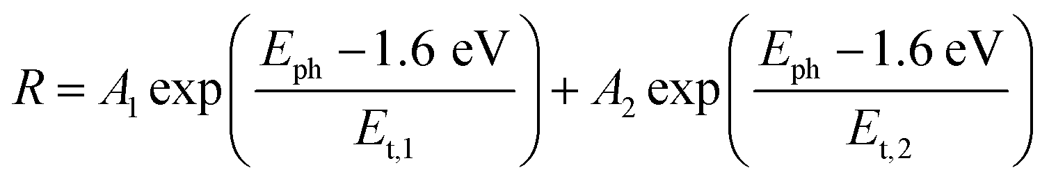
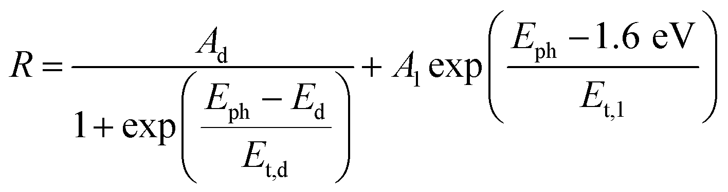
For the CuBi2O4/BiVO4/TiO2 and CuBi2O4/Ga2O3/TiO2 samples, a single exponential term (eqn (1)) was sufficient. For the CuBi2O4/TiO2, a sum of two exponential terms was required (eqn (2)), and for the CuBi2O4/CdS/TiO2 a sum of a logarithmic growth and an exponential function was required (eqn (3)). An identical band gap of 1.6 eV was used for all fits of the increasing part of the amplitude spectra. The main, common exponentials (eqn (1)) were characterized by the same tail energy (Et,1) equal to 83 meV in all equations (we note that Et is related, yet not equal to the so-called Urbach tail which is experimentally obtained from optical absorption). This gives evidence that Et,1 is related to disorder-induced defect states near the band gap of the bulk of CuBi2O4 and that this disorder was not affected by the deposition of the different protection layers on top. Furthermore, the values of A1 amounted to 20, 36, 130 and 15.5 μV for CuBi2O4/Ga2O3/TiO2, CuBi2O4/BiVO4/TiO2, CuBi2O4/TiO2 and CuBi2O4/CdS/TiO2, respectively. Therefore, the strongest charge separation from defect states near the band gap of CuBi2O4 appeared in CuBi2O4/TiO2.
The values of Et,2 and A2 were 35 meV and 600 μV, respectively. The fact that a second exponential term was required for fitting the increase of the SPV amplitude below the band gap of CuBi2O4 in CuBi2O4/TiO2 gives evidence for the formation of an interface region with efficient absorption and modulated charge separation at reduced disorder near the band gap of CuBi2O4.
The logarithmic growth function in eqn (3) is related to the excitation and separation of mobile charge carriers due to absorption in relatively deep defect states (where Ed is denotes the maximum DOS of the defect distribution within the bandgap). The obtained Ed value amounts to 1.19 eV, about 400 meV within the bandgap of the CuBi2O4, in agreement with the deep defects observed in our previous work for this type of junction.5 These deep defect states were specific for the CuBi2O4/CdS interface since the defect related feature appeared only in the spectrum of CuBi2O4/CdS/TiO2. It can therefore be concluded that partial inter-diffusion took place at the CuBi2O4/CdS interface leading to the formation of deep interfacial states. In spite of these additional deep defect states that were found only in the CuBi2O4/CdS/TiO2 sample, this sample had the highest PEC performance. Thus, in order to a gain deeper understanding of how the modulated charge separation and recombination processes affect and correlate to the actual PEC performance, it is essential to understand exactly which type of free and/or trapped charge carriers are accumulated at the different interfaces, by performing a detailed analysis of the individual x and y components of the SPV signals, as shown next.
Fig. 5 shows the modulated SPV spectra of the in-phase and phase-shifted by 90° signals for the CuBi2O4/CdS/TiO2, CuBi2O4/BiVO4/TiO2, CuBi2O4/TiO2 and CuBi2O4/Ga2O3/TiO2, samples. Starting with the in-phase signals, that give indication into which type of free charge carriers accumulate closer to the sample's surface, it is found that in the absorption range of CuBi2O4, the signs of the in-phase signals where negative for CuBi2O4/CdS/TiO2, CuBi2O4/BiVO4/TiO2, CuBi2O4/TiO2 and bare CuBi2O4 with an uncontrolled surface. This finding gives evidence to separation of electrons towards the surface (as expected for a p-type absorber with an electron-selective contact or a p-type semiconductor with a depletion region near the surface), which is favorable for a photoreduction reaction such as proton reduction to take place at the surface. Incidentally, the signals of the bare CuBi2O4 layer with an uncontrolled surface were extremely low (only on the order of a μV) in comparison to the CuBi2O4/CdS/TiO2, CuBi2O4/BiVO4/TiO2, and CuBi2O4/TiO2 samples. This suggests that without an appropriate charge extraction layer, the surface of the CuBi2O4 is not passivated, and/or the charge separation efficiency within the CuBi2O4 depletion region is rather low. In contrast, for the CuBi2O4/Ga2O3/TiO2 sample, the sign of the in-phase signals was positive and only on the order of several μV. The positive sign of the in-phase signals indicates separation of holes towards the surface, however due to the very low signal, the charge separation efficiency in this case is quite low (as shown schematically in Fig. 7d), explaining the poor PEC performance of the CuBi2O4/Ga2O3/TiO2/RuOx heterojunction as a photocathode (Fig. 2a). This observed behavior is probably due to the unfavorable band alignment already discussed and shown in Fig. 3c.
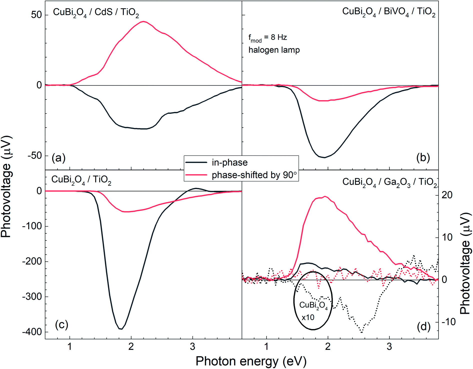 | ||
| Fig. 5 Modulated SPV spectra of the in-phase and phase-shifted by 90° signals (black and red solid lines, respectively) for the CuBi2O4/CdS/TiO2, CuBi2O4/BiVO4/TiO2, CuBi2O4/TiO2 and CuBi2O4/Ga2O3/TiO2, samples ((a)–(d), respectively). For comparison, the thin dashed black and red lines in (d) represent the measured in-phase and phase-shifted by 90° signals for a bare CuBi2O4 layer with uncontrolled surface. | ||
With regards to the phase-shifted by 90° signals, positive phase-shifted by 90° signals were found for CuBi2O4/CdS/TiO2 and CuBi2O4/Ga2O3/TiO2, suggesting that for these two samples, electrons that were separated towards the external surface were trapped in the range of the CuBi2O4/CdS or the CuBi2O4/Ga2O3 interfaces. The electron traps in the CuBi2O4/CdS interface can probably be attributed to the deep defect states seen in the amplitude spectrum of the CuBi2O4/CdS/TiO2 sample in the energy region of 1–1.5 eV. In contrast, the signs of the phase-shifted by 90° signals were negative for CuBi2O4/BiVO4/TiO2 and CuBi2O4/TiO2, i.e. holes were separated towards the external surface and trapped. This finding suggests that for these two heterojunction types, predominant trap states for holes were formed at CuBi2O4/BiVO4 and CuBi2O4/TiO2 interfaces, as shown schematically in Fig. 5b and c. Such an accumulation of trapped holes at the interface with CuBi2O4, compared to trapped electrons in the case of CuBi2O4/CdS, is much more detrimental for the PEC performance since it will lead to an increase in the total number of photogenerated electrons that will (non-radiatively) recombine. This explains the lower observed photocurrents for CuBi2O4/TiO2 heterojunction in Fig. 2a compared to CuBi2O4/CdS/TiO2.
Although in both CuBi2O4/BiVO4/TiO2 and CuBi2O4/TiO2 a combination of negative in-phase and phase-shifted by 90° signals was observed, the PEC performance of the CuBi2O4/TiO2 sample was extremely poor compared to the sample with the BiVO4 buffer layer, which requires explanation. This behavior can be attributed to an additional, pronounced difference that is observed with and without the BiVO4 buffer layer: for the CuBi2O4/TiO2 sample, in the region between 2.5–3.5 eV, the phase-shifted by 90° signal becomes larger than the in-phase signal, and the in-phase signal changes sign. Such pronounced qualitative differences can be analyzed quantitively by considering the so-called phase angle of the signal. The in-phase (x) and quadrature (y) components of the signal can be converted into the phase angle, which is defined as the arctan of the ratio between the y- and x-signals. Since the behavior of the x- and y-signals depends sensitively on transport and charge transfer processes, changes in the phase angle can provide information about changes in dominating processes in modulated charge separation. Spectra of the phase angles of CuBi2O4/CdS/TiO2, CuBi2O4/Ga2O3/TiO2, CuBi2O4/BiVO4/TiO2 and CuBi2O4/TiO2 are given in Fig. 6.
 | ||
| Fig. 6 Spectra of the phase angles of CuBi2O4/CdS/TiO2 and CuBi2O4/Ga2O3/TiO2 ((a), black squares and green stars, respectively) and of CuBi2O4/BiVO4/TiO2 and CuBi2O4/TiO2 ((b), red circles and blue triangles, respectively). | ||
For CuBi2O4/CdS/TiO2, the phase angles changed from about 140° at 1.4 eV to 119° at 2.6 eV and to 124° at photon energies above 2.85 eV. Between 2.2 and 2.6 eV, the phase angle peaked slightly from 124° to 125° at 2.4 eV (band gap of CdS), decreased to the minimum of 119° at 2.6 eV, and then increased to its saturation value after that. Therefore, since those changes were small, absorption of light by defect states near the band gap of CdS and fundamental absorption in CdS led only to little modification in trapping.
For CuBi2O4/Ga2O3/TiO2 and CuBi2O4/BiVO4/TiO2, the phase angles changed from about 75° to 86° and from about 189° to 196°, respectively. No well-defined signatures could be found within those weak changes. Therefore, deposition of Ga2O3 or BiVO4 onto CuBi2O4 does not result in the formation of additional transitions that influence the trapping dynamics.
In contrast, drastic changes were observed in the spectrum of the phase angles for CuBi2O4/TiO2. At photon energies between 1.45 and 2.15 eV, the phase angle increased from about 182° to 192°. The fact that the phase angles were so close to 180° means that the forward and backward electron transfer was the fastest at the CuBi2O4/TiO2 interface. Between 2.15 and 2.7 eV, the phase angle increased strongly to 224° which means that the electron transfer became very slow in relation to the modulation period, i.e. strong electron trapping set in. The very strong change of the phase angles up to values exceeding 270° (296° at 3.05–3.10 eV) shows that a large change in the modulated charge separation occurs at these photon energies. Specifically, a phase angle around 270° indicates that the photo-generated holes move towards the external surface and/or that the photo-generated electrons move towards the CuBi2O4/TiO2 interface. This explains the very poor performance of the CuBi2O4/TiO2 photocathode sample without a buffer layer. At photon energies 3.1 eV, the phase angle changed towards lower values (244° at 3.6 eV) giving evidence for an increased influence of the separation of electrons photo-generated in TiO2 towards the external surface. The very strong change of the phase angles for CuBi2O4/TiO2 can only be interpreted by the formation of defect states within the band gap of TiO2 near the CuBi2O4/TiO2 interface, probably caused by inter-diffusion and/or partial reduction of TiO2 by transferred and trapped holes. This notable difference in the dynamics and distribution of the charge carriers with and without the BiVO4 buffer layer, illustrated in Fig. 7b and c, demonstrates the need to prevent direct contact between the CuBi2O4 and the TiO2.
 | ||
| Fig. 7 Schematic model illustrating the distribution of charge carriers in the different heterojunctions upon illumination with white light: (a) CuBi2O4/CdS/TiO2; (b) CuBi2O4/BiVO4/TiO2; (c) CuBi2O4/TiO2 and (d) CuBi2O4/Ga2O3/TiO2. | ||
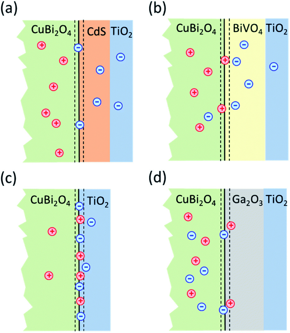
Based on the analysis of the SPV results and the correlation found with the PEC performance of the different heterojunctions, a schematic model illustrating the distribution of charge carriers in the different heterojunctions upon illumination with white light is shown in Fig. 7. The CuBi2O4/CdS/TiO2 sample (Fig. 7a) shows the highest PEC performance, which we attribute to the uniform separation of free and trapped electrons toward the TiO2 surface. When the CdS layer is replaced with BiVO4 (Fig. 7b), interfacial hole traps are formed at the CuBi2O4/BiVO4 interface, enhancing non-radiative recombination of electron–hole pairs and resulting in lower photocurrents. In the case of direct contact between the CuBi2O4 and TiO2 (Fig. 7c), large defect-related SPV signals are observed, and a large majority of the photogenerated electrons and holes are trapped at the CuBi2O4/TiO2 interface, resulting in poor PEC performance. For the case of CuBi2O4/Ga2O3/TiO2 (Fig. 7d), the charge separation efficiency is quite low compared to the other heterojunctions, probably due to the large energetic barriers due to the higher conduction band of Ga2O3 shown in Fig. 3. The charge separation direction is not favorable for photocathodic reactions, explaining the very poor PEC performance observed. Overall, based on the modulated SPV results, it can be concluded that one of the most notable differences between the different heterojunctions is the lack of trapped holes in the heterojunction containing the CdS buffer layer. Hence, we conclude that trapped holes at the interface with the CuBi2O4 are the main cause for interfacial recombination and poor photocurrents.
Conclusions
In this work, we showed that photocurrents generated from bare, unprotected CuBi2O4 photocathodes were mainly due to photo-corrosion of CuBi2O4 and not from H2 production, as claimed by many reports on Cu-based photocathodes. We investigated the influence of different buffer layers between the CuBi2O4 absorber and an n-type TiO2 film that serves as a protection layer. We found that a CdS buffer layer in combination with the ALD-deposited TiO2 protection layer and RuOx co-catalyst layer yielded a stable photoelectrode with the highest photocurrent density and faradaic efficiency for the hydrogen evolution reaction. In contrast, neither high photocurrent nor efficient hydrogen evolution was obtained for CuBi2O4/Ga2O3/TiO2, CuBi2O4/BiVO4/TiO2 and CuBi2O4/TiO2 heterojunctions. However, band alignment considerations alone cannot explain the observed trends in photoelectrochemical performance. Therefore, modulated surface photovoltage measurements were used to investigate the mechanism governing the charge transport in these heterojunctions. The modulated SPV results strongly correlated with the observed trend of the photoelectrochemical performance and revealed the formation of different interfacial states, depending on the CuBi2O4/buffer layer junction. Most importantly, it revealed which type of charge carrier was trapped at the interface with the CuBi2O4 suggesting that trapping of holes near the interface strongly limits the photo-electrochemical performance of the heterojunctions.Author contributions
The manuscript was written through contributions of all authors. All authors have given approval to the final version of the manuscript.Conflicts of interest
There are no conflicts to declare.Acknowledgements
Angang Song thanks the China Scholarship Council (file no. 201607040078) for financial support. We thank Christian Höhn for assistance with XPS and UPS measurements. We thank Lars Steinkopf for preparing CdS buffer layer and Matthias J. Müller for depositing the TiO2 protection layer by ALD.Notes and references
- S. P. Berglund, F. F. Abdi, P. Bogdanoff, A. Chemseddine, D. Friedrich and R. van de Krol, Chem. Mater., 2016, 28, 4231–4242 Search PubMed
.
- D. Kang, J. C. Hill, Y. Park and K.-S. Choi, Chem. Mater., 2016, 28, 4331–4340 Search PubMed
- R. Patil, S. Kelkar, R. Naphade and S. Ogale, J. Mater. Chem. A, 2014, 2, 3661–3668 Search PubMed
- A. Song, P. Plate, A. Chemseddine, F. Wang, F. F. Abdi, M. Wollgarten, R. van de Krol and S. P. Berglund, J. Mater. Chem. A, 2019, 7, 9183–9194 Search PubMed
- A. Song, P. Bogdanoff, A. Esau, I. Y. Ahmet, I. Levine, T. Dittrich, T. Unold, R. van de Krol and S. P. Berglund, ACS Appl. Mater. Interfaces, 2020, 12, 13959–13970 Search PubMed
- H. Gerischer, J. Electroanal. Chem. Interfacial Electrochem., 1977, 82, 133–143 Search PubMed
- S. Chen and L.-W. Wang, Chem. Mater., 2012, 24, 3659–3666 Search PubMed
- Y. Xu, J. Jian, F. Li, W. Liu, L. Jia and H. Wang, J. Mater. Chem. A, 2019, 7, 21997–22004 Search PubMed
- P. Cendula, M. T. Mayer, J. Luo and M. Grätzel, Sustainable Energy Fuels, 2019, 3, 2633–2641 Search PubMed
- Y. W. Chen, J. D. Prange, S. Dühnen, Y. Park, M. Gunji, C. E. D. Chidsey and P. C. McIntyre, Nat. Mater., 2011, 10, 539–544 Search PubMed
- B. Seger, T. Pedersen, A. B. Laursen, P. C. K. Vesborg, O. Hansen and I. Chorkendorff, J. Am. Chem. Soc., 2013, 135, 1057–1064 Search PubMed
- R. E. Brandt, M. Young, H. H. Park, A. Dameron, D. Chua, Y. S. Lee, G. Teeter, R. G. Gordon and T. Buonassisi, Appl. Phys. Lett., 2014, 105, 263901 Search PubMed
- S. Hu, M. R. Shaner, J. A. Beardslee, M. Lichterman, B. S. Brunschwig and N. S. Lewis, Science, 2014, 344, 1005 Search PubMed
- A. Paracchino, N. Mathews, T. Hisatomi, M. Stefik, S. D. Tilley and M. Grätzel, Energy Environ. Sci., 2012, 5, 8673–8681 Search PubMed
- A. Paracchino, V. Laporte, K. Sivula, M. Grätzel and E. Thimsen, Nat. Mater., 2011, 10, 456–461 Search PubMed
- S. D. Tilley, M. Schreier, J. Azevedo, M. Stefik and M. Graetzel, Adv. Funct. Mater., 2014, 24, 303–311 Search PubMed
- C. G. Morales-Guio, S. D. Tilley, H. Vrubel, M. Grätzel and X. Hu, Nat. Commun., 2014, 5, 3059 Search PubMed
- J. Luo, L. Steier, M.-K. Son, M. Schreier, M. T. Mayer and M. Grätzel, Nano Lett., 2016, 16, 1848–1857 Search PubMed
- P. Dai, W. Li, J. Xie, Y. He, J. Thorne, G. McMahon, J. Zhan and D. Wang, Angew. Chem., 2014, 53, 13493–13497 Search PubMed
- W. Cui, W. Niu, R. Wick-Joliat, T. Moehl and S. D. Tilley, Chem. Sci., 2018, 9, 6062–6067 Search PubMed
- L. Pan, J. H. Kim, M. T. Mayer, M.-K. Son, A. Ummadisingu, J. S. Lee, A. Hagfeldt, J. Luo and M. Grätzel, Nat. Catal., 2018, 1, 412–420 Search PubMed
- C. Li, T. Hisatomi, O. Watanabe, M. Nakabayashi, N. Shibata, K. Domen and J. J. Delaunay, Energy Environ. Sci., 2015, 8, 1493–1500 Search PubMed
- W. Niu, T. Moehl, W. Cui, R. Wick-Joliat, L. Zhu and S. D. Tilley, Adv. Energy Mater., 2018, 8, 1702323 Search PubMed
- W. Septina, R. R. Prabhakar, R. Wick, T. Moehl and S. D. Tilley, Chem. Mater., 2017, 29, 1735–1743 Search PubMed
- V. Duzhko, V. Y. Timoshenko, F. Koch and T. Dittrich, Phys. Rev. B, 2001, 64, 075204 Search PubMed
-
T. Dittrich and S. Fengler, Surface Photovoltage Analysis of Photoactive Materials, 2020 Search PubMed
- Y. H. Choi, K. D. Yang, D.-H. Kim, K. T. Nam and S. H. Hong, Mater. Lett., 2017, 188, 192–196 Search PubMed
- J. Lee, H. Yoon, S. Kim, S. Seo, J. Song, B. U. Choi, S. Y. Choi, H. Park, S. Ryu, J. Oh and S. Lee, Chem. Commun., 2019, 55, 12447–12450 Search PubMed
- G. Sharma, Z. Zhao, P. Sarker, B. A. Nail, J. Wang, M. N. Huda and F. E. Osterloh, J. Mater. Chem. A, 2016, 4, 2936–2942 Search PubMed
- A. Song, A. Chemseddine, I. Y. Ahmet, P. Bogdanoff, D. Friedrich, F. F. Abdi, S. P. Berglund and R. van de Krol, Chem. Mater., 2020, 32, 2408–2419 Search PubMed
- R. Gottesman, A. Song, I. Levine, M. Krause, A. T. M. N. Islam, D. Abou Ras, T. Dittrich, R. van de Krol and A. Chemseddine, Adv. Funct. Mater., 2020, 1910832 Search PubMed
- F. F. Abdi, L. Han, A. H. M. Smets, M. Zeman, B. Dam and R. van de Krol, Nat. Commun., 2013, 4, 2195 Search PubMed
- M. Butler and D. Ginley, J. Electrochem. Soc., 1978, 125, 228–232 Search PubMed
- A. Orendorz, J. Wüsten, C. Ziegler and H. Gnaser, Appl. Surf. Sci., 2005, 252, 85–88 Search PubMed
- J. M. Bolts and M. S. Wrighton, J. Phys. Chem., 1976, 80, 2641–2645 Search PubMed
- M. Mohamed, K. Irmscher, C. Janowitz, Z. Galazka, R. Manzke and R. Fornari, Appl. Phys. Lett., 2012, 101, 132106 Search PubMed
- J. Resasco, H. Zhang, N. Kornienko, N. Becknell, H. Lee, J. Guo, A. L. Briseno and P. Yang, ACS Cent. Sci., 2016, 2, 80–88 Search PubMed
- K. H. Ye, H. Li, D. Huang, S. Xiao, W. Qiu, M. Li, Y. Hu, W. Mai, H. Ji and S. Yang, Nat. Commun., 2019, 10, 3687 Search PubMed
- V. Stevanović, S. Lany, D. S. Ginley, W. Tumas and A. Zunger, Phys. Chem. Chem. Phys., 2014, 16, 3706–3714 Search PubMed
- T. Feurer, P. Reinhard, E. Avancini, B. Bissig, J. Löckinger, P. Fuchs, R. Carron, T. P. Weiss, J. Perrenoud, S. Stutterheim, S. Buecheler and A. N. Tiwari, Prog. Photovoltaics, 2017, 25, 645–667 Search PubMed
- J. Morasch, H. F. Wardenga, W. Jaegermann and A. Klein, Phys. Status Solidi A, 2016, 213, 1615–1624 Search PubMed
- P. Prajongtat and T. Dittrich, J. Phys. Chem. C, 2015, 119, 9926–9933 Search PubMed
Footnote |
| † Electronic supplementary information (ESI) available. See DOI: 10.1039/d0sc03030a |
| This journal is © The Royal Society of Chemistry 2020 |