
 Open Access Article
 This Open Access Article is licensed under a Creative Commons Attribution-Non Commercial 3.0 Unported Licence
Nitrogen-doped semiconducting oxides. Implications on photochemical, photocatalytic and electronic properties derived from EPR spectroscopy
Mario
Chiesa
,
Stefano
Livraghi
 ,
Maria Cristina
Paganini
,
Enrico
Salvadori
and
Elio
Giamello
*
,
Maria Cristina
Paganini
,
Enrico
Salvadori
and
Elio
Giamello
*
Dipartimento di Chimica, Università degli Studi di Torino, Torino, Italy. E-mail: elio.giamello@unito.it
First published on 1st July 2020
Abstract
Engineering defects in semiconducting metal oxides is a challenge that remains at the forefront of materials chemistry research. Nitrogen has emerged as one of the most attractive elements able to tune the photochemical and photocatalytic properties of semiconducting oxides, boosting visible-light harvesting and charge separation events, key elements in promoting solar driven chemical reactions. Doping with nitrogen is also a strategy suggested to obtain p-type conduction properties in oxides showing n-type features in their pristine state and to impart collective magnetic properties to the same systems. Here, we review the evolution in the understanding of the role of nitrogen doping in modifying the photochemical and electronic properties of the most common semiconducting oxides used in mentioned applications including: TiO2, ZnO, SnO2 and zirconium titanates. With an emphasis on polycrystalline materials, we highlight the unique role of Electron Paramagnetic Resonance (EPR) spectroscopy in the direct detection of open-shell N-based defects and in the definition of their structural and electronic properties. Synthetic strategies for the insertion of nitrogen defects in the various matrices are also discussed, along with the influence of the corresponding low-lying energy states on the general electronic properties of the doped solids.
1. Introduction
There is a unique parallel between aesthetics, the branch of philosophy that studies the nature of beauty, and solid state chemistry. In both cases defects, or imperfections, do not necessarily have a negative connotation, rather they are carriers of positive properties.1 Unquestionably, the point of contact between these two so different branches of knowledge is gemstones, whose distinctive charm is often due to their color. The color, in turn, is due to the presence in the crystal lattice of an extrinsic (or non-stoichiometric) point defect, i.e. a defect based on an atomic species extraneous to the composition of the solid. Traces of trivalent chromium ions, for example, impart the unique red color of ruby to the colorless crystals of corundum (a-Al2O3), making this stone a desirable gem. At the same time, however, the same defect determines the optical properties that led to the creation of the first laser.2Extrinsic defects in a solid can be either naturally occurring or deliberately introduced into the structure to generate specific properties, a procedure that goes under the name of crystal doping. Among the non-metallic elements used to dope a crystal lattice, nitrogen plays a primary role. A well-known example of nitrogen doping is that of diamond. Nitrogen is, in fact, the most common impurity found in natural diamonds, where it forms various defects that are responsible for the optical absorption and color modification of the gem. Similar to ruby, besides their gemological qualities, doped diamonds have a potential role in technology applications as they are considered the ultimate semiconductor for applications in high power electronics.3 The development of chemical vapor deposition (CVD) methods for the preparation of thin films of high purity has been accompanied by an effort aimed at introducing nitrogen into the diamond structure to obtain modified materials suitable for various applications from cold cathodes to quantum computing.4
While the study of N-impurities in diamond has been carried out for many decades, more recent research activities indicate that nitrogen is emerging as a promising doping element in many semiconducting oxides. In these solids, the valence band derives from the superposition of the fully occupied 2p orbitals belonging to the oxide (O2−) ions, whereas the empty conduction band is based on the orbitals of the metal cations. Due to the difference in energy between the atomic valence orbitals of N and O, the insertion of nitrogen in the anionic sub-lattice of the oxide causes the formation of new electronic states that usually fall inside the band gap, not far from the valence band edge. In turn, the formation of these electronic levels is fundamental for both photochemical and optoelectronic applications. In the former case, the new states modify the optical absorption and the photochemical properties of the solid. In the latter case, the electron deficient impurity – note that nitrogen has one less electron than oxygen – constitutes a shallow acceptor state potentially able to trigger the onset of p-type conductivity. Since most semiconducting oxides are n-type semiconductors, this property may be essential to engineer stable oxide-based homojunctions. A third point of interest is related to magnetism as the introduction of a nitrogen impurity in the diamagnetic oxide matrix brings about a spin magnetic moment which may in principle originate collective magnetic properties. These are highly interesting for perspective applications of semiconducting oxides in spintronics.
However, the identification and the exhaustive description of point defects in solid lattices is never an easy task. Although their presence may manifest with macroscopic effects, defects are commonly elusive species present at low, or very low, concentration. They are often only indirectly revealed on the basis of physical properties such as optical absorption, photoluminescence, electrical conductivity or Hall effect. In more than one case, however, the indirect detection has led to persistent ambiguities and controversial assignments. An almost unique tool for the description of point defects in solids is Electron Magnetic Resonance spectroscopy (EMR or EPR where P stands for Paramagnetic). This spectroscopic technique has an inherent accuracy in describing the structure and the electron spin density distribution of a given paramagnetic center, it is also remarkably sensitive allowing the detection of paramagnetic centres even at very low concentration. As an example, in one of his many seminal papers George Feher5 was able to derive the extension of the unpaired electron wavefunction around the phosphorous atom in P-doped silicon through the determination of the unpaired electron spin density by EMR: a true milestone of modern materials science. Similarly, in the case of nitrogen defects in diamond the role of the electron magnetic resonance investigations has been fundamental.6,7 As a final consideration it is to note that the obvious limitation of the technique, i.e. its inability to detect diamagnetic entities, is attenuated by the fact that numerous and extremely relevant point defects in solid materials bear unpaired electrons.8
In the present paper we intend to propose an overall survey on the main achievements obtained from the investigation of nitrogen-doped metal oxides by EPR (this more widespread acronym will be used in the following) spectroscopy. This is done on the basis of the longstanding activity of our group in the field. Over the years we have developed a comprehensive approach, in particular for each oxide we have paid attention to: (i) the nature and structure of the nitrogen defect(s), (ii) the electronic structure of the doped solid, (iii) the photochemical and optoelectronic properties induced in the oxide by the presence of nitrogen defects.
There are two main aspects in this all-round approach that have allowed a considerable insight into the nature of N-doped semiconducting oxides. Firstly, EPR gives the opportunity of recording spectra upon light irradiation under various conditions (e.g. monochromatic or polychromatic light at various frequencies between UV and near infra-red) without any direct interference between the microwave photons needed for the EPR experiment and the optical photons employed to bring the system in an excited state.9 This kind of experiments provides a direct measure of the photon energies needed to promote the electrons of the defect to the conduction band, hence on the position of the defect level into the band gap. Secondly, EPR results have always been coupled to theoretical calculations. In some cases, despite the high quality of the information acquired from the spectra, EPR measurements alone are not conclusive in establishing the nature of the crystal site hosting the defect. Therefore, comparison between the experimentally derived EPR parameters and those calculated by DFT computations may discriminate between two or more plausible models. This is possible because DFT methods have now reached a high degree of accuracy in the computation of EPR parameters, especially for the prediction of hyperfine coupling constants, which allows for reliable assignments.
This Perspective is outlined as follows. Sections 2 and 3 are devoted to short introductions to EMR spectroscopy and to a survey on the chemical methods for N doping of semiconducting oxides. Sections 4 to 7 focus on nitrogen defect centers in the most commonly used semiconducting oxides. Lastly, Section 8 proposes some general remarks on the physical properties induced by N doping in semiconducting oxides.
2. Electron paramagnetic resonance in solid state chemistry
EPR spectroscopy probes the interaction between the quantised electron magnetic moment of a paramagnetic species and an external applied magnetic field. In the most common EPR experiment the sample is irradiated by microwaves at a fixed frequency (about 9.5 GHz, or X-band frequencies) while the magnetic field is swept over a defined range. When the energy splitting between spin sublevels, induced by the applied magnetic field, matches the microwave quantum an EPR line is detected. It is to note that, although CW-EPR is an absorption spectroscopy, CW-EPR lines are commonly presented as first derivatives because the detection scheme makes use of a lock-in amplifier to enhance the signal-to-noise ratio. Although CW-EPR is the simplest of all EPR experiments it affords some unique advantages that make it a powerful research tool. Firstly, it permits a straightforward quantification, both absolute and relative, of all species detected. Secondly, it usually able to measure fast-relaxing spin species that may elude detection through pulsed EPR experiments.The EPR spectrum of a paramagnetic species can be described by the spin Hamiltonian (1) which defines the main energy terms as follows:
| H = HEZ + HHFS + HNZ + HQ + HF | (1) |
The first term is the electronic Zeeman operator (HEZ = μBS·g·B) which accounts for the interaction of the electron spin S with the external magnetic field B, μB being the Bohr magneton. The interaction is gauged by the g tensor, a 3 × 3 matrix which, in general, can be reduced to its diagonal form. The principal elements of the diagonal g matrix gxx, gyy, gzz assume values which depend on the electronic structure (ground and excited states) of the paramagnetic species and can be interpreted as the analog of the NMR chemical shift.
The second term (HHFS = S·A·I) is much more important in our case because it represents the hyperfine interaction between electron spin and nuclear spins. A is the hyperfine tensor and I is the nuclear spin vector. In CW-EPR the hyperfine interactions give rise to lines splitting in the spectrum (the hyperfine structure). 2I +1 lines are expected for the interaction of the electron spin with a nucleus having nuclear spin quantum number I. A is composed of two main contributions, i.e. the isotropic Fermi contact term (a scalar arising from the finite probability of the electron being located at the position of the nucleus) and the anisotropic electron-nucleus dipolar coupling expressed by a matrix T. From the analysis of the hyperfine interaction, the local symmetry and the degree of spin delocalization and the nature of the chemical bond can be recovered, with high accuracy.
The third and fourth terms in eqn (1) – representing the nuclear Zeeman energy and the nuclear quadrupolar energy respectively – do not usually affect standard CW-EPR spectra, but play an important role in so called hyperfine techniques (ENDOR, ESEEM), providing important information on the identity of the nucleus coupled to the electron spin and the electric charge distribution around it. The last term, known as the fine structure term (HF = S·D·S) describes the interaction between two or more unpaired electrons through the D tensor. This term is zero in the case of S = 1/2 and will not be taken into account in the following discussion as the majority of defects encountered in nitrogen doped semiconducting oxides and photo-generated electron and holes pairs are characterized by S = 1/2.
All magnetic interactions strongly depend on the relative orientation between the paramagnet and the applied magnetic field, and are therefore said to be anisotropic. This is to say that if the unpaired electron occupies a p orbital, as in the case of a N defect, the interaction energy will be different if the axis of the orbital is parallel or perpendicular to applied magnetic field. This is exemplified in Fig. 1, where the singe crystal and powder spectra of a single nitrogen impurity are simulated.
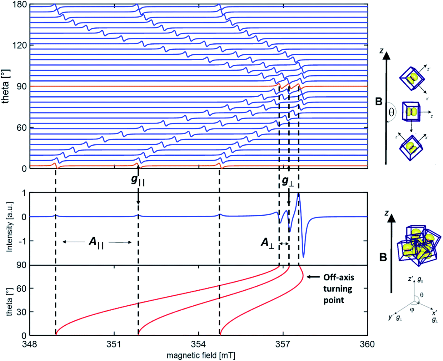 | ||
| Fig. 1 Simulated single crystal (upper panel) and powder (lower panel) EPR spectra of a nitrogen impurity. The red spectra in the single crystal road map correspond to the parallel (θ = 0°) and perpendicular (θ = 90°) orientations of the radical axes with respect to the external magnetic field. The dotted lines indicate the hyperfine transitions corresponding to the parallel and perpendicular orientations. The g and A tensor axes have been assumed to be coincident. The anomalous intensity of the high field transition in the powder spectrum is due to the presence of an off-axis turning point evidenced in the figure (see text for an explanation). | ||
The anisotropy of the magnetic tensors implies that, in the case of a single crystal (upper panel in Fig. 1), the EPR signal changes according to the orientation of the crystal in the external magnetic field. EPR spectra are usually recorded, in this case, at various orientations rotating the crystal about each reference axis and obtaining distinct curves of g and A values as a function of the rotation angle. The curves are than fitted with the theoretical formulas by adjusting the relevant parameters, i.e. the g and A values, which are thus obtained with a high degree of accuracy.
Polycrystalline materials (or powders) are disordered systems composed of many small crystallites randomly oriented in space. In this case one single spectrum, called a “powder spectrum” (lower panel in Fig. 1), is recorded which is an envelope of signals corresponding to all possible orientations of the paramagnetic species in the magnetic field. In a randomly oriented sample the number of features in the EPR spectrum is determined by the following condition:
| ∂B/∂θ = 0 and ∂B/∂ϕ = 0 | (2) |
The three solutions, where θ = 0 (Bz), θ = π/2 and ϕ = 0 (Bx), θ = π/2 and ϕ = π/2 (By), correspond to the usual principal components observed in the singe crystal spectrum. Since θ and ϕ are in the g-matrix axis system, observable features are expected for those fields corresponding to orientations along the principal axes of the g matrix. This being the case, the principal values of the g-matrix are obtained. In the case at hand (i.e. a nitrogen impurity) for each principal direction of the g tensor the signal is additionally split into 2I + 1 = 3 lines due to the hyperfine interaction of the unpaired electron with the 14N nucleus (I = 1). Powder spectra with hyperfine structure can thus be interpreted in term of spectral features identified with orientation of the magnetic field along one of the g and hyperfine matrix principal axes. In some circumstances, due to specific ratios between the g and A tensors anisotropy, extra lines, non-coinciding with the principal axes orientations may appear in the powder spectrum. Such extra lines known as off-axes turning points can have considerable intensity, as shown in the powder spectrum of Fig. 1, where such a feature corresponds to a solution of eqn (2) for θ ≈ 74°. In such cases the spectra may become very complex and the intrinsically lower accuracy in the determination of the spin-Hamiltonian parameters can be attenuated adopting particular procedures such as the use of suitable isotopic substitutions and multifrequency approaches.
In the study of nitrogen impurities, 14N (I = 1) can be substituted by the 15N isotope (I = 1/2). This causes predictable changes in the measured EPR spectra that reflect in both the number and spacing of the resonance lines, helping the interpretation by comparison of the two spectra. Both the isotropic and anisotropic hyperfine interaction depend on the nuclear g factor, therefore substitution of one isotope (gN) with another (gN′) causes a change of the coupling constant proportional to the ratio gN′/gN. For instance, substituting 14N (gN = 0.4038) with 15N (gN′ = −0.5664) causes an increase of the measured hyperfine constant by a factor −1.4027. Moreover, the number of hyperfine lines, determined by the rule 2I + 1, decreases from three to two in the example.
Another important experimental tool is provided by the multifrequency approach. Recording the EPR spectrum at a higher frequency (e.g. 35 GHz, Q band) leads to an increase in the separation between the various g components while the hyperfine splitting remains fixed. This, combined to isotopic substitution, allows a better understanding of the structure of congested spectra. Finally, the systematic use of computer simulation of the experimental spectra is essential to verify the goodness of the assignments and to fine tune the determination of the spin-Hamiltonian parameters. For a wider introduction to the applications of EPR to the study of defects in the solid state the reader is referred to the book by Spaeth and Overhof.10
3. Chemical routes for N doping of oxides
In order to introduce nitrogen defects in metal oxides several procedures are reported in the literature that include: (i) wet chemistry methods; (ii) thermochemical treatments of bare oxides; (iii) typical methods of solid state chemistry such as Chemical Vapour Reaction or Transport (CVR, CVT); and (iv) physical methods such as ion implantation, magnetron sputtering and so on.Wet chemistry methods are characterized by mild reaction conditions and usually involve the crystallisation of the desired oxidic matrix in the presence of a suitable nitrogen source. The final step of the preparation is usually a thermal treatment performed with a twofold goal: (i) the formation of well crystallized solids; and (ii) the decomposition of the nitrogen source with simultaneous incorporation of nitrogen into the solid matrix. Polycrystalline materials are readily prepared in this way, however the same procedures can be easily oriented to the obtainment of thin films using specific strategies such as deep coating or spin coating methods. Metal alkoxides and soluble salts precursors are usually employed in wet chemistry preparations while, in the case of reactants with low solubility, hydrothermal or solvothermal methodologies can be successfully employed to overcome the drawback.
On the other hand, the direct treatment of a preformed bare oxides requires vigorous treatments since the lattice energy of the solid has to be exceeded. The needed activation energy can be provided by various methods for instance conventional thermal treatments, plasma treatments, ball milling (mechanochemistry), that are normally carried out in the presence of a reactant which acts as nitrogen source. Such a preparation strategy has the advantage of being applied directly on materials in the form of thin film or single crystals an guarantees greater control over the morphology of the final nitrogen doped solids. However, since the process of nitrogen incorporation originates from the surface, a gradient of the nitrogen impurity concentration may occur.
Finally, physical methods for doping require, in most cases, complex and expensive apparatuses. These methods are preferentially employed to prepare thin films. The well-defined and constant experimental conditions allow a strict control of the nitrogen content minimizing the formation of byproducts. Table 1 summarizes the main features of the synthetic approaches described in this section.
| Material | Preparation method | Oxide precursor | N source | XPS (eV) | |
|---|---|---|---|---|---|
| N–TiO2 | Wet chemistry | Sol–gel | Metal alkoxides, TiCl4 | NH4+ salts, urea, NH3, aliphatic amines | ∼397 to ∼400 |
| Hydrothermal or solvothermal | Metal alkoxides, TiN | NH3, amines | ∼397 to ∼400 | ||
| Ti-containing salt | |||||
| Precipitation | Ti-containing salt | NH3 | ∼400 | ||
| Chemical treatment | Ball milling | TiO2 | NH3 | ∼397 to ∼400 | |
| Nitration at high temperature | TiO2 | NH3, NOx | ∼397 to ∼400 | ||
| TiN oxidation | TiN | — | ∼397 | ||
| Physical techniques | Magnetron sputtering | TiO2 | Atomic N | ∼397 to ∼400 | |
| Ion implantation | TiO2 | Atomic N | ∼397 | ||
| CVR | Metal alkoxides, TiCl4 | N2, urea, NH3 | ∼397 to ∼400 | ||
| N–SnO2 | Wet chemistry | Precipitation | SnCl2, SnCl4, metallic Sn | NH3 | ∼397 to ∼400 |
| Chemical treatment | Nitration | SnO2 | N2, NH3 | ∼397 to ∼400 | |
| Physical techniques | Magnetron sputtering | SnO2 | Atomic N | ∼397 | |
| N–ZnO | Wet chemistry | Impregnation | ZnO | (NH4)CO3 | — |
| Physical techniques | CVD | Metal alkoxides | N2, NH3 | ∼397 to ∼400 | |
| Ion implantation | ZnO | Atomic N | ∼397 to ∼400 | ||
| Chemical treatment | Nitration at high temperature | ZnO | N2, NH3 | ∼397 to ∼400 | |
| N–ZrTiO4 | Wet chemistry | Sol–gel | TTIP/ZrOCl2 | NH4Cl | — |
The enormous interest in nitrogen doped TiO2 due to its application as visible-light-active (VLA) photocatalyst has produced a huge number of preparation procedures that are available in the literature. In this context wet chemistry methods such as sol–gel11,12 and hydrothermal syntheses13,14 prevail. Nevertheless, several examples involving treatments of bare TiO2 (ball milling,15,16 annealing in reacting atmosphere17,18) as well as more sophisticated solid state chemistry (CVR)19 or physical methods (ion implantation,20,21 magnetron sputtering22,23) are also reported. As it will be illustrated, wet chemistry methods preferentially lead to the interstitial forms of N defects (NO2−˙, NO3−) whereas the methods involving high temperature treatments (nitridation) in reactive atmosphere usually lead to nitrogen impurities in substitutional position. These two forms of nitrogen impurity are usually discriminated on the basis of the corresponding N 1s XPS peak, at about 396–397 eV for the substitutional one and around 400 eV for the interstitial.24 Several other chemical species however, not related to bulk N defects show XPS peaks in the range 398–400 eV causing some ambiguity in the interpretation of XPS results. A survey on the preparation methods, the reagents employed, the resulting crystalline structure and the type of N defect formed is provided in Table 2.
| Material | Preparation method | Oxide precursor | N precursor | Crystalline structure | N impurity | XPS (eV) | Ref. |
|---|---|---|---|---|---|---|---|
| a TTIP = titanium tetraisopropoxide, TE = titanium ethoxide. A = anatase, R = rutile, W = wurtzite, S = scrutinyite. Ni = interstitial nitrogen, Ns = substitutional nitrogen. | |||||||
| N–TiO2 | Sol–gel | TTIP | NH4Cl | A | Ni | 400 | 37 |
| N–TiO2 | Sol–gel | TTIP | NH4Cl | R | Ni | — | 39 |
| N–TiO2 | CVR | TE | Urea | A | Ni | — | 46 |
| N–TiO2 | Hydrothermal | TTIP | NH3 | A | Ni | — | 25 |
| N–TiO2 | Ball milling | TiO2 | NH4Cl | A + R | Ni | 400 | 43 |
| N–TiO2 | TiN oxidation | TiN | — | R | Ni | 400 | 43 |
| N–TiO2 | N2 plasma | TiO2 | N2 | A | Ni | 400 | 42 |
| N–B–TiO2 | Sol–gel | TIPP | NH3/H3BO3 | A | Ni | — | 59 |
| N–F–TiO2 | Sol–gel | TIPP | NH4F | A | Ni | — | 55 |
| N–SnO2 | Precipitation | Sn or SnCl4 | NH3 | R | Ns | 397–400 | 90 |
| N–ZnO | Nitration | ZnO | NH3 | W | Ni (N2−) + Ns | — | 79 |
| N–ZrTiO4 | Sol–gel | TTIP/ZrOCl2 | NH4Cl | S | Ni | — | 93 |
4. N doping of titanium dioxide
Titanium dioxide (TiO2) is the most investigated binary metal semiconducting oxide because it has found application as a functional material in areas connected to sustainable energy, environment and health. Just as a partial series of examples one can mention the activities in the fields of artificial photosynthesis,26 photocatalysis for pollutant abatement,27 photovoltaics as a substrate in dye sensitized solar cells28 and biocide systems.29 In all these areas the photophysical properties of the solid along with its surface structure30 and surface reactivity31 play an utmost role.Titanium dioxide exists in three main polymorphs, namely anatase, rutile, brookite, whose structures are all based on TiO6 distorted octahedra connected by trigonal coordinated oxygen ions (OTi3). The band gap value ranges between 3.0 eV and 3.2 eV depending on the polymorph. TiO2 is a n-type semiconducting oxide owing to tiny oxygen deficiencies with respect to the stoichiometric ratio entailing the formation of shallow donor states whose electrons are easily excited in the conduction band. Since the band gap value of the various polymorphs requires the use of UV frequencies for electron photoexcitation, the attempts of doping this oxide with nitrogen were in fact originally performed with the aim of obtaining a VLA system, a requirement for most photochemical and photocatalytic applications. Preparation of efficient visible-light-active systems is, in fact, the necessary condition for the use of sun light in large scale photocatalytic plants.
The first report on nitrogen doped anatase (hereafter N–TiO2) dates back to 1986,32 but it is only at the beginning of the XXI century that the attention of researchers was strongly attracted by this system due to both its capability of absorbing visible light (an absorption band with maximum around 440 nm overlaps with the band gap transition at 390 nm producing the yellow color of the solid) and to some promising results in photocatalytic experiments under visible light.33 The huge number of studies that rapidly appeared, were based on different approaches to prepare this novel systems, mainly by wet chemistry methods (see Section 3) but also by physical methods such as magnetron sputtering or by high temperature treatments with nitridation agents in gas phase.34 This intense experimental activity generated a high number of scattered results and interpretations concerning the origin of N–TiO2 photochemistry under visible light. Review papers summarizing the bulk of experimental results about both nitrogen doped oxides in photocatalysis35 and N–TiO2 in particular have already appeared.36 In this Perspective we will restrict ourselves to the description of the impact of EPR in this field of research.
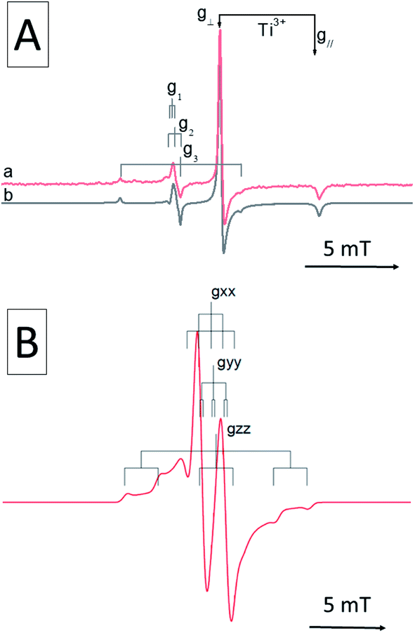
The classic CW-EPR technique gave a major contribution to define the nature and features of the N-based photoactive center. It was in fact shown that, in the case of materials prepared by wet chemistry, nitrogen paramagnetic centers form in the bulk of both anatase and rutile polymorphs.37 One of these, in particular, plays a decisive role in the photochemistry of the system under visible light. This previously unreported species is characterized by a simple EPR signal indicating the presence of one nitrogen atom only (Fig. 2). The signal in fact is characterized by a hyperfine triplet indicating that the unpaired electron interacts with a single nucleus of 14N (nuclear spin I = 3/2, expected lines 2I + 1 = 3). A further proof of the monoatomic nature of the new species was attained using 15N (I = 1/2) containing reactants in the preparation and observing a hyperfine doublet as expected.38 The g tensor of the N species is poorly informative with the three principal values close one another. On the other hand, the hyperfine interactions, fully determined by computer simulation of the experimental lines, shows a larger coupling in one direction and smaller ones in the other two directions. Despite the structural difference between the TiO2 polymorphs, the EPR spectra and the corresponding spin-Hamiltonian parameters are very similar, though not identical (Table 3), firmly indicating that the N centers formed in anatase and in rutile are substantially alike.
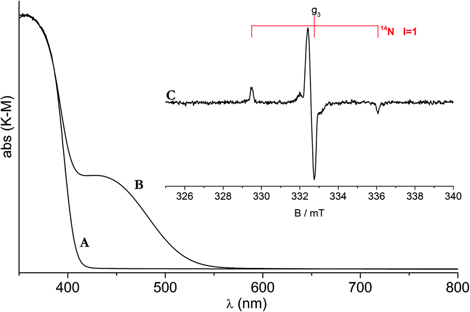 | ||
| Fig. 2 UV-Vis and EPR spectra of N-doped rutile TiO2. Optical absorption of pristine (A) and N-doped rutile (B). (C) EPR spectrum of N doped rutile. | ||
| System | Species | g 1 | g 2 | g 3 | A 1/mT | A 2/mT | A 3/mT | Spin density in N(2s), ρN(2s) | Spin density in N(2p), ρN(2p) | Ref. |
|---|---|---|---|---|---|---|---|---|---|---|
| N–TiO2 A | NO2−˙ | 2.007 | 2.005 | 2.004 | 0.23 | 0.44 | 3.23 | 0.02 | 0.54 | 38 |
| N–TiO2 R | NO2−˙ | 2.005 | 2.004 | 2.003 | 0.06 | 0.44 | 3.28 | 0.02 | 0.57 | 39 |
| TiO2 A single crystal | N | 2.0064 | 2.0056 | 2.0038 | 0.226 | 0.360 | 3.179 | 44 | ||
| N–W co-doped, A | [NiO]W | 2.002 | 2.001 | 2.000 | 0.8 | 0.8 | 5.0 | 0.035 | 0.707 | 57 |
| N–B co-doped, A | [NOB]˙ | 2.004 | 2.003 | 2.001 | 0.93 | 0.99 | 5.04 | 0.03 | 0.70 | 59 |
4.1 N centers in TiO2. Composition and structure
The nature and the structural features of the nitrogen containing species were unraveled by coupling EPR and DFT calculations. EPR in fact allows to evaluate the electron spin density on the nitrogen atom (Table 3). In both anatase and rutile,39 the detected spin density is essentially confined in a 2p orbital of nitrogen (hyperfine dipolar interaction) with a minor contribution of 2s orbital (Fermi contact term), essentially due to spin polarization. It is evident however that the spin density detected by EPR amounts to 0.56–0.59 of the total, so that about 40% of it escapes detection.The computational analysis considered two possible models for the paramagnetic nitrogen center: “substitutional”, with a N ion taking the position of a O ion in the oxide lattice and “interstitial” with N that occupies a cavity of the TiO2 structure. Although the calculated spin density on N is not radically different in the two cases the second model, “interstitial N”, shows a better fit with the experiment in terms of both spin density and position in the band gap (about 0.7 eV over the VB edge, see below). In this model (Fig. 3) the N atom is not symmetrically located into the lattice interstitial space but, rather, it is close to a specific O ion with which it forms a true covalent bond.
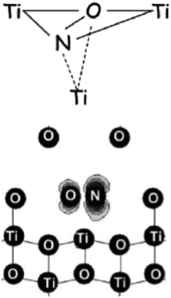 | ||
| Fig. 3 Two different pictorial views of the N interstitial center in TiO2. In the lower sketch the computed electron spin density is also visible (figure adapted from ref. 12). | ||
The fraction of the spin density missing in the experimental EPR spectrum is thus on the oxygen of the charged NO moiety as shown in Fig. 3. This cannot be directly assessed due to the very low natural abundance of the only magnetically active isotopes of oxygen (17O, I = 5/2, ab. 0.037%), but can be estimated by difference.
This model was confirmed by successive works, at least for all the polycrystalline N–TiO2 systems prepared via wet-chemistry methods (see below). Substitutional N, at variance, forms when TiO2 is submitted to high temperature treatments in ammonia (nitridation) as suggested by XPS.
TiO2 systems with small concentrations of substitutional nitrogen are less active in photocatalytic reactions than those containing interstitial impurities and, for this reason, are less investigated. Substitutional N is present in TiO2 submitted to nitridation or, alternatively, in oxidized titanium nitride (Ti3N4). In the latter case the resulting material is compound with intermediate stoichiometry between TiO2 and Ti3N4. However extended nitridation of some oxides lead to the obtainment of compounds called oxynitrides, which show significant photocatalytic activity in water photosplitting.40 This is still a completely different class of compounds which displays various stoichiometry and have been discussed in a thorough review paper devoted to anion modified oxides in heterogeneous catalysis41 and, for these reasons, are not considered further here.
A conclusive evidence on the features of the interstitial N center in TiO2 was derived by a crucial clear-cut experiment performed by our group.42 Several contradictory messages were in fact present in the literature concerning the nature and the location of N photoactive species in TiO2. This happened because a variety of synthetic approaches and nitrogen sources have been used to prepare the doped materials (ammonia, ammonium salts, amines, urea etc.). Each synthetic method may form several byproducts (ammonium ions, cyanides, aliphatic groups etc.) which locate mainly, but not exclusively, at the surface of the solid and generate ambiguities in the individuation of the true photoactive species.43 The ambiguity stems also from the fact that several nitrogen containing species have the same XPS binding energy around 400 eV (N 1s) which coincides with the value assigned to the interstitial nitrogen species (see Section 3 and Table 1). In the mentioned experiment,42 a sample of pure anatase was kept under N2 atmosphere in a liquid nitrogen bath while a plasma glove discharge generated free N atoms in the gas phase. These are reactive enough to penetrate in the solid material kept at low temperature and form the same interstitial photoactive species also observed in samples prepared via sol–gel. This was confirmed by EPR and XPS spectroscopies which yielded the same features and spectral parameters in the two cases. It is to note that crucially under the experimental conditions described a substitution of lattice oxygen by N atoms is simply impossible.
To conclude, nitrogen forms a main impurity center in sol–gel TiO2. Such species is based on the formation of a chemical bond between nitrogen and a lattice oxygen ion. Since the latter is formally an O2− ion the stoichiometry of the photoactive center is NO2−˙, a 13-electron radical species. Due to covalent contributions, the charge on both the lattice oxygen and the N species is actually lower than −2. The impurity center has a well-defined EPR signal and spin density shared by N and O and the surrounding lattice (Fig. 3). The SOMO of this unprecedented chemical species is a π antibonding orbital involving 2p atomic orbitals of N and O respectively.
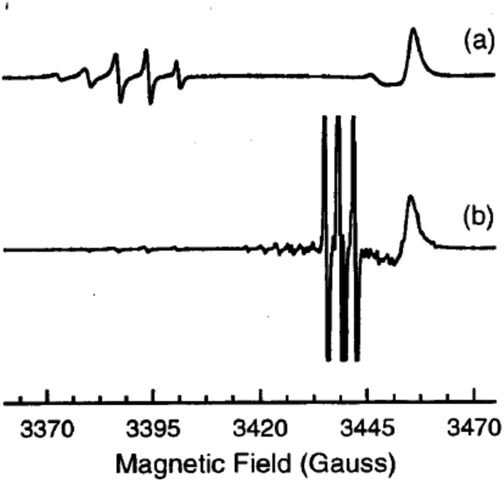
As a point of reference, only one example is available in the literature reporting EPR spectra of N–TiO2 in a single crystal. In their paper T. Sekiya et al.44 report careful measurements on a crystal obtained by CVT in the presence of NH4Cl (Fig. 4). The parameters reported by these authors are collected in Table 3 and result very close to those previously measured by some of us38,39 in the case of polycrystalline powders, thus providing a further validation to these results.
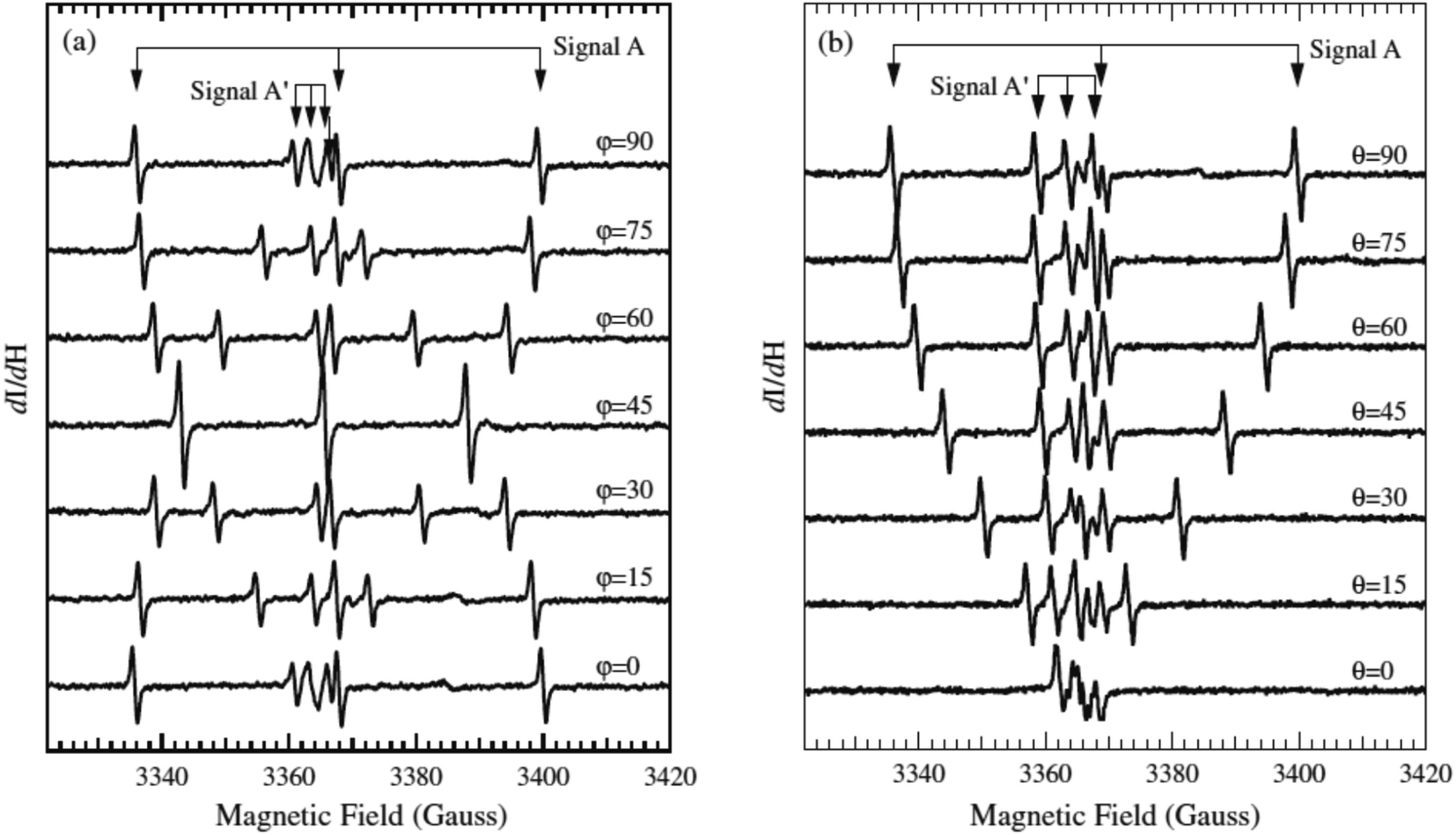 | ||
| Fig. 4 EPR spectra of a single crystal of N–TiO2 recorded as a function of the orientation. ϕ and θ are the angles of the external magnetic field H with two axes of the crystal ((a) and (b) respectively). Magnetic field is in gauss (1 G = 0.1 mT). Figure reproduced with permission from ref. 44. | ||
The authors suggest that the paramagnetic nitrogen substitutes oxygen in the lattice, but do not exclude that it could occupy an interstitial site of the lattice. In both cases, in fact, the unpaired electron is mainly confined in a 2p N orbital and the angular dependence of the tensors would be the same. However, on the basis of the similarity of the hyperfine parameters (small electron 2p(N) spin density) and of the DFT calculations discussed above, we confidently infer that the NO2−˙ observed in powdered materials is responsible for the spectra recorded by Sekiya in the single crystal system.
4.2 Photosensitivity of N centers in TiO2
To demonstrate the photoactivity of the observed N species, EPR spectra were recorded under irradiation. It was shown that using a monochromatic wavelength of about 440 nm (corresponding to the maximum of optical absorption in the blue at an energy of 2.8 eV) the intensity of the EPR signal increases.45 The same does not occur at other visible wavelengths away from the absorption maximum confirming two crucial facts: that (i) both the absorption in the visible and the described EPR signal are due to interstitial nitrogen species; and (ii) the latter is an intra band gap state, approximately placed at 0.4 eV above the valence band.Light at 440 nm – that is ineffective on pristine TiO2, band gap energy Eg = 3.2 eV – excites electrons from the intra band gap state associated with the interstitial nitrogen impurity to the conduction band. Remarkably, since the effect of visible light excitation is a net increase of the intensity of the EPR signal, the operating mechanism at the origin of such phenomenon must involve the presence of a diamagnetic partner of NO2−˙ bearing one additional electron and having similar electronic energy. In other words, the observed effect reveals the presence of an EPR silent species, formally NO3−, beside NO2−˙. The two species are related by eqn (3):
| NO3−(↑↓) + hν(vis.) → NO2−˙ (↑) + e−(CB) | (3) |
When the excitation is turned off, recombination occurs through the reverse process.
The increase of paramagnetic NO2−˙ centres upon selective irradiation implies that NO3− diamagnetic centres are more abundant and are therefore preferentially affected by selective irradiation. The same experiment performed under O2 atmosphere leads, beside the increase of the NO2−˙ signal intensity, to the formation of surface adsorbed superoxide ions (O2−˙) which are also paramagnetic and exhibit a typical EPR signal (Fig. 5). This occurs according to the following, irreversible, process
| NO3− + O2 + hν(vis.) → NO2−˙ + O2−˙(surf) | (4) |
 | ||
| Fig. 5 EPR spectra (left) of N–TiO2 in the dark and after irradiation with blue light. Top spectrum: overlap between the signals of NO2−˙ (with increased intensity) and superoxide (see eqn (4)). Schematic picture (right) describing the intra-band gap states in N–TiO2 and the photoexcitation mechanism. | ||
Several others papers have reported EPR spectra of N–TiO2 powders. In most cases these were supporting results that did not provide further insight into the features of the photoactive species. We note however that the spectral parameters derived in those studies47–52 were consistent with those already discussed.
A remarkable exception is a paper by D'Arienzo et al.53 reporting a careful analysis of the photonic efficiency of N–TiO2 (anatase). This was done by measuring the increment of photonic absorption due to the presence of nitrogen defects in the system and comparing this value with the detrimental effect, in term of recombination of UV-generated charge carriers, ascribable to the same centers. This type of approach is extremely useful for the selection of the appropriate wavelength to be employed in photocatalytic applications.
4.3. Other N containing defects in TiO2
After the discovery of N–TiO2 a great deal of work was performed to increase the visible light absorption of titanium dioxide. A popular strategy was the simultaneous insertion of another elements in the crystalline structure beside nitrogen. In most cases the result was the production of co-doped materials with the two elements segregated in distinct sites of the solid, such as in the case of fluorine-nitrogen co-doped titania.54 The EPR spectrum of a N–F–TiO2 displays the typical signal of the NO2−˙ species55 (identical, though usually less intense, to that of same observed in N–TiO2) as well as that of Ti3+ (Fig. 6, top). The two signals fall in different regions of the spectrum and are only partially overlapped. The formation of Ti3+ is due to the insertion of F in the lattice56 as fluorine bears an extra electron with respect to oxygen (n-type dopant) that is scavenged by Ti4+ ions. The relevant effect observed in this material is the charge compensation due to the simultaneous presence of a p-type (N) and an n-type (F) dopant causing an internal partial charge transfer, according to the equilibrium in eqn (5), from the high lying Ti3+ 3d states to the low lying N states with an overall stabilizing effect.| Ti3+ + NO2−˙ ↔ Ti4+ + NO3− | (5) |
 | ||
| Fig. 6 EPR spectra of N–F doped anatase TiO2 (A) with the signals of the two independent centers (NO2−˙ and Ti3+) and (B) EPR spectrum recorded in N–W co-doped material showing a center containing interacting N and W dopants. This part of the figure is adapted with permission from ref. 57. | ||
This reduces the energy cost needed to dope the material and allows to reach a higher level of nitrogen doping with respect to the parent N–TiO2 system. The EPR spectrum reveals no evidence of interaction between N and F impurities, suggesting that the doping occurs independently in different regions of the crystal.
On the other hand, Folli et al.57 reported the co-doping of tungsten and nitrogen in the TiO2 matrix (N–W–TiO2). In this case EPR showed the presence of novel nitrogen species, beside the usual NO2−˙ signal. The novel paramagnetic centres are still based on a single interstitial nitrogen, as shown by the typical three-line pattern. However, due to a significant interaction with a tungsten ion, the g tensor elements are shifted at lower values. Moreover, the N hyperfine tensor components are larger as compared to NO2−˙, indicating a higher electron spin density on the N atom of the defect (Table 3). In one case even a superhyperfine interaction due to a 183W (I = 1/2) nucleus was also observed (Fig. 6, bottom).
Another unprecedented extrinsic defect in anatase TiO2 was reported for a nitrogen and boron co-doped materials (N–B–TiO2). Similar to N–W–TiO2 (Fig. 6 bottom), this center involves both N and B atoms and was first synthetized by Ke and coworkers58 in order to indirectly monitor the nature of the active centers in singly doped B–TiO2, using nitrogen as a convenient probe for EPR investigations. Later, the nature of this novel paramagnetic defect was tackled by coupling EPR and DFT calculations. N–B–TiO2 shows a complex EPR spectrum, as reported in Fig. 7.59 The spectrum of the typical NO2−˙ center in anatase corresponds to the three narrow lines separated of 3.23 mT (Fig. 7A, obtained using 14N) and to the narrow doublet (Fig. 7B, 15N) with a larger splitting of 4.55 mT, as expected the ratio between the nuclear g factor of the two nuclei. The N–B center shows again a 14N triplet and a 15N doublet of lines having higher hyperfine separation than NO2−˙ due to a larger electron spin density on the N-2p orbital (Table 3). Each line is however modulated in a quartet of lines (see stick diagrams in Fig. 7) due to a further interaction of the unpaired electron with a single boron nucleus. The most abundant boron isotope (11B) has in fact nuclear spin I = 3/2 (2I + 1 = 4 lines expected) and 80% natural abundance. To pinpoint the exact structure of this defect, several structural models have been tested by DFT calculations. One case only provided an excellent agreement between predicted and experimentally derived EPR parameters. The model of this novel centre is based on the bonding of both N and B to the same lattice oxygen with the B atom further linked to two other nearby oxygens, a schematic for this structure is reported in Fig. 7. The electron spin density derived from EPR and DFT is unevenly distributed between N (0.7) and B (0.07), but in both cases resides on the 2p orbitals. Again, due to the lack of non-zero nuclear spin isotopes of oxygen, the experimental value of the spin density on oxygen(s) remains unknown.
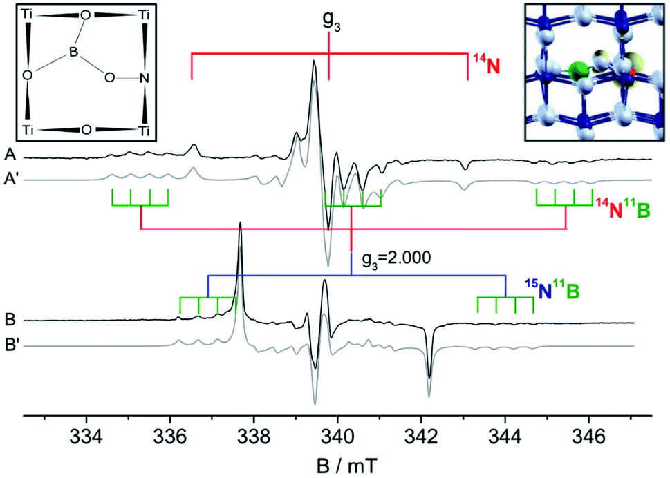 | ||
| Fig. 7 EPR spectra (and related computer simulation, dash-dotted trace) of N–B co-doped titanium dioxide. Spectrum (A) was obtained using reactants with nitrogen in natural abundance (99.6% 14N, I = 1), spectrum (B) using reactants enriched in 15N, I = 1/2 (100%). In the inset two graphic sketches of the B–N center. Nitrogen, red; boron, green; oxygen, gray. In yellow the computed electron spin density. | ||
5. N doping of zinc oxide
Zinc oxide (ZnO) is a semiconducting oxide with n-type character due to the presence of shallow donor impurities including hydrogen.60 ZnO has a direct band gap around 3.4 eV and shows the typical structure of wurtzite, with both zinc and oxygen in tetrahedral coordination and a non-negligible degree of covalency between cations and anions.61 Similar to other semiconducting oxides, the synthesis of a p-type variety of ZnO might open a series of highly interesting applications in optoelectronics, such as light emitting devices and laser diodes.62 A p-type behaviour has been reported in the case of N–ZnO films prepared by annealing of sputtered oxynitride films63 or by magnetron sputtering,64 even though these electronic properties seems to be unstable and decline over time.65,66 On the basis of theoretical forecasts, N–ZnO based structures have also been considered as dilute magnetic semiconductors showing ferromagnetic interactions among nitrogen centers67,68 and experimental observation of such a behaviour have already been reported in the literature.69Various techniques have been used to introduce nitrogen into the ZnO matrix, depending on the morphology of the bare system nitrogen has been successfully introduced in ZnO single crystals grown through a chemical vapor deposition process and successively annealed in a N2 flow at high temperature (see below). ZnO nanorods have been produced on fluorine tin oxide substrates and nitrogen has been introduced via ion implantation technique.70 Thin films were grown by plasma-assisted molecular beam epitaxy on c-plane sapphire substrates and N impurities were deposited on the anion site by ion implantation.71 In parallel, the synthesis of nanostructured polycrystalline N–ZnO materials has also been described72 whose interest, like in the case of N–TiO2, is related to the search for photoactive systems working in visible light in particular for the water splitting reaction.73 Polycrystalline ZnO have been doped following classic wet chemistry process using a solution of ammonium carbonate followed by an annealing at 750 °C. In various other cases N–ZnO has been obtained starting from commercial ZnO nanosized powders heated in NH3 gas.74
Clearly, N–ZnO is of great practical interest and it has been subject to extensive EPR investigations, both in single crystal and polycrystalline forms.
5.1 Nitrogen impurities in ZnO single crystals
In 2001, W. E. Carlos et al. reported the first EPR spectra recorded at 4 K of a N impurity serendipitously formed in single crystals of ZnO either annealed at high temperature or irradiated by an electron beam.75 The spectra, recorded in the dark, show the symmetric triplet expected for a paramagnetic centre coupled to a single N atom. The angular dependence of the EPR signal indicates an axial symmetry for both g and A tensors (Table 4), which is indicative of a singly occupied molecular orbital (SOMO) with almost pure p character (96%). On the other hand, from the hyperfine coupling it can be inferred that only 45% of the electron spin density is localized on the N atom. The Halliburton group reported comparable results for single crystals of ZnO treated in air or in nitrogen between 873 K and 1273 K. Those crystals are EPR silent in the dark but become EPR active upon irradiation at wavelengths between 364 nm and 514 nm.76 The EPR signal was assigned to neutral paramagnetic acceptor states N0. These forms from N− diamagnetic states which are light converted to N0. This behaviour is reminiscent of what described in the case of N–TiO2 in Section 4.2. A steady-state signal due to N0 is observed at 6.5 K under continuous illumination which, once irradiation is removed, disappears through recombination within several hours. Also in this case the angular dependence of the signal indicates that the both g and A tensor of the N0 centre have axial symmetry (Table 4).| Sample | Centre | g tensor | A/MHz | A/mT | Ref. | ||||
|---|---|---|---|---|---|---|---|---|---|
| g ∥ | g ⊥ | A ∥ | A ⊥ | A ∥ | A ⊥ | ||||
| Single crystal | N | 1.9953 | 1.9633 | 2.953 | 0.361 | 75 | |||
| Single crystal annealed in N2 | N0 | 1.9948 | 1.9632 | 81.3 | 9.5 | 2.90 | 0.34 | 76 | |
| Nanopowders annealed in NH3 at 773 K | N2− | Exp. | 1.9947 | 1.9630 | 81.3 | 8.6 | 2.90 | 0.31 | 79 |
| N2− subst. | Theory | 82.1 | 11.4 | 2.93 | 0.40 | ||||
| Single crystal by seeded CVT in N2 stream | N2− | 2.0036 | 1.9935 | 9.8 | 20.1 | 0.35 | 0.72 | 77 | |
A short time later the same group investigated a ZnO single crystals grown by the seeded chemical vapour transport (CVT) method with the addition of small amounts of molecular nitrogen in the gas stream. This procedure promoted the formation of a new species characterised by a distinctive EPR signature, which was observed at 9 K in the dark. This signal comprises a 5-lines hyperfine structure due to two magnetically equivalent N nuclei and was assigned to a N2−˙ centre (parameters in Table 4).77 Low temperature laser irradiation at 325 nm or 442 nm of the sample had a twofold effect: (i) the disappearance of the N2−˙ signal, due to the ionization to the diamagnetic neutral N20, i.e. molecular nitrogen; and (ii) the appearance of the N0 signal, due to the photoexcitation of the N− centre (similar to the previously described case76). The initial situation is fully restored by interrupting the illumination and rising the temperature at 100 K. Eqn (6) and (7) summarise these two processes and the spectra corresponding to N2−˙ and N0˙ are reported in Fig. 8.
| N2−˙ + hν → N20 + e−(CB) | (6) |
| N− + hν → N0˙ + e−(CB) | (7) |
 | ||
| Fig. 8 CW-EPR spectra of the monomeric N0 centre (3 hyperfine lines, lower trace) and of the dimeric N2− centre (5 lines, upper trace) in a ZnO single crystal recorded at 9 K with the magnetic field parallel to the c-axis of the crystal. The signal in (a) is recorded in the dark that in (b) shows up upon irradiation at 442 nm. The line in the right hand side of both spectra is due to shallow donors in ZnO. Magnetic field is reported in gauss (1 G = 0.1 mT). Figure reproduced with permission from ref. 77. | ||
The existence of a particular interplay between monoatomic and diatomic nitrogen centres, clearly described by EPR since 2003, was later also confirmed by photoelectron spectroscopy.78
5.2 Nitrogen impurities in polycrystalline ZnO
A detailed report on the EPR features of polycrystalline N–ZnO materials appeared in 2010.79 Nitrogen doping was performed treating a nanosized ZnO powder in ammonia at 773 K and eventually oxidizing the solid with oxygen at the same temperature. Both 14NH3 and 15NH3 were employed in two separate experiments. In line with single crystal studies, two different nitrogen centres with one (N2−˙) or two (N2−˙) nitrogen atoms respectively were observed. Interestingly, the same diatomic species is also found in MgO powders, an insulating oxide with rock-salt structure prepared by thermal oxidation of magnesium nitride.80 At variance with N–TiO2, whose signal is visible at room temperature, the CW spectrum of polycrystalline N–ZnO is poorly resolved even at T < 20 K, due to molecular motion. However, similar to N–TiO2, the EPR signal intensity can be enhanced by visible light with wavelength λ > 400 nm.A thorough characterization of the two N centres in N–ZnO was obtained by a combined use of CW-EPR as well as Electron Spin Echo (ESE) detected-EPR and HYSCORE experiments.
Since the CW-EPR spectrum at ∼9 GHz is poorly resolved due to the overlap between the signals of the two centres (Fig. 9a), the spectrum of N0˙ could be selectively studied through pulsed EPR. This was done by exploiting the different relaxation times of the monoatomic and diatomic nitrogen centers (Fig. 9b). Pulsed experiments allowed to filter out the fast relaxing components associated to the N2−˙ and the isolation of the monoatomic N centre (Fig. 9c).
 | ||
| Fig. 9 (a) X-band CW-EPR spectrum of N doped ZnO recorded at 20 K; (b) experimental (coloured) and simulated (grey) spectra of the CW-EPR spectrum of the 14N2− centre and 15N2− centre in ZnO. (c) X-band ESE detected EPR spectra of the 14N and 15N monoatomic defect in ZnO; (d) matched HYSCORE spectrum recorded at the maximum echo intensity of the 14N monoatomic defect in ZnO. ESE and HYSCORE spectra were recorded at 4 K. Figure adapted from ref. 79. | ||
It is to note that the pulsed EPR spectrum shown in Fig. 9c, corresponds to the microwave absorption as a function of the magnetic field, at variance with the standard CW-EPR experiment where the first derivative of the microwave absorption is detected (see Section 2). Advanced bi-dimensional EPR experiments, called HYSCORE (Fig. 9d) allowed the determination of the nuclear quadrupole coupling constant of the N monoatomic defect e2qQ/h = 5.3 MHz, which is related to the charge state of the defect, and supports a neutral N defect.
Simulation of the experimental traces (Fig. 9, grey lines) provides the parameters reported in Table 4. Both g and A tensors are very close to those measured in the case of single crystals and prove that the same defect is indeed observed in the three cases. The decomposition of the A tensor in its isotropic and anisotropic components and the comparison with the N atomic values gave an electron spin density essentially confined in the N 2p orbital (0.65) with a minor contribution (0.01) of the N 2 s orbital.
To conclusively determine the nature and location of the defect a series of plausible models were assessed. This was done by comparing the experimental EPR parameters with those calculated by DFT, using the hybrid B3LYP exchange-correlation functional. Four possible models were tested, namely: (i) substitutional N (N takes the place of O in the lattice); (ii) two possible interstitial N in octahedral and tetrahedral cavities respectively; (iii) substitutional N with the dopant in the cation site. The best agreement between experimental and calculated hyperfine parameters was found in the first case. The states associated to the substitutional nitrogen are highly localized N 2p states, close to the limit of the valence band (0.3 eV for the α spin state and 0.40 for the β one). The strong preference for a substitutional doping of N in ZnO is also evident from the comparison of the calculated formation energies of the possible structures as a function of the oxygen pressure. The substitutional nitrogen defect is favored in the whole range of pressures.79 The open-shell paramagnetic center can thus be seen as a doubly charged N2−˙ with configuration 1s2 2s2 2p5 that is present in the lattice together with its diamagnetic N3− counterpart, as shown by selective irradiation experiments. The charge 2− is just formal as suggested by the fractional spin density on the N nucleus (ca. 0.34 delocalised on the lattice) and by the non-negligible covalent character of the matrix.
As a remark which is particularly pressing for N–ZnO when more than one defect can easily form, we note that, for substitutional defects, confusion may arise due to difference in nomenclature between the formalism of solid state physics and that of inorganic chemistry. If a O2− oxide anion is replaced by a N2−˙, the overall charge balance does not change, thus in the solid physics trade this defect is termed N0. Consistent with this, N3− is referred to as N−. A way around this conundrum is the adoption of the Kröger and Vink convention, which prescribes  (which can be read as, N substitutes for O with no extra charge) and
  (N substitutes for O with an extra negative charge), for the two cases respectively.
6. N doping of tin oxide
Tin dioxide (SnO2) has been used in several applications such as chemical sensors,81 in solar cells82 and as storage materials in lithium ion batteries.83 Furthermore, similar to ZnO, it represents a promising material in the area of optoelectronics mainly as photodetector and as UV light emitting diode.84 Tin dioxide is a n-type semiconductor due to the presence of native oxygen vacancies in the structure, with a direct band gap of about 3.6 eV. From a crystallographic point of view, SnO2 adopts the typical tetragonal structure of rutile (see Section 4). As mentioned for other semiconducting oxides, to obtain SnO2-based optoelectronic devices the preparation of stable p-type SnO2 is essential. To this purpose, nitrogen doping has been investigated both computationally85 and experimentally.86,87 Similar to N–ZnO and based on first principle calculations,88 N impurities in SnO2 are also thought to display collective magnetic behavior, even though convincing experimental confirmations of such a behavior are still lacking. Polycrystalline N–SnO2 has also been synthetized in an effort to obtain visible-light photoactive systems to be employed in photocatalytic processes.89The most used preparation approaches reported in the literature for the N–SnO2 are resumed in Table 1, whereas Table 2 reports the experimental conditions employed by group. All the studies mentioned so far did not provide a precise description of the N defect in SnO2. This has recently been accomplished through the EPR investigation of a series of polycrystalline materials prepared by precipitation from solutions containing tin chloride and ammonium chloride as nitrogen source followed by thermal annealing in air.90 As it will be shown in the following, all the fine details regarding the electronic and geometrical structure of the defect could be obtained with higher accuracy as compare to N–TiO2 and N–ZnO. This is due to the presence of non-zero nuclear spin of Sn in the system.
6.1 CW-EPR spectra and structural features of N–SnO2
The as prepared N–SnO2 powders show an intense and complex EPR spectrum that is due a paramagnetic center containing one single N atom. This is evident comparing the spectra reported in Fig. 10, which belong to samples synthetized using NH4Cl containing either 14N (I = 1, ab. = 99.6%) or 15N (I = 1/2, enriched ab. = 70%). The former samples (Fig. 10A, red stick diagram) yields a spectrum dominated by a triplet of lines due to 14N, the latter by a doublet of lines (Fig. 10B, blue stick diagram) due to the 15N. Note that the 14N spectrum is still present in Fig. 10B, although at lower intensity because of the partial enrichment of NH4Cl. The hyperfine separation between the two lines in Fig. 10B is 1.41 times larger than that of the 14N triplet, as expected and explained in Section 2. The weaker lines observed in the wings are due to Sn ions coupled to the same N-containing paramagnetic species. This is to say that the unpaired electron localized on a N atom gives rise to a superhyperfine interaction with the neighbouring Sn ions. This is understood comparing the Sn hyperfine lines in the two spectra. Each Sn hyperfine line in Fig. 10A converges towards the center of the spectrum in Fig. 10B with the same shift observed for the N external line moving from 14N to 15N.90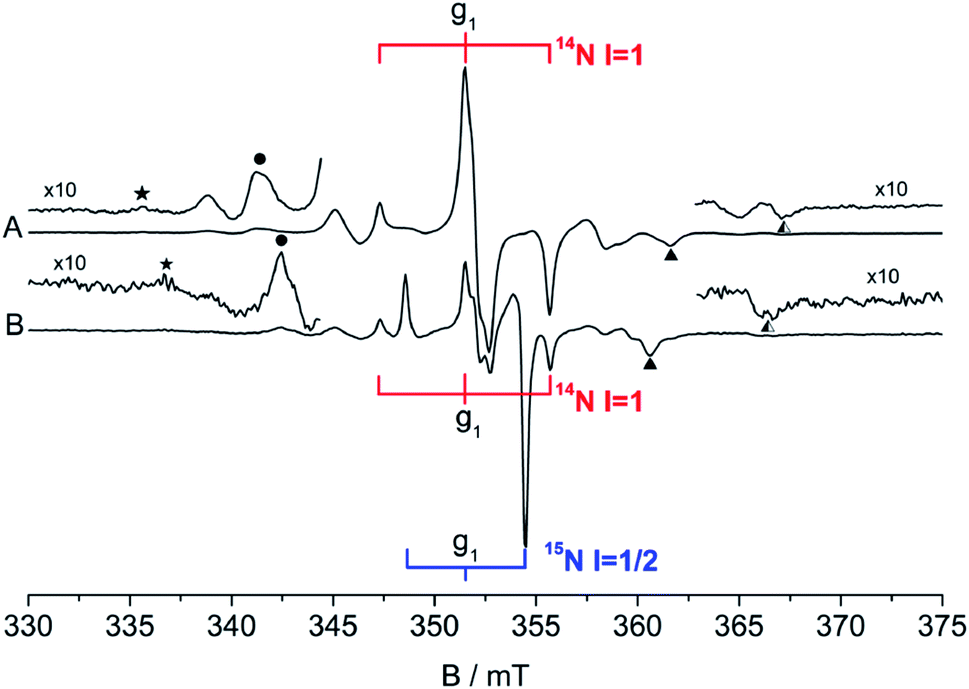 | ||
| Fig. 10 CW-EPR spectra of the N centre in SnO2. (A) 14N, (B) 70% 15N, 30% 14N. | ||
This additional hyperfine structure arises from the presence of two non-zero nuclear spin isotopes of Sn, namely 117Sn and 119Sn having 7.68% and 8.59% natural abundance respectively. Both isotopes have I = 1/2 and similar nuclear magnetic moment. For these reasons, the system can be therefore treated as containing 16.27% of a I = 1/2 “magnetic” Sn (hereafter *Sn). The presence of a Sn hyperfine structure allows the obtainment of some important geometrical constrains concerning the coordination of the N centre in the structure. The experimental spectra have been simulated considering the N ion surrounded by three Sn cations. This assumption is valid, in a rutile-like structure, both for a substitutional and an interstitial defect. Three distinct models of N coordination have been considered: (a) three equivalent Sn ions, (b) two equivalent Sn, (c) three inequivalent Sn. The correspondence between magnetic (hyperfine) equivalence and structural equivalence was also assumed. The existence of both Sn (I = 0) and *Sn (I = 1/2) nuclei imply the presence of distinct isotopomers (containing respectively zero, one, two and three magnetic Sn ions around each nitrogen) whose statistical abundance, to be introduced in the simulation procedure, is derived by combinatorial formulas. As an example, if the three Sn ions are structurally equivalent one has the following arrangement of isotopomers: (i) N SnSnSn ab. = 0.582; N *SnSnSn ab. = 0.345; N *Sn*SnSn ab. = 0.068; N *Sn*Sn*Sn ab. = 0.0045. By comparing the simulated spectra of all possible structural combinations with the experimental data, the best fit was obtained for three equivalent Sn ions around the N centre. It is to note that the possibility of a slight structural (=magnetic) difference between the three ions, although not large enough to be detected in a powder spectrum, cannot be discarded solely on the basis of this fitting procedure.
The full set of spin-Hamiltonian parameters is collected in Table 5, while Fig. 11 reports the simulation of the experimental spectra (14N and 15N) obtained using these parameters. In order to definitely provide a structural model for the observed defect, B3LYP-DFT calculations have been performed on three possible structures for the N–SnO2 centre: one substitutional N (Nsub) and the two others interstitial N (Nint). Note that the latter possibilities automatically imply the formation of N–O bonds.
| N–SnO2 | g 1 | g 2 | g 3 | Isotope | A 1/mT | A 2/mT | A 3/mT | ρ(N)b | ρ (Sn 5s) |
|---|---|---|---|---|---|---|---|---|---|
| a The reported calculated values are the average of three values (one for each Sn) with small differences (<6%) between sites. b The experimental spin density values are evaluated by comparison with the corresponding atomic hyperfine values while the computed ones directly derive from Mulliken analysis. | |||||||||
| Experimental | 2.0053 | 2.0023 | 1.9978 | 14N | 4.17 | 0.083 | 0.078 | 0.77 | |
| 15N | 5.88 | 0.117 | 0.110 | 0.77 | |||||
| 117Sn | 11.7 | 12.3 | 11.9 | 0.008 | |||||
| 119Sn | 12.2 | 12.8 | 12.4 | 0.008 | |||||
| Computed (substitutional N) | 14N | 4.59 | 0.439 | 0.420 | 0.99 | ||||
| 117Sna | 8.60 | 9.57 | 8.66 | 0.022 | |||||
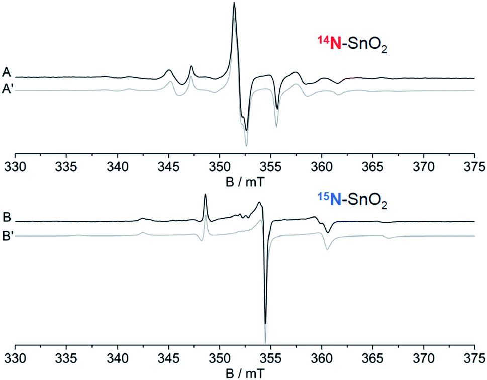 | ||
| Fig. 11 CW-EPR experimental spectra and corresponding computer simulations (rash-dotted traces) of the N centre in SnO2 obtained using 14N (A and A′) and 15N (B and B′) respectively. | ||
Surprisingly, the N A constants were not very different for the three structures and therefore did not favour any of the three models. On the other hand, only the Sn A constants calculated for the Nsub case show three nearly equivalent Sn centres around the N in agreement with the experiment. In conclusion, the analysis of the rich hyperfine structure of the EPR spectra in conjunction with the DFT calculations indicate that in SnO2 the nitrogen substitutes for oxygen and is surrounded by three nearly equivalent Sn atoms (Fig. 12). From an electronic point of view, the unpaired electron is strongly localized on the N nucleus (0.77, Table 5) and only partially extends on the surrounding Sn cations. It is to note that the resolved Sn superhyperfine structure is essentially due to Fermi contact and corresponds just to a small fraction of the whole spin density. It actually monitors a tail of the unpaired electron wavefunction which leaks from the 2p orbital of N to the 5s orbitals of the Sn ions. Although the spin density on each Sn ion is small, the corresponding A coupling manifest in the spectrum due to the extremely high atomic constants of both 117Sn and 119Sn nuclei.
 | ||
| Fig. 12 Schematic view of the substitutional N centre (blue ball) in SnO2 (Sn = yellow, oxygen = red) in dioxide and of the corresponding electron spin density. | ||
7. N doping of zirconium titanate and other oxides
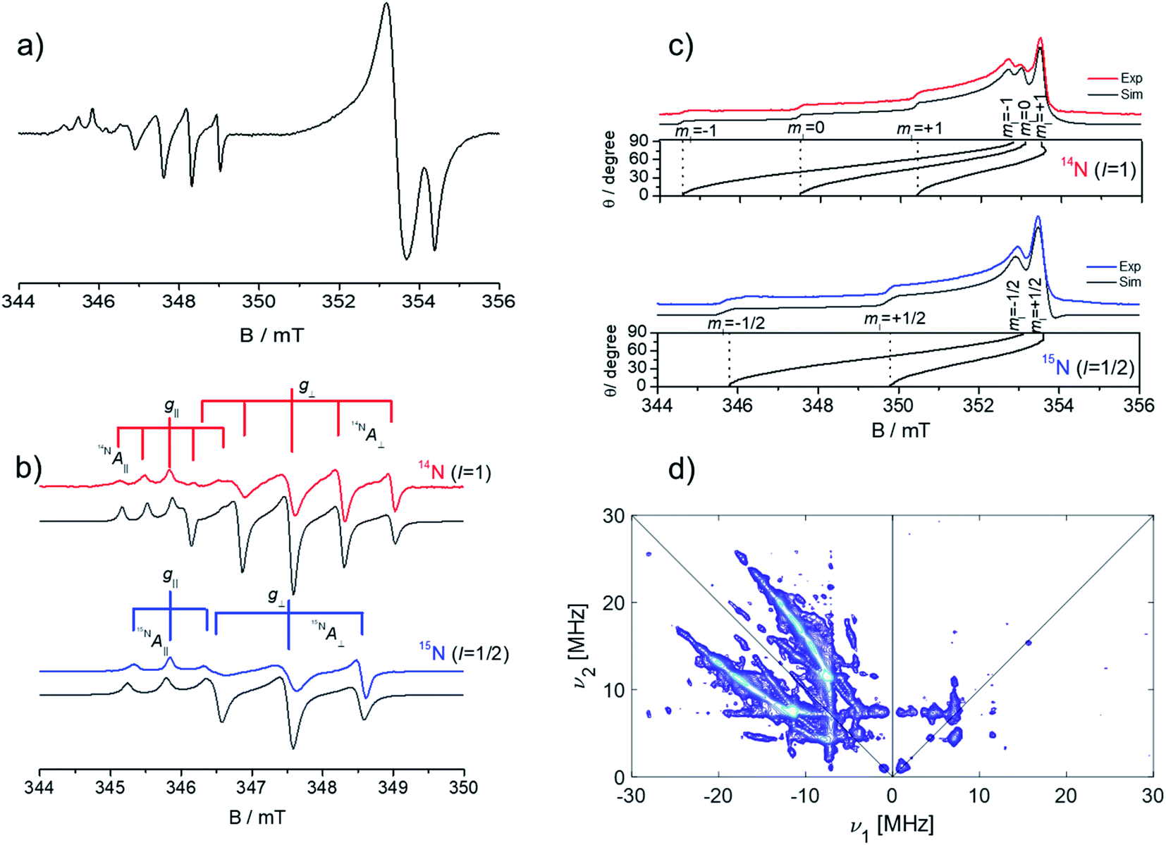
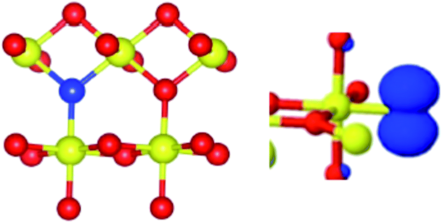
Zirconium titanate (ZrTiO4) is a stable ternary compound in the ZrO2–TiO2 phase diagram exhibiting the scrutinyite structure. The latter structure is analogous to those shown by the more known polymorphs of TiO2 and is also based on MeO6 octahedra (Me = Ti, Zr) linked by three-coordinated oxygen (OMe3).91 The tetravalent Ti and Zr cations are randomly distributed within the lattice. ZrTiO4 is used in technological application as a capacitor, an oscillator or a dielectric resonator and in optical devices.92 The incorporation of nitrogen in the lattice of ZrTiO4 has been performed in an effort to produce a system potentially photoactive under visible light with a more favourable reduction potential with respect to TiO2. The 3.6 eV band gap value of pristine ZrTiO4 and the reduction potential of the conduction band are both slightly higher than that of TiO2. The sol–gel protocol entailed the use of titanium isopropoxide as main component and controlled amounts of ZrOCl2 and NH4Cl. The solid obtained after the final calcination shows a pronounced optical absorption in the visible region with a maximum at 430 nm. This band, which is completely absent in pristine ZrTiO4, partially overlaps with the bandgap transition (Fig. 13). The solid is also EPR active and the observed spectrum is ascribable to a species containing a single N atom with spectral parameters analogous, though not coincident, to those observed for N–TiO2. Fig. 13 shows CW-EPR spectra recorded at two different frequencies, 9.5 GHz (X-band) and 35 GHz (Q-band), and using both 14N and 15N.93 The simulation of the four distinct spectra was performed using the same set of spin-Hamiltonian parameters producing an accurate set of g and A values that is reported in Table 6. The g values are extremely close one another and fall in the range 2.0081–2.0038, whereas the A tensor is rhombic with one component much larger than the remaining two.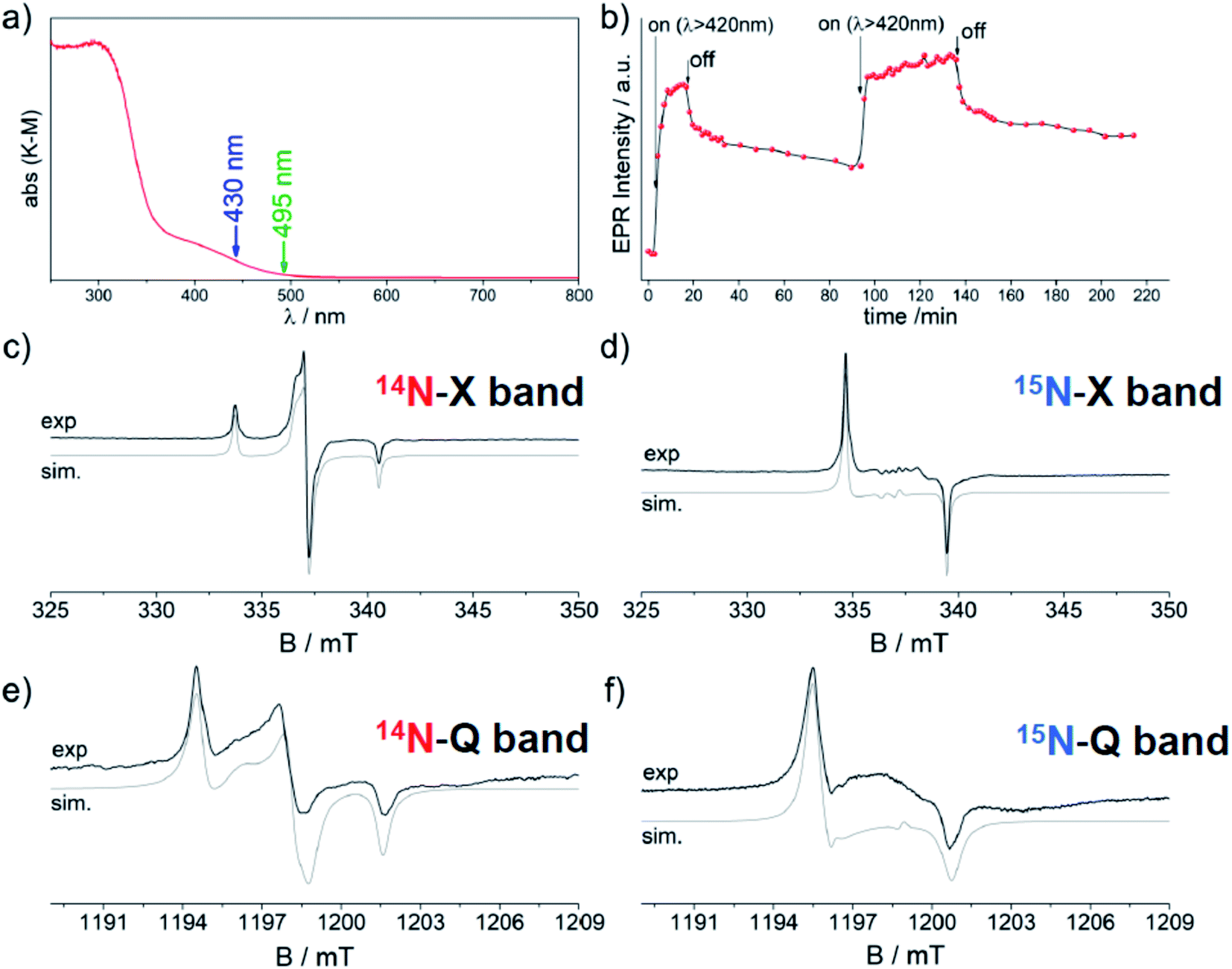 | ||
| Fig. 13 UV-Vis absorption of N–ZrTiO4 (a) and EPR experimental and computer simulated spectra (c–f). EPR spectra are related to the defects containing 14N (c and e) or 15N (d and f) and in both cases are recorded at 9.5 GHz (X-band) or 35 GHz (Q band). Top (b): changes of the EPR signal intensity of the N defect in ZrTiO4 under irradiation with polychromatic visible light (λ > 420 nm). | ||
| N–ZrTiO4 | g 1 | g 2 | g 3 | Isotope | A 1/mT | A 2/mT | A 3/mT | ρ(N 2p) | ρ(N 2s) |
|---|---|---|---|---|---|---|---|---|---|
| Experimental | 2.0081 | 2.0046 | 2.0038 | 14N | 0.22 | 3.40 | 0.16 | 0.67 | 0.02 |
| 15N | 0.32 | 4.90 | 0.26 | 0.67 | 0.02 | ||||
| Computed. Interstitial N (schemes in Fig. 10) | 14N (1) | −0.358 | 3.369 | −0.195 | |||||
| 14N (2) | −0.510 | 3.459 | −0.377 | ||||||
The A values indicate a total spin density on the N atom amounting to 0.69 with the major contribution on the N 2p orbital (0.67) and a minor one (0.02) on the 2s orbital. Also in this case the comparison of DFT prediction with the experimental values was used to definitely assign the N defect to a substitutional or an interstitial position. The best agreement was found for the interstitial case, since the calculated hyperfine parameters correctly reproduced the experimental results. Given the statistical distribution of Ti4+ and Zr4+ cations in ZrTiO4, DFT calculations were performed for two sites, which differed for the cationic coordination sphere around the interstitial N as shown in Fig. 14. Interestingly both cases yielded very similar EPR parameters both in good agreement with the experiment.
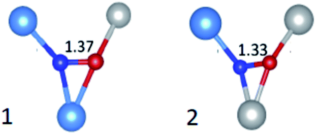 | ||
| Fig. 14 Schemes of the two statistically more abundant interstitial N defects in ZrTiO4 with N–O bond length in Å. Ti are in gray, Zr in light blue, N in blue and O in red. | ||
Similar to TiO2, the N centre is described as a charged species displaying NO molecular orbitals with the electron spin density (ρ) localized on one of the two π* orbitals of the NO fragment, which lies ca. 1 eV above the valence band.
The N defect individuated by EPR is photosensitive to visible light as indicated by its growth upon irradiation with light of wavelength higher than 420 nm (Fig. 13b). The increase of EPR intensity upon irradiation is explained, in line with N–TiO2 (Section 4.3), by assuming that diamagnetic 2-electron centres are also present and more abundant than paramagnetic ones. The former are preferentially depopulated by monochromatic irradiation as reported in eqn (3), Fig. 5 and 13b.
8. N doping and influence on the physical properties of semiconducting oxides
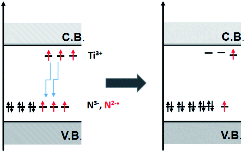
All the nitrogen defects in semiconducting oxides reviewed in the previous sections display some common features that can be resumed as follows: (a) the N impurity form intra band gap levels close to the VB limit; (b) the paramagnetic shallow acceptor levels (N2−˙, NO2−˙) is often accompanied by their reduced (two-electron) and diamagnetic counterparts (N3−, NO3−); (c) electrons from these states are promoted to the CB by specific irradiation in the visible; (d) moreover all the oxides here considered contain, though at different extent, shallow donor levels due to impurities and/or lack of stoichiometry.A key take home message is that, in semiconducting oxides, shallow donors are not independent from acceptor levels. A clear example is provided by F–N–TiO2 (Section 4.3). Fluorine bears one extra electron with respect to oxygen and generates shallow donors levels close to the CB that can be detected via EPR as Ti3+ centres.56 When TiO2 is co-doped with N and F a synergic effect between the two dopants is observed since the presence of one dopant favours the insertion of the other. This is due to the stabilisation of the extra electrons on Ti3+ that move from the shallow donor levels to the low-lying levels of the N acceptors. DFT calculations corroborate this interpretation and point to a net reduction of the energy cost of doping in the presence of both dopants,55 identifying the driving force of the process in the lower total electron energy resulting from the described synergy, as illustrated in Fig. 15.
 | ||
| Fig. 15 Schematic view of the electron shallow donor scavenging from shallow donor states to low lying impurity states. | ||
For similar reasons, doped oxides are more prone to the formation of oxygen vacancies as compared to the pristine solid. It is well known in fact that semiconducting oxides are in equilibrium with molecular oxygen. A stoichiometric semiconducting oxide always releases oxygen in the gas phase with the concomitant formation of oxygen vacancies and excess electrons in the solid, with an equilibrium constant that depends on the given experimental conditions.
For an oxide with MeO2 stoichiometry, the process of oxygen release can be summarized by the equation:
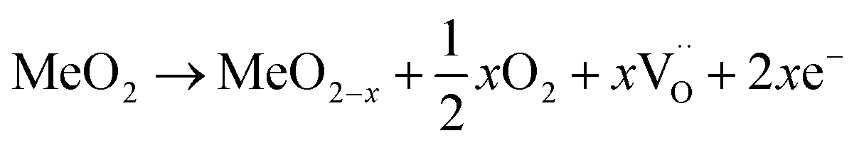 | (8) |
 represents a doubly positive oxygen vacancy, and all other symbols have their usual chemical meaning. In pristine TiO2, the calculated energy cost for the creation of an oxygen vacancy according to eqn (8) is 4.2 eV. This energy drops dramatically to 0.6 eV in the case of N–TiO2.38. The process becomes so much less energy demanding because the low-lying levels, due to N doping, scavenge the excess electrons produced by oxygen release. This also explains the coexistence of variable ratios of one-electron and two-electron N levels, within the lattice of N doped oxides (Sections 4.2 and 5).
Crucially, these considerations frustrate the idea of using nitrogen doping to synthetize stable p-type semiconducting oxides and system with efficient collective magnetic behaviours. The former application requires hole states close to the valence band, the latter an array of paramagnetic centres in mutual connection. In both cases one-electron (paramagnetic) states are essential, two-electron (diamagnetic) states detrimental.
The hurdle is particularly dramatic for SnO2. Surprisingly the n-type character of N– SnO2 is in fact higher than that of pristine SnO2. This has been shown in a systematic study on N–SnO2 employing optical, EPR, XPS and UPS spectroscopies.94 As shown in Fig. 16, the UPS spectrum of N–SnO2, after an oxidative treatment performed to attain an oxidation as close as possible to the stoichiometry (Fig. 16e), appears very similar to that of undoped SnO2 subject to prolonged reductive vacuum annealing treatments at high temperature (Fig. 16d).
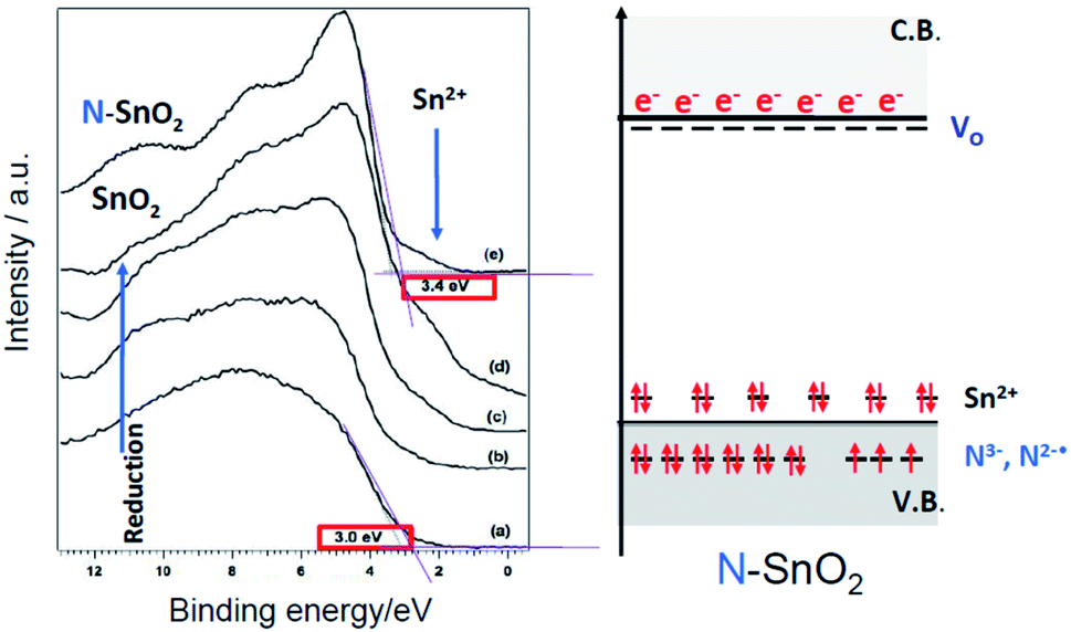 | ||
| Fig. 16 Left: Comparison between the UPS spectra of as prepared SnO2 (a) treated at increasing temperature under vacuum from 623 K to 823 K (b–d) and the spectrum of as prepared N–SnO2 (e). The shoulder at 3.4 eV due to Sn2+ is indicated by an arrow. Right: Scheme of the energy levels in N–SnO2. Figure adapted from ref. 57. | ||
The peculiar behaviour of N–SnO2 is due to the chemistry of Sn and its ability to form stable Sn(II) states lying close to the valence band maximum. The simultaneous presence of the two types of potential electron acceptors (N2−˙ and Sn4+) dramatically decreases the energy cost for the formation of oxygen vacancies and increases the amount of excess electrons in the system. A fraction of those electrons is stabilized at low energy under the form of N3− and Sn2+ (Fig. 16) while the remaining stays at high energy, easily ionized in the conduction band as indicated by absorption in the NIR.94 This description accounts for the apparently paradoxical behaviour of N–SnO2 and the evident difficulties to prepare p-type system or systems displaying collective magnetic properties simply by nitrogen doping. To the best of our knowledge, for the former case there is a single literature report claiming the achievement of a p-type N–SnO2 while, for the latter, all paper reporting ferromagnetic (or antiferromagnetic) behaviour of N impurities are solely based on theoretical calculations considering an ideal matrix. On the other hand, ZnO seems a more promising candidate. For this system some success in obtaining p-type conduction64–66 or ferromagnetic states69 by N doping is asserted in the literature. However, as reported by T. M. Barnes et al.,65 the conduction property tends to decline over time, indicating a possible progressive rearrangement of the electronic structure. Therefore, the synthesis of highly pure ZnO crystals, with negligible presence of shallow donors impurities, is probably key to succeed in obtaining p-type materials by N doping.
In summary, the interplay between paramagnetic one-electron states (N2−˙ or NO2−˙) and diamagnetic ones (N3− or NO3−) is the key feature to understand the properties of N doped semiconducting oxides. This interplay extends also to the photochemical properties of N doped semiconducting oxides. As seen in Sections 4.2, 5.1 and 7, the intensity of the EPR signal of the paramagnetic centres in TiO2,45 ZnO76 and ZrTiO4 (ref. 93) increases under irradiation due to the excitation of electrons from N3− states to the conduction band, with a concomitant formation of additional N2− acceptor states. This observation nicely agrees with the remarkable experimental observation by Yu et al.95 which reports an increase of ferromagnetism in UV-irradiated N–ZnO films accompanied by a decrease of resistivity (i.e. onset of p-type conduction). The process appears fully reversible as the initial situation is progressively recovered once the irradiation is interrupted. This experiment fully confirms the picture that was originally derived solely through EPR data, as explained in this and previous sections.
9. Conclusions
This Perspective presented some relevant examples of nitrogen insertion into the bulk of semiconducting oxides. Firstly, we have provided a concise summary of the preparation procedures used to insert nitrogen defects in various matrices. Secondly, we have shown that EMR techniques are extremely appropriate for the fine description of defective sites in solid lattices. These sites are particularly elusive chemical entities randomly distributed and present at low (or very low) concentrations. We have also documented that a full description of the geometrical and electronic structure of such defects can be obtained by an integrated use of EMR techniques and DFT computations. This allows the identification of a unique structural model when multiple sites can in principle be formed. In turn, this synergic approach provides a true structural insight especially useful when other more commonly used techniques fail. Beside the structural characterization of the N defects (Sections 4–7), we have also discussed (Section 8) the influence of the doping with N (an electron acceptor) on the general properties of the oxides. In particular, we have addressed how low-lying N energy states withdraw electrons from shallow donor states and decrease the energy cost for the formation of oxygen vacancies, hampering the synthesis p-type oxide semiconductors.Assembling a systematic and general analysis concerning the insertion of N into metal oxides is not straightforward. We note that other metal oxides have been doped with nitrogen for applications in various areas (ceramics, microelectronics, catalysis and photocatalysis), these include: indium oxide (InO2),96 cuprous oxide (Cu2O),97 tungsten trioxide (WO3)98 and cerium dioxide (CeO2).99 However, no direct characterization of N defects, in particular with EMR methods, is available in the literature for these systems. In any way, on the basis of the examples reported it may be tempting to infer that oxide more prone to incorporate monoatomic nitrogen defects contain low coordinated oxygen ions in their structure. All the examples of N doping described here concern oxides having 3- or 4-coordinated oxygen ions such as TiO2 (anatase and rutile, O3c, Section 4), ZnO (wurtzite, O4c, Section 5), SnO2 (rutile, O3c, Section 6), ZrTiO4 (scrutinyite, O3c, Section 7). Low coordination oxygen ions are also found in the above mentioned cases of WO3 (O2c), Cu2O (O4c), In2O3 (O4c). These evidences clearly suggest that nitrogen insertion is easier in the case of relatively open structures than in those showing high coordination numbers, in particular when preparation procedures based on wet-chemistry methods are employed.
Conflicts of interest
There are no conflicts to declare.Acknowledgements
We gratefully acknowledge longstanding collaborations and many useful discussions with Gianfranco Pacchioni and Cristiana Di Valentin (University of Milano Bicocca), Elena Selli (University of Milano), Gaetano Granozzi and Stefano Agnoli (University of Padova).References
- E. Burke, A Philosophical Inquiry into the Origin of our Ideas of the Sublime and Beautiful, Oxford University Press, 1990, Part III, Section IX: “Perfection not the cause of Beauty”, p. 100 Search PubMed.
- T. H. Maiman, Nature, 1960, 187, 493 CrossRef.
- Power Electronics Device Applications of Diamond Semiconductors, ed. S. Koizumi, H. Umezawa, J. Pernot and M. Suzuki, Woodhead Publishing, 2018, DOI:10.1016/c2016-0-03999-2.
- Y. N. Palyanov, Y. M. Borzdov, A. F. Khokhryakov, I. N. Kupriyanov and A. G. Sokol, Cryst. Growth Des., 2010, 10, 3169 CrossRef CAS.
- G. Feher, Phys. Rev., 1959, 114, 1219 CrossRef CAS.
- J. M. Baker and M. Newton, Appl. Magn. Reson., 1995, 8, 207 CrossRef CAS.
- J. D. Breeze, E. Salvadori, J. Sathian, N. M. Alford and C. W. M. Kay, Nature, 2018, 555, 493 CrossRef CAS PubMed.
- M. Chiesa and E. Giamello, in Electron Paramagnetic Resonance, A practitioner's toolkit, ed. M. Brustolon and E. Giamello, John Wiley and Sons, 2009 Search PubMed.
- M. Chiesa, E. Giamello, S. Livraghi, M. C. Paganini and E. Salvadori, J. Phys.: Condens. Matter, 2019, 31, 444001 CrossRef CAS PubMed.
- J.-M. Spaeth and H. Overhof, Point Defects in Semiconductors and Insulators, Springer, 2003 Search PubMed.
- S. Sakthivel, M. Janczarek and H. J. Kisch, J. Phys. Chem. B, 2004, 108, 19384 CrossRef CAS.
- T. Okumura, Y. Kinoshita, H. Uchiyama and H. Imai, Mater. Chem. Phys., 2008, 111, 486 CrossRef CAS.
- S. Yin, Y. Aita, M. Komatsu and T. Sato, J. Eur. Ceram. Soc., 2006, 26, 2735 CrossRef CAS.
- Y. Hirose, A. Itadani, T. Ohkubo, H. Hashimoto, J. Takada, S. Kittaka and Y. Kurod, Dalton Trans., 2017, 46, 4435 RSC.
- S. Indris, R. Amade, P. Heitjans, M. Finger, A. Haeger, D. Hesse, W. Grunert, A. Borger and K. D. Becker, J. Phys. Chem. B, 2005, 109, 23274 CrossRef CAS PubMed.
- G. Liu, F. Li, Z. Chen, G. Q. Lu and H. M. Cheng, J. Solid State Chem., 2006, 179, 331 CrossRef CAS.
- Y. Sakatani, J. Nunoshige, H. Ando, K. Okusako, H. Koike, T. Takata, J. N. Kondo, M. Hara and K. Domen, Chem. Lett., 2003, 32, 1156 CrossRef CAS.
- Y. Wang, C. Feng, Z. Jin, J. Zhang, J. Yang and S. Zhang, J. Mol. Catal. A: Chem., 2006, 160, 1 CrossRef.
- H. M. Yates, M. G. Nolan, D. W. Sheel and M. E. Pemble, J. Photochem. Photobiol., A, 2006, 179, 213 CrossRef CAS.
- O. Diwald, T. L. Thompson, E. G. Goralski, S. D. Walck and J. T. Yates, J. Phys. Chem. B, 2004, 108, 52 CrossRef CAS.
- M. Batzill, E. H. Morales and U. Diebold, Phys. Rev. Lett., 2006, 96, 026103 CrossRef PubMed.
- J. M. Mwabora, T. Lindgren, E. Avendano, T. F. Jaramillo, J. Lu, S. E. Lindquist and C. G. Granqvist, J. Phys. Chem. B, 2004, 108, 20193 CrossRef CAS.
- Y. Nakano, T. Morikawa, T. Ohwaki and Y. Taga, Appl. Phys. Lett., 2005, 86(1–3), 132104 CrossRef.
- R. Asahi and T. Morikawa, Chem. Phys., 2007, 339, 57 CrossRef CAS.
- S. Livraghi, M. Pelaez, J. Biedrzycki, I. Corazzari, E. Giamello and D. D. Dionysiou, Catal. Today, 2013, 209, 54 CrossRef CAS.
- Q. Wang and K. Domen, Chem. Rev., 2020, 120, 919 CrossRef CAS PubMed.
- J. Schneider, M. Matsuoka, M. Takeuchi, J. Zhang, Y. Horiuchi, M. Anpo and D. W. Bahnemann, Chem. Rev., 2014, 114, 9919 CrossRef CAS PubMed.
- M. Gratzel, Acc. Chem. Res., 2009, 42, 1788 CrossRef CAS PubMed.
- M. Cho, H. Chung, W. Choi and J. Yoon, Water Res., 2004, 38, 1069 CrossRef CAS PubMed.
- U. Diebold, Surf. Sci. Rep., 2003, 48, 53 CrossRef CAS.
- G. Liu, H. G. Yang, J. Pan, Y. Q. Yang, G. Q. Lu and H.-M. Cheng, Chem. Rev., 2014, 114, 9559 CrossRef CAS PubMed.
- S. Sato, Chem. Phys. Lett., 1986, 123, 126 CrossRef CAS.
- R. Asahi, T. Morikawa, T. Ohwaki, K. Aoki and Y. Taga, Science, 2001, 293, 269 CrossRef CAS PubMed.
- N. C. Saha and H. G. Tompkins, J. Appl. Phys., 1992, 72, 3072 CrossRef CAS.
- W. Wang, M. O. Tadé and Z. Shao, Prog. Mater. Sci., 2018, 92, 33 CrossRef CAS.
- R. Asahi, T. Morikawa, H. Irie and T. Ohwaki, Chem. Rev., 2014, 114, 9824 CrossRef CAS PubMed.
- S. Livraghi, A. Votta, M. C. Paganini and E. Giamello, Chem. Commun., 2005, 498 RSC.
- C. Di Valentin, G. Pacchioni, A. Selloni, S. Livraghi and E. Giamello, J. Phys. Chem. B, 2005, 109, 11414 CrossRef CAS PubMed.
- S. Livraghi, A. M. Czoska, M. C. Paganini and E. Giamello, J. Solid State Chem., 2009, 182, 160 CrossRef CAS.
- C. Pan, T. Takata, M. Nakabayashi, T. Matsumoto, N. Shibata, Y. Ikuhara and K. Domen, Angew. Chem., Int. Ed., 2015, 54, 2955 CrossRef CAS PubMed.
- Y. Liu, W. Wang, X. Xu, J. Marcel Veder and Z. Shao, J. Mater. Chem. A, 2019, 7, 7280 RSC.
- F. Napoli, M. Chiesa, S. Livraghi, E. Giamello, S. Agnoli, G. Granozzi, G. Pacchioni and C. Di Valentin, Chem. Phys. Lett., 2009, 477, 435 CrossRef.
- S. Livraghi, M. R. Chierotti, E. Giamello, G. Magnacca, M. C. Paganini, G. Cappelletti and C. L. Bianchi, J. Phys. Chem. C, 2008, 112, 17224 CrossRef.
- T. Sekiya, N. Kamiya, S. Ohya, S. Kurita and T. Kodayra, J. Phys. Soc. Jpn., 2009, 78, 114701 CrossRef.
- S. Livraghi, M. C. Paganini, M. Chiesa, E. Giamello, A. Selloni, C. Di Valentin and G. Pacchioni, J. Am. Chem. Soc., 2006, 128, 15666 CrossRef CAS PubMed.
- G. Barolo, S. Livraghi, M. Chiesa, M. C. Paganini and E. Giamello, J. Phys. Chem. C, 2012, 116, 20887 CrossRef CAS.
- S.-K. Joung, T. Amemiya, M. Murabayashi and K. Itoh, Appl. Catal., A, 2006, 312, 20 CrossRef CAS.
- E. A. Reyes-Garcia, Y. Sun, K. Reyes-Gil and D. Raftery, J. Phys. Chem. C, 2007, 111, 2738 CrossRef CAS.
- E. A. Konstantinova, A. I. Kokorin, K. Lips, S. Sakthivel and H. Kisch, Appl. Magn. Reson., 2009, 35, 421 CrossRef CAS.
- M. Pelaez, P. Falaras, V. Likodimos, A. G. Kontos, A. A. de la Cruz, K. O'Shead and D. D. Dionysious, Appl. Catal., B, 2010, 99, 378 CrossRef CAS.
- G. Yang, Z. Jiang, H. Shi, T. Xiao and Z. Yan, J. Mater. Chem., 2010, 20, 5301 RSC.
- Z. Barbieriková, E. Pližingrová, M. Motlochová, P. Bezdička, J. Boháček, D. Dvoranová, M. Mazúr, J. Kupčík, J. Jirkovský, J. Šubrt, J. Krýsa and V. Brezová, Appl. Catal., B, 2018, 232, 397 CrossRef.
- M. D'Arienzo, N. Siedl, A. Sterning, R. Scotti, F. Morazzoni, J. Bernardi and O. Diwald, J. Phys. Chem. C, 2010, 114, 18067 CrossRef.
- D. Li, H. Haneda, S. Hishita and N. Ohashi, Chem. Mater., 2005, 17, 2588 CrossRef CAS.
- C. Di Valentin, E. Finazzi, G. Pacchioni, A. Selloni, S. Livraghi, A. M. Czoska, M. C. Paganini and E. Giamello, Chem. Mater., 2008, 20, 3706 CrossRef CAS.
- A. M. Czoska, S. Livraghi, M. C. Paganini, E. Giamello, S. Agnoli, G. Granozzi, E. Finazzi, C. Di Valentin and G. Pacchioni, J. Phys. Chem. C, 2008, 112, 8951 CrossRef CAS.
- A. Folli, J. Z. Bloh, E.-P. Beukes, R. F. Howe and D. E. Macphee, J. Phys. Chem. C, 2013, 117, 22149 CrossRef CAS.
- N. O. Gopal, H. H. Lo and S. C. Ke, J. Am. Chem. Soc., 2008, 130, 2760 CrossRef CAS PubMed.
- A. M. Czoska, S. Livraghi, M. Chiesa, E. Giamello, G. Pacchioni and C. Di Valentin, Phys. Chem. Chem. Phys., 2011, 13, 136 RSC.
- C. G. Van de Walle, Phys. Rev. Lett., 2000, 85, 1012 CrossRef CAS PubMed.
- A. Janotti and C. G. Van de Walle, Rep. Prog. Phys., 2009, 72, 126501 CrossRef.
- Y. Yan, S. B. Zhang and S. T. Pantelides, Phys. Rev. Lett., 2001, 86, 5723 CrossRef CAS PubMed.
- J. P. Zhang, L. D. Zhang, L. Q. Zhu, Y. Zhang, M. Liu, X. J. Wang and G. He, J. Appl. Phys., 2007, 102, 114903 CrossRef.
- Z. W. Wang, Y. Yue and Y. Cao, Vacuum, 2014, 101, 313 CrossRef CAS.
- T. M. Barnes, K. Olson and C. A. Wolden, Appl. Phys. Lett., 2005, 86, 112112 CrossRef.
- H. Zhang, C. Kong, W. Li, G. Qin, H. Ruan and M. Tan, J. Mater. Sci.: Mater. Electron., 2016, 27, 5251 CrossRef CAS.
- F. B. Zheng, C. W. Zhang, P. J. Wang and H. X. Luan, Solid State Commun., 2012, 152, 1199 CrossRef CAS.
- L. Shi, J. W. Jin and C. Y. Xu, Mod. Phys. Lett. B, 2010, 24, 2171 CrossRef CAS.
- K. Jindal, M. Tomar, R. S. Katiyar and V. Gupta, AIP Adv., 2015, 5, 027117 CrossRef.
- M. Wang, F. Ren, J. Zhou, G. Cai, L. Cai, Y. Hu, D. Wang, Y. Liu, L. Guo and S. Shen, Sci. Rep., 2015, 5, 12925 CrossRef CAS PubMed.
- A. Kobayashi, O. F. Sankey and J. D. Dow, Phys. Rev. B: Condens. Matter Mater. Phys., 1983, 28, 946 CrossRef CAS.
- A. Valour, F. Cheviré, F. Tessier, F. Grasset, B. Dierre, T. Jiang, E. Faulques, L. Caio and S. Jobic, Solid State Sci., 2016, 54, 30 CrossRef CAS.
- R. Kobayashi, T. Kishi, Y. Katayanagi, T. Yano and N. Matsushita, RSC Adv., 2018, 8, 23599 RSC.
- D. Pfisterer, J. Sann, D. M. Hofmann, M. Plana, A. Neumann, M. Lerch and B. K. Meyer, Phys. Status Solidi B, 2006, 243, R1–R3 CrossRef CAS.
- W. E. Carlos, E. R. Glaser and D. C. Look, Phys. B, 2001, 308, 976 CrossRef.
- N. Y. Garces, N. C. Giles, L. E. Halliburton, G. Cantwell, D. B. Eason, D. C. Reynolds and D. C. Look, Appl. Phys. Lett., 2002, 80, 1334 CrossRef CAS.
- N. Y. Garces, L. Wang, N. C. Giles, L. E. Halliburton, G. Cantwell and D. B. Eason, J. Appl. Phys., 2003, 94, 519 CrossRef CAS.
- X. H. Li, H. Y. Xu, X. T. Zhang, Y. C. Liu, J. W. Sun and Y. M. Lu, Appl. Phys. Lett., 2009, 95, 191903 CrossRef.
- F. Gallino, C. Di Valentin, G. Pacchioni, M. Chiesa and E. Giamello, J. Mater. Chem., 2010, 20, 689 RSC.
- F. Napoli, M. Chiesa, E. Giamello, M. Fittipaldi, C. Di Valentin, F. Gallino and G. Pacchioni, J. Phys. Chem. C, 2010, 114, 5187 CrossRef CAS.
- E. Comini, G. Faglia and G. Sberveglieri, Sens. Actuators, 2001, 78, 73 CrossRef CAS.
- S. Gubbala, V. Chakrapani, V. Kumar and M. K. Sunkara, Adv. Funct. Mater., 2008, 18, 2411 CrossRef CAS.
- Y. Idota, T. Kubota, A. Matsufuji, Y. Maekawa and T. Miyasaka, Science, 1997, 276, 1395 CrossRef CAS.
- S. S. Pan, C. Ye, X. M. Teng, L. Li and G. H. Li, Appl. Phys. Lett., 2006, 89, 251911 CrossRef.
- X. Sun, R. Long, X. Cheng, X. Zhao, Y. Dai and B. Huang, J. Phys. Chem. C, 2008, 112, 9861 CrossRef CAS.
- S. S. Pan, G. H. Li, L. B. Wang, Y. D. Shen, Y. Wang, T. Mei and X. Hu, Appl. Phys. Lett., 2009, 95, 222112 CrossRef.
- B. Zhou, S. Dong, H. Zhao, Y. Liu and P. Wu, Magn. Mater., 2014, 362, 14 CrossRef CAS.
- R. Long and N. J. English, Phys. Lett. A, 2009, 374, 319 CrossRef CAS.
- S. Zhang, J. Li, H. Niu, W. Xu, J. Xu, W. Hu and X. Wang, ChemPlusChem, 2013, 78, 192 CrossRef CAS.
- E. Albanese, C. Di Valentin, G. Pacchioni, F. Sauvage, S. Livraghi and E. Giamello, J. Phys. Chem. C, 2015, 119, 26895 CrossRef CAS.
- J. L. Lyons, A. Janotti and C. G. Van der Walle, Appl. Phys. Lett., 2009, 95, 252105 CrossRef.
- L. X. Guan, J. G. Tao, C. H. A. Huan, J. L. Kuo and L. Wang, Appl. Phys. Lett., 2009, 95, 012509 CrossRef.
- V. Poliotto, E. Albanese, S. Livraghi, G. Pacchioni and E. Giamello, J. Mater. Chem. A, 2017, 5, 13062 RSC.
- S. Livraghi, N. Barbero, S. Agnoli, C. Barolo, G. Granozzi, F. Sauvage and E. Giamello, Phys. Chem. Chem. Phys., 2016, 18, 22617 RSC.
- C. F. Yu, S. J. Sun, H. S. Hsu and H. Chou, Phys. Lett. A, 2016, 380, 1872 CrossRef.
- S. Cho, J. Nanosci. Nanotechnol., 2017, 17, 4048 CrossRef CAS.
- Y. S. Lee, J. Heo, M. T. Winkler, S. C. Siah, S. B. Kim, R. G. Gordon and T. Buonassisi, J. Mater. Chem. A, 2013, 48, 15416 RSC.
- M. Takeuchi, Y. Shimizu, H. Yamagawa, T. Nakamuro and M. Anpo, Appl. Catal., B, 2011, 110, 1 CrossRef CAS.
- Y. Xu and R. Li, Appl. Surf. Sci., 2018, 455, 997 CrossRef CAS.
| This journal is © The Royal Society of Chemistry 2020 |