
 Open Access Article
 This Open Access Article is licensed under a Creative Commons Attribution-Non Commercial 3.0 Unported Licence
Ir6In32S21, a polar, metal-rich semiconducting subchalcogenide†
Jason F.
Khoury
 a,
Jiangang
He
b,
Jonathan E.
Pfluger
b,
Ido
Hadar
a,
Mahalingam
Balasubramanian
c,
Constantinos C.
Stoumpos
d,
Rui
Zu
e,
Venkatraman
Gopalan
ef,
Chris
Wolverton
b and
Mercouri G.
Kanatzidis
*a
a,
Jiangang
He
b,
Jonathan E.
Pfluger
b,
Ido
Hadar
a,
Mahalingam
Balasubramanian
c,
Constantinos C.
Stoumpos
d,
Rui
Zu
e,
Venkatraman
Gopalan
ef,
Chris
Wolverton
b and
Mercouri G.
Kanatzidis
*a
aDepartment of Chemistry, Northwestern University, Evanston, Illinois 60208, USA. E-mail: m-kanatzidis@northwestern.edu
bDepartment of Materials Science and Engineering, Northwestern University, Evanston, Illinois 60208, USA
cAdvanced Photon Source, Argonne National Laboratory, Argonne, Illinois 60439, USA
dDepartment of Materials Science and Technology, Voutes Campus, University of Crete, Heraklion, GR-70013, Greece
eDepartment of Materials Science and Engineering, Materials Research Institute, Pennsylvania State University, University Park, Pennsylvania 16802, USA
fDepartment of Physics, Pennsylvania State University, University Park, Pennsylvania 16802, USA
First published on 10th December 2019
Abstract
Subchalcogenides are uncommon, and their chemical bonding results from an interplay between metal–metal and metal–chalcogenide interactions. Herein, we present Ir6In32S21, a novel semiconducting subchalcogenide compound that crystallizes in a new structure type in the polar P31m space group, with unit cell parameters a = 13.9378(12) Å, c = 8.2316(8) Å, α = β = 90°, γ = 120°. The compound has a large band gap of 1.48(2) eV, and photoemission and Kelvin probe measurements corroborate this semiconducting behavior with a valence band maximum (VBM) of −4.95(5) eV, conduction band minimum of −3.47(5) eV, and a photoresponse shift of the Fermi level by ∼0.2 eV in the presence of white light. X-ray absorption spectroscopy shows absorption edges for In and Ir do not indicate clear oxidation states, suggesting that the numerous coordination environments of Ir6In32S21 make such assignments ambiguous. Electronic structure calculations confirm the semiconducting character with a nearly direct band gap, and electron localization function (ELF) analysis suggests that the origin of the gap is the result of electron transfer from the In atoms to the S 3p and Ir 5d orbitals. DFT calculations indicate that the average hole effective masses near the VBM (1.19me) are substantially smaller than the average electron masses near the CBM (2.51me), an unusual feature for most semiconductors. The crystal and electronic structure of Ir6In32S21, along with spectroscopic data, suggest that it is neither a true intermetallic nor a classical semiconductor, but somewhere in between those two extremes.
Introduction
Chalcogenides and intermetallics are two prominent and distinct classes of materials with very different bonding behaviors. Chalcogenides are generally valence precise semiconductors with covalent and ionic bonding interactions, while intermetallics tend to display metallic behavior because of extensive metal–metal bonding, leading to poorly defined formal oxidation states and partially occupied bands at the Fermi level.1–5 Subvalent (or metal-rich) materials are in the middle of the spectrum between these two extremes, as they have both metal–metal and metal-main group (e.g. chalcogenide, halide, oxide) bonding, with the oxidation states of the metal atoms being lower than what one might expect from the N-8 rule.6,7 The non-integer or low oxidation states, combined with structural confinement from the anionic species, can lead to special physical phenomena, such as confined metals, topological insulators, and charge density wave behavior.8–11 For example, the recently discovered subchalcogenide Ir2In8S is a Dirac semimetal candidate, spurring interest in finding more subvalent quantum materials.12 A large amount of electronegative main group atoms in a structure can tip the balance from metallic to insulating behavior, as is the case with subvalent compounds like PtIn7F13, Ir2In12Ga4O15, and Ru3Sn15O14.13–15 Finding new semiconducting subvalent materials is helpful in understanding how to control that balance and defining the origin of band gap formation in these materials.Subvalent compounds with main group elements have rich structural diversity, and harbor novel polar crystal structures given their diverse bonding motifs.7 Non-centrosymmetric (and in particular, polar) compounds are of great interest in the materials chemistry community because of properties such as ferroelectricity, piezoelectricity, and second harmonic generation (SHG).16 When a crystal lacks a center of symmetry and its atoms have strong spin–orbit coupling (SOC), the electronic structure can experience spin splitting in its bands, going from 2-fold degenerate to singly degenerate bands, often seen in Weyl semimetals (WSMs).17 This spin splitting is a quantum property and can be described as the Dresselhaus effect, the Rashba effect, or a combination of the two.18–21 Non-centrosymmetric but nonpolar crystal structures will only exhibit Dresselhaus spin-splitting, but a polar material can display both the Dresselhaus and Rashba effects in their electronic structures.20 Both the Rashba and Dresselhaus effect allow for control of the spin-splitting of a material via an external electric field, enabling the manipulation of both spin and charge degrees of freedom, a crucial requirement in assembling functional spintronic devices.22–26 The diverse quantum properties that can result from polar, non-centrosymmetric materials, especially with intermetallic bonding and high SOC, makes discovering new ones of great interest.
Herein, we describe Ir6In32S21, a new polar subchalcogenide with a band gap of 1.48(2) eV and Dresselhaus spin-splitting. The electronic band structure shows spin-split bands with relatively low dispersity and a nearly direct band gap. The crystal orbital Hamilton population (COHP) analysis of the Ir–In interactions suggests they are bonding in the valence band, but strongly antibonding in the conduction band.27 X-ray absorption spectroscopy (XAS) does not indicate clear oxidation states for the metal atoms in Ir6In32S21, as the absorption edges are closer to that of elemental Ir and In than their more oxidized counterparts found in typical semiconductors (e.g. InS, In2S3, Ir2S3). Single crystal X-ray diffraction, coupled with polarimetry using optical second harmonic generation (SHG), indicates that the crystal is noncentrosymmetric with a 3m point group. The notably large band gap originates from electron transfer from the In 5s orbitals to the S 3p (mainly covalent bonding) and Ir 5d (mainly dative bonding) orbitals, as evidenced by largely localized electron density on the S atoms in the electron localization function (ELF). The nature of the band gap in Ir6In32S21 is different from that of typical valence precise semiconductors because of the abundance of Ir–In interactions, and the material shows electrical photoresponse when excited above the band gap.
Synthesis and structure
Ir6In32S21 was synthesized as large, rod-like single crystals using liquid In as a reactive flux while S and Ir metal were the reagents (Fig. S1†). It crystallizes in a new, three-dimensional (3D) structure type in the polar P31m space group, as seen in Fig. 1A–C and Table 1. Additional crystallographic data can be found in Fig. S2 and Tables S1–S4 in the ESI.† The point group was confirmed to be 3m using optical SHG polarimetry measurements, as presented in Fig. S3.†28 The structure has a honeycomb motif, where five IrIn7 distorted mono-capped trigonal prisms (Fig. 2A) and one IrIn6 (Fig. 2B) distorted octahedron form a corner-sharing, hexagonal 3D network. The IrIn7 polyhedra have Ir–In bond lengths ranging from 2.6212(10)–2.6694(13) Å, while the IrIn6 octahedron has comparably shorter bond lengths ranging from 2.5546(17)–2.600(6) Å (see Table 2). The IrIn7 distorted mono-capped trigonal prisms in Ir6In32S21 are longer than the same coordination environment in Ir2In12Ga4O15, with the latter having bond lengths between 2.56–2.61 Å.15 The IrIn6 octahedron also has a partially occupied seventh In atom (In(10) in Table 2), creating a Ir–In bond approximately 2.94(4) Å in length (Fig. 2B). This apical Ir–In bond between Ir(3) and In(10) is in the same plane as the other Ir–In bonds in the related IrIn7 mono-capped trigonal prisms, except it is significantly longer by ∼0.25 Å. The partial occupancy of the In(10) and longer apical bond length in comparison to the other polyhedra suggests that these IrIn6 octahedra are actually heavily distorted IrIn7 polyhedra. In general, the Ir–In bond lengths in Ir6In32S21 are shorter than in the intermetallic materials IrIn2 and IrIn3, with bond lengths ranging from 2.75–2.80 Å. The shorter bond lengths of Ir6In32S21 may be a result of structural differences and weaker electron transfer interactions, as the honeycomb network possibly needs shorter Ir–In distances to form.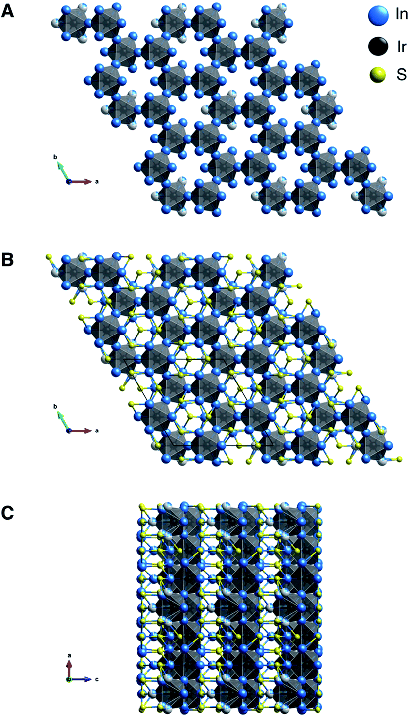 | ||
| Fig. 1 The structure of Ir6In32S21. The space group is the polar, non-centrosymmetric P31m, and the lattice parameters are a = 13.9378(12) Å, c = 8.2316(8) Å, α = β = 90°, γ = 120°. (A) Hexagonal Ir–In network of Ir6In32S21 along the c axis. (B and C) Extended view of Ir6In32S21 along the c axis (B) and the b axis (C). | ||
| a R = Σ‖Fo| − |Fc‖/Σ|Fo|, wR = {Σ[w(|Fo|2 − |Fc|2)2]/Σ[w(|Fo|4)]}1/2 and w = 1/[σ2(Fo2) + (0.0196P)2 + 12.0180P] where P = (Fo2 + 2Fc2)/3. | |
|---|---|
| Empirical formula | Ir6In32S21 |
| Formula weight | 1375.18 |
| Temperature | 298.94 K |
| Wavelength | 0.71073 Å |
| Crystal system | Trigonal |
| Space group | P31m |
| Unit cell dimensions | a = 13.9378(12) Å, α = 90° |
| b = 13.9378(12) Å, β = 90° | |
| c = 8.2316(8) Å, γ = 120° | |
| Volume | 1384.9(3) Å3 |
| Z | 4 |
| Density (calculated) | 6.596 g cm−3 |
| Absorption coefficient | 28.157 mm−1 |
| F(000) | 2366 |
| Crystal size | 0.071 × 0.042 × 0.042 mm3 |
| θ range for data collection | 1.687 to 29.999° |
| Index ranges | −19 ≤ h ≤ 19, −19 ≤ k ≤ 18, −11 ≤ l ≤ 11 |
| Reflections collected | 28![[thin space (1/6-em)]](https://www.rsc.org/images/entities/char_2009.gif) 580 580 |
| Independent reflections | 2843 [Rint = 0.0400] |
| Completeness to θ = 24.957° | 100% |
| Refinement method | Full-matrix least-squares on F2 |
| Data/restraints/parameters | 2843/1/109 |
| Goodness-of-fit | 1.075 |
| Final R indices [I > 2σ(I)] | R obs = 0.0258, wRobs = 0.0691 |
| R indices [all data] | R all = 0.0278, wRall = 0.0704 |
| Extinction coefficient | 0.00012(3) |
| Largest diff. peak and hole | 3.217 and −3.404 e Å−3 |
 | ||
| Fig. 2 (A) Coordination environment around the IrIn7 polyhedron (A). (B) IrIn6 octahedron. Orange bond indicates apical, partially occupied seventh In atom. (C) InIrS3 distorted tetrahedron. (D) Tetrahedral coordination environment of S. Bond lengths for these environments can be seen in Table 2. | ||
| Bond | Length (Å) |
|---|---|
| Ir(1)–In(1) | 2.6212(10) |
| Ir(1)–In(7) | 2.6694(13) |
| Ir(2)–In(5) | 2.6275(10) |
| Ir(2)–In(6) | 2.6674(18) |
| Ir(3)–In(8) | 2.5546(17) |
| Ir(3)–In(9) | 2.600(6) |
| Ir(3)–In(10) | 2.94(4) |
| In(1)–S(1) | 2.605(3) |
| In(1)–S(4) | 2.516(2) |
The honeycomb network is three-dimensional (3D), as the polyhedra are staggered when viewed along the crystallographic b axis. The presence of the distorted octahedron with a partially occupied seventh bond in the honeycomb network is what leads to the polar nature of this compound, as the 3D network does not have an inherent inversion symmetry. The hexagonal network is bridged by In in a distorted tetrahedral coordination (Fig. 2C), where both the S and the Ir are bonding to the In. The distorted tetrahedral coordination environment of the In atoms resembles that of a conventional In1+ in compounds such as InCl.29 The bridging In–S bonds (approximately 2.516(2)–2.605(3) Å) aid in forming an alternating motif, where the honeycomb network and In–S tetrahedra lead into each other and create a 3D structure (Fig. 2D). Notably, Ir forms bonds with In but not with S, likely attributable to the fact that In is the most electropositive atom in the structure. The bonding pattern here is consistent with other subvalent materials, as the In in this material acts as a bridging atom between its more electronegative counterparts.6,9,10
Chemically, the Ir6In32S21 structure has some bonding similarities to other metal-rich structures such as PtIn7F13 and Ru3Sn15O14, as all three are metal-rich subvalent materials with specific transition metal-main group subunits.13,14 Both PtIn7F13 and Ru3Sn15O14 have discrete octahedral subunits, PtIn6 and RuSn6, that are bridged by In–F and Sn–O bonds, respectively. These bonding patterns are like Ir6In32S21 in that IrIn6 and IrIn7 subunits are bridged by In–S bonding. However, the overall structure of Ir6In32S21 is significantly more complex because of the connected 3D hexagonal network of Ir and In along with the alternating structural motifs. Another feature that all three compounds have in common is that they contain electronegative transition metals (Ir, Pt, Ru) and electronegative species (S, F, O) that are bridged by electropositive main group elements (In, Sn). All three compounds have semiconducting behavior with large band gaps, possibly a result of the electron localization on the anionic species that breaks up the polyhedral subunits, an idea that is explored in the optical and electronic structure sections below.
Optical spectroscopy
The UV-Vis Kubelka–Munk transformed diffuse reflectance data (Fig. 3A) shows an absorption edge of 1.48(2) eV. By plotting [(α/S)hν]2 against the photon energy, which is proportional to the Tauc plot analysis for a direct electronic transition, we obtain a straight line which is consistent with the theoretical prediction (see electronic structure section below).30 The band gap is substantially large for a metal-rich chalcogenide material, and because of the localized electron density on the chalcogenide atoms, the gap might be more of an ionic or “salt-like” nature as opposed to a true hybridization gap intermetallic like EuIr4In2Ge4.31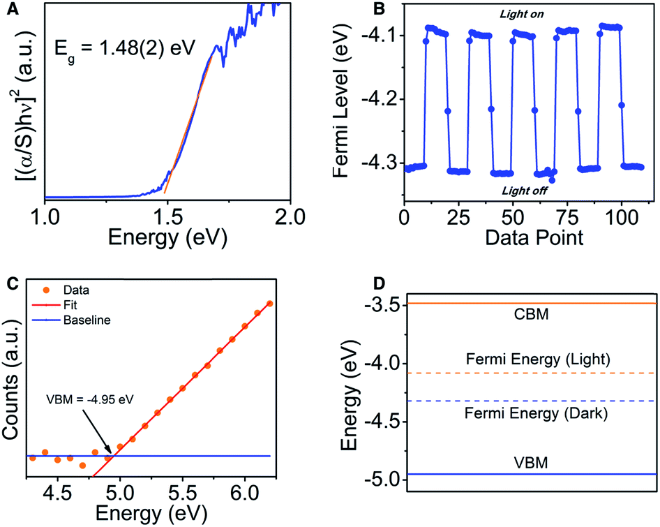 | ||
| Fig. 3 (A) Optical absorption spectrum for Ir6In32S21, showing an absorption edge at 1.48(2) eV. (B) Photo-response of Ir6In32S21, showing a moderate movement of the Fermi level (∼0.2 eV) in response to white light. (C) Ambient photoemission yield spectroscopy, showing the energy of the valence band maximum at −4.95(5) eV. (D) Energy diagram of the VBM, CBM, and Fermi level in the presence and absence of white light. | ||
To further characterize the semiconducting behavior of Ir6In32S21, we utilized Kelvin probe spectroscopy to determine the Fermi level and visible light photo-response of the compound. Kelvin probe spectroscopy is a technique measuring the Fermi level energy at the surface.32 In this technique, a vibrating gold tip is in proximity to but not in contact with the sample, and the contact potential difference (CPD) between the tip and the sample is measured. The CPD is a measure of the Fermi level difference between the sample and the tip. For semiconductors, the Fermi level is located between the top of the valence band and the bottom of the conduction band. For metals, the Fermi level is simply the work function. By measuring the CPD of different metals and comparing it to their work function measured independently by photoemission, the absolute work function of the tip can be calibrated. Knowing the tip work function enables to convert the CPD of the sample into Fermi level in absolute energy values. The Fermi level of the sample was measured both under white light illumination and under dark to show the photo response of the sample. Under illumination, electrons are photo excited into the conduction band, resulting in shifting the Fermi level towards this direction. Ir6In32S21 shows a moderate photo-response of the Fermi energy (∼0.2 eV) in the presence of white light, moving the Fermi level from −4.3 eV to −4.1 eV (Fig. 3B).
We also utilized photoemission yield spectroscopy in air (PYSA) to determine the valence band maximum (VBM) of Ir6In32S21. In PYSA, the sample is illuminated by tunable monochromatic UV light under ambient conditions. A UV photon with energy higher than the VBM, can ionize an electron into the vacuum level. This electron can ionize a gas molecule near the surface which can be measured by the detector. For a typical measurement, the energy of the photons varies between 4.2 eV to 6.2 eV and the number of generated photoelectrons is measured for each energy, while this value is corrected according to the UV lamp spectrum. For semiconductors, the intensity of photoemission near the VBM is generally increases as a cube root of the energy. Hence the cube root of the corrected PYSA spectrum is plotted against the photon energy. The linear region of the plot above the onset is fitted to find the VBM energy, at the crossing of the fit and the background level. The conduction band minimum energy (CBM), is calculated by subtracting the measured band gap from the VBM energy. Based on PYSA measurements, the VBM of Ir6In32S21 was −4.95(5) eV, and the CBM was −3.47(5) eV, further supporting the diffuse reflectance data that Ir6In32S21 is a semiconductor with a notably large band gap (Fig. 3C and D).
XAS data (Fig. 4A and B) were measured to learn about the relative oxidation states and covalency of the Ir and In atoms, with metallic (In, Ir, IrIn2) and semiconducting (In2Se3) materials acting as standards to compare to Ir6In32S21. For the In K-edge data, In metal and Ir6In32S21 have nearly identical absorption edges of 27.9435(1) keV, compared to larger values of 27.9442(1) keV and 27.9445(1) keV for IrIn2 and In2Se3, respectively.33 The Ir L3-edge data are similar, with elemental Ir and Ir6In32S21 having edges of 11.2138(2) and 11.2140(2) keV, respectively, and IrIn2 being slightly larger at 11.2148(2) keV. The absorption edges of Ir6In32S21 are similar to elemental Ir and In in both cases, making an assignment of an oxidation state ambiguous from just these data. We note that XAS absorption edges can have nontrivial differences depending on the electronegativity of the ligand environment around the metal center, indicating that in multiple compounds a metal of interest can have the same oxidation state but substantially different absorption edges depending on its coordination environment.34 To investigate the valence and covalency of S, we also performed X-ray photoelectron spectroscopy (XPS). The data show S 2p3/2 and 2p1/2 binding energies of 161.63 and 162.31 eV, respectively (Fig. 4C). The 2p3/2 value is close to the literature value for In2S3 (161.85 eV), and noticeably lower than elemental S (164.0 eV), suggesting that the S atoms are reduced in a −2 oxidation state, a result that is corroborated by the electronic structure and electron localization function calculations below.35,36 As in the case of the XAS measurements, the core electron binding energies obtained through XPS for both metals lead to inconclusive results as the values obtained are very similar to the values of the pure elements. These XPS data for the Ir and In binding energies can be found in the ESI (Fig. S4†).
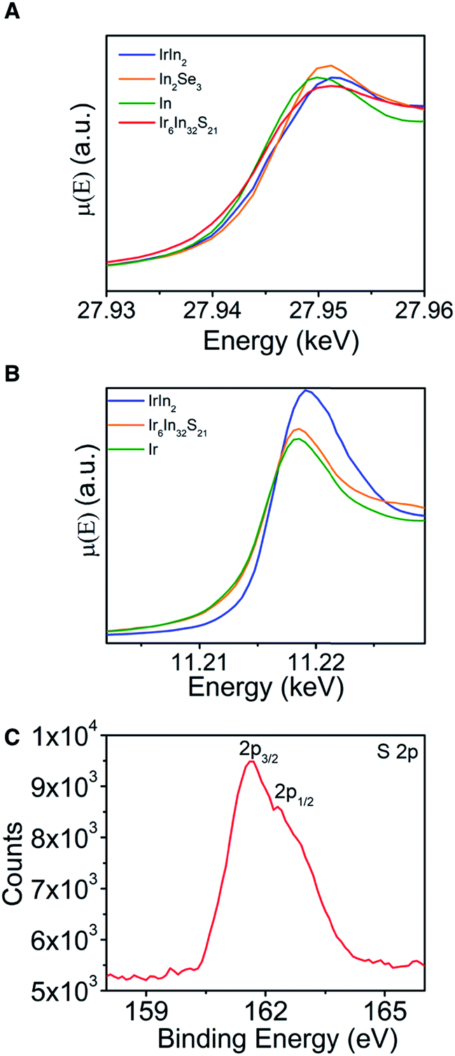 | ||
| Fig. 4 XAS data for (A) In (K-edge) and (B) Ir (L-edge). In both cases, the absorption edges do not clearly indicate an oxidation state for either metal atom. (C) XPS spectrum for the S 2p orbitals. The approximate shifts of the 2p3/2 (161.63 eV) and 2p1/2 (162.31 eV) relative to literature values for In2S3 (161.85 eV) and S (164.0 eV) suggest that the S has been reduced to a −2 oxidation state. | ||
Electronic structure
The electronic band structure (with and without SOC), partial density of states (PDOS), and the crystal orbital Hamilton population (COHP) of Ir6In32S21 can be seen in Fig. 5 (with additional COHP data in Fig. S5†). An Open Quantum Materials Database (OQMD) calculation indicates that Ir6In32S21 is on the convex hull (Fig. S6†). Ir6In32S21 is a nearly direct band gap semiconductor, with the VBM at the Γ point and the CBM along the Γ–A direction. The energy difference between the Γ point and the CBM along the Γ–A is negligible, suggesting that the optical absorption data seen in Fig. 3 is largely the result of a direct transition. The bandwidths of the valence band and conduction band are small at approximately 0.20 and 0.15 eV, respectively. The VBM has hole effective masses of 0.256me, 0.522me, and 2.802me, and the CBM has larger electron effective masses of 1.730me, 1.844me, and 3.959me along the Γ–M, K–Γ, and Γ–A directions, respectively. This is an unusual trend since the effective masses of electrons are generally much lower than those of holes in a conventional semiconductor. The reversal of this trend observed in Ir6In32S21 attests to the unusual bonding character of this material.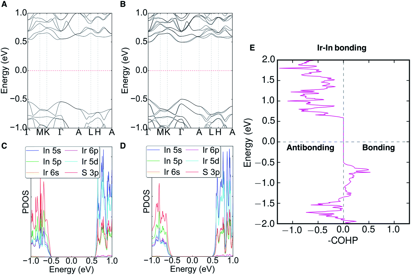 | ||
| Fig. 5 (A and B) Electronic band structure without spin–orbit coupling (SOC) (A) and with SOC (B). (C and D) Partial density of states (PDOS) without SOC (C) and with SOC (D). The PDOS shows that the VBM primarily consists of S 3p orbitals, whereas the CBM is a combination of In 5s and Ir 5d orbitals. (E) Crystal orbital Hamilton population (COHP) of the Ir–In interactions in Ir6In32S21. The COHP indicates that Ir–In interactions are bonding in the valence band and antibonding in the conduction band. | ||
The PDOS shows that the VBM is comprised primarily of S 3p orbitals and the CBM can be attributed to the In 5s (In3+) and Ir 5d (eg) orbitals. The strong hybridization between In 5s and Ir 5d orbitals leads to less dispersive conduction bands. The polar crystal structure causes the bands to have noticeable Dresselhaus spin-splitting at the Γ point because of the strong SOC effects of the Ir atoms, with a ΔSOC ∼0.03 eV relative to the band structure without SOC. The polar nature of the P31m space group would also permit Rashba spin-splitting to occur in the compound, but it is not noticeable in the band structure, as the splitting only results in changes in energy (Dresselhaus effect) as opposed to changes in the wave vector (Rashba effect).37 The COHP analysis of the Ir–In interactions shows bonding character near the valence band edge and strongly antibonding character all along the conduction band. The COHP for the VBM is consistent with the relatively short Ir–In bond lengths mentioned above, suggesting that Ir6In32S21 may have stronger bonds than its intermetallic counterparts (e.g. IrIn2 and IrIn3).
The origin of the energy gap in Ir6In32S21 is likely a result of electron transfer from the metal atoms (particularly the In 5s electrons) to the more electronegative S atoms. This suggests that the bridging In–S bonds between the Ir–In honeycomb networks lead to the overall semiconducting behavior of the compound. The electron localization function (ELF), seen in Fig. 6, corroborates this idea, where the red regions correspond to areas of high electron density in the structure and the blue regions indicate almost no electron density. The ELF is consistent with the PDOS in that the S 3p atoms are the filled states, with a strong degree of localized electron density on these atoms. The In atoms, in turn, have almost no electron density, which is attributable to the fact that they are significantly less electronegative than either S or Ir and are donating their electron density in this structure. The Ir atoms appear to also have an intermediate amount of electron density, indicating that there is a degree of delocalized electron density around them consistent with their higher electronegativity.
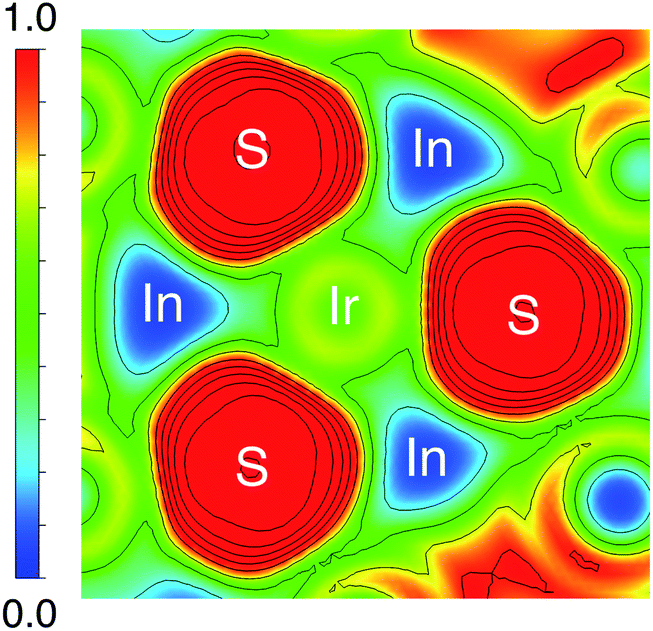 | ||
| Fig. 6 ELF plot of a two-dimensional cut of Ir6In32S21 along the ab plane. The red regions indicate high electron density, and the blue regions indicate negligible electron density. The ELF analysis suggests that electron density is localized heavily on the S atoms, along with moderate electron density around the Ir atoms. The In atoms surrounding the Ir and S are nearly electron deficient in comparison, consistent with electron transfer from In to S and Ir. | ||
The localization function, band structure, and COHP results suggest the bonding character is in the middle of the spectrum between metallic and semiconducting, with strong degrees of salt-like electron localization on the chalcogenide atoms contrasting with the dearth of electron density between the short Ir–In bonds. In this case, it is likely that the strong electron localization on the S atoms is the dominant force in its bonding character, leading to its overall semiconducting behavior. Although having ionic and metallic regions are common in metal-rich materials with main group elements (e.g. chalcogenides and halides), it is still notable that Ir6In32S21 has such a large band gap, as most of these materials tend to behave as confined metals.4,38 It is possible that the alternating motif of the structure breaks up any potential metallicity the hexagonal network might have, similar to PtIn7F13, Ru3Sn15O14, and the topological insulator Bi14Rh3I9.9,13,14
Conclusion
Ir6In32S21 is a novel metal-rich polar semiconducting subchalcogenide with a band gap of 1.48(2) eV. The In metal flux enables the stabilization of this material, allowing for large crystals to be easily grown. The material exhibits a photoresponse of ∼0.2 eV shift in the Fermi level in the presence of white light and DFT calculations suggest the existence of Dresselhaus spin-splitting. The energy gap in this compound is the result of electron transfer from the Ir and In atoms to the S atoms, corroborated by the PDOS and ELF calculations. XPS indicates a −2 oxidation state for the S atoms. The lack of clearly defined oxidation states from the metallic elements is like other subchalcogenide and subhalide materials. Ir6In32S21 provides the additional insight that extended metal–metal bonded networks can still lead to semiconducting behavior, and is a good platform for exploring the origin of semiconducting behavior in subvalent materials.Experimental methods
Synthesis
All reagents were used as obtained: Ir powder (99.5%, American Elements), In teardrops (99.999%, Plasmaterials), and sulfur pieces (99.998%, Sigma Aldrich). To synthesize Ir6In32S21, Ir (0.5 mmol, 0.0961 g), S (2 mmol, 0.0652 g), and excess In (20 mmol, 2.2964 g) were loaded into an alumina crucible. A 100-mesh stainless steel filter was placed on top of the crucible, with another piece of alumina tubing placed on top of the filter to act as a counterweight. The crucible, 100-mesh filter, and alumina tubing were all loaded into an 18 mm fused silica tube and flame sealed under vacuum at ∼3 × 10⁻³ mbar. Once the tube was sealed, divots were placed into the tube above the alumina tubing with the torch to hold the setup in place. The tube was placed into a programmable furnace and heated to 1000 °C in 12 h, held there for 24 h, and cooled to 650 °C in 24 h, after which the tube was removed at that temperature from the furnace and immediately centrifuged to remove excess In flux. To remove residual In on the surface of the Ir6In32S21 crystals, they were placed in dilute HCl (10–12 wt%) for 2–3 h, and filtered and washed with water and acetone. The crystals are air stable and remain stable in dilute HCl solution for at least 2–3 days. Yield for these In flux reactions range from ∼50–70% depending on the limiting reagent.Single crystal X-ray diffraction
Single crystals of Ir6In32S21 were adhered to a glass fiber with super glue. Single crystal X-ray diffraction was performed at 299 K on a Bruker-Apex II CCD diffractometer with Mo Kα radiation (λ = 0.71073 Å). The data were integrated using SAINT v-8.38A and a multi-scan absorption correction was applied using the program SADABS.39 The structure was solved by the SHELXT software package using intrinsic phasing, and refined with SHELXL by the least squares method.40 The crystallographic information and selected bond lengths can be found in Tables 1 and 2, respectively, and additional crystallographic information can be found in the ESI.†Density functional theory (DFT) calculations
All density functional theory (DFT) calculations are performed using the projector augmented wave (PAW) method, as implemented in the Vienna ab initio Simulation Package (VASP).41–44 The Perdew–Burke–Ernzerhof (PBE) exchange–correlation functional, a plane wave basis set with a cutoff energy of 520 eV, and a Γ-centered 4 × 4 × 9 k-mesh for sampling the Brillouin zone were used for electronic structure calculations.45 The COHP analysis was performed by using the LOBSTER code based on DFT wave functions.27,46 The electron localization function was calculated after full atomic relaxation of the structure.Solid state UV-Vis spectroscopy
Optical diffuse reflectance measurements were performed from the 2500–250 nm range at room temperature using a Shimadzu UV-3600 PC double-beam, double-monochromator spectrophotometer. BaSO4 was used as the standard for diffuse reflectance, and it was set to 100% reflectance. Powders of Ir6In32S21 were pressed into the BaSO4 standard for the measurement. The reflectance data was converted into absorbance using the Kubelka–Munk equation: α/S = (1 − R)2/2R, where R is reflectance, α is the absorption coefficient, and S is the scattering coefficient.30X-ray absorption spectroscopy (XAS)
Transmission mode X-ray absorption spectroscopy (XAS) experiments were carried out, using the sector-20 bending magnet beamline at the Advanced Photon Source (APS) of Argonne National Laboratory (APS), at the Ir L3- and In K-edges. The incident beam was monochromatized using a fixed exit Si (111) monochromator. Harmonic contamination was minimized by crystal detuning for the In edge and by using a rhodium-coated mirror at the Ir edge. The intensity of the incident and transmitted beams were measured using gas-ionization chambers using the appropriate inert gas mixtures. The energy calibration was monitored using In foil and Ir powder standard as reference. All samples were prepared as cold pressed pellets by mixing an appropriate amount of sample with dry hexagonal BN as a binder. XAS data were processed and analyzed using Athena, a part of the Demeter 0.9.26 software package.47X-ray photoelectron spectroscopy (XPS)
XPS data were collected using a Thermo Scientific ESCALAB 250 Xi spectrometer. To approximate the bulk crystal as opposed to the surface, depth profiles were performed by ion milling with Ar+ ions to etch ∼50 nm into the crystal. Additional Ir and In XPS data (Ir 4d and 4f, In 3p and 3d) can be found in the ESI.†Photoemission yield spectroscopy in air (PYSA)
The valence band maximum energy (VBM) of a Ir6In32S21, was measured by Photoemission yield spectroscopy in air (PYSA, AC-2, Riken-Keiki). Briefly, the sample is scanned by tunable monochromatic ultraviolet light (UV, 4.2–6.2 eV), under ambient conditions and the number of generated photoelectrons are measured at each excitation energy. Photoelectrons are only generated when the photon energy is higher than the VBM. The VBM is determined by finding the onset of the PYSA spectra.Kelvin probe spectroscopy
The Fermi level energy was measured by Kelvin probe spectroscopy (KP, APS04, KP Technology). In this measurement, the contact potential difference (CPD) is measured between the sample and a vibrating gold tip. The CPD is a measure of the Fermi level difference between the sample and the tip, and was calibrated using gold and silver standards. The Fermi level of the sample was measured under white light illumination (xenon lamp, 150 W) and under dark to measure the photo-response of the Fermi level.Conflicts of interest
The authors declare no conflicts of interest.Acknowledgements
This work was supported by the National Science Foundation (NSF) grant DMR-1708254 (synthesis and structural characterization). PYSA and KP measurements were carried out with equipment acquired by ONR grant N00014-18-1-2102. Single crystal diffraction data was performed at the IMSERC facility at Northwestern University, which has received support from the Soft and Hybrid Nanotechnology Experimental (SHyNE) Resource (NSF NNCI-1542205); the State of Illinois; and International Institute for Nanotechnology (IIN). This research used resources of the Advanced Photon Source (APS), a U.S. Department of Energy (DOE) Office of Science User Facility operated for the DOE Office of Science by Argonne National Laboratory under Contract No. DE-AC02-06CH11357. The work for DFT calculations carried out by J. E. P., J. H., and C. W. was supported by the U.S. Department of Energy, Office of Science Basic Energy Sciences grant DE-SC0014520. The NLO measurements were supported by AFOSR Grant FA9550-19-1-0243 (V. G., M. G. K.). We also acknowledge QUEST, a supercomputer facility at Northwestern University and resources of the National Energy Research Scientific Computing Center (NERSC), a U.S. Department of Energy Office of Science User Facility operated under Contract No. DE-AC02-05CH11231. R. Z. and V. G. acknowledge support from the NSF grant number DMR-1807768 and NSF-MRSEC Penn State Center for Nanoscale Science, grant number DMR-1420620. We thank Dr Kyle M. McCall and Tyler J. Slade for insightful discussions.References
- M. G. Kanatzidis, Inorg. Chem., 2017, 56, 3158–3173 CrossRef CAS PubMed.
- M. G. Kanatzidis, R. Pöttgen and W. Jeitschko, Angew. Chem., Int. Ed., 2005, 44, 6996–7023 CrossRef CAS PubMed.
- T. Graf, C. Felser and S. S. P. Parkin, Prog. Solid State Chem., 2011, 39, 1–50 CrossRef CAS.
- J. D. Corbett, Inorg. Chem., 2010, 49, 13–28 CrossRef CAS PubMed.
- J. D. Corbett, Angew. Chem., Int. Ed., 2000, 39, 670–690 CrossRef CAS PubMed.
- M. Ruck, Angew. Chem., Int. Ed., 2001, 40, 1182–1193 CrossRef CAS PubMed.
- M.-H. Whangbo, C. Lee and J. Köhler, Eur. J. Inorg. Chem., 2011, 2011, 3841–3847 CrossRef CAS.
- T. Sakamoto, M. Wakeshima, Y. Hinatsu and K. Matsuhira, Phys. Rev. B: Condens. Matter Mater. Phys., 2007, 75, 060503 CrossRef.
- B. Rasche, A. Isaeva, M. Ruck, S. Borisenko, V. Zabolotnyy, B. Büchner, K. Koepernik, C. Ortix, M. Richter and J. van den Brink, Nat. Mater., 2013, 12, 422 CrossRef CAS PubMed.
- M. Ruck, Z. Kristallogr. - Cryst. Mater., 2010, 225, 167 CAS.
- M. Ruck, Z. Anorg. Allg. Chem., 1995, 621, 2034–2042 CrossRef CAS.
- J. F. Khoury, A. J. E. Rettie, M. A. Khan, N. J. Ghimire, I. Robredo, J. E. Pfluger, K. Pal, C. Wolverton, A. Bergara, J. S. Jiang, L. M. Schoop, M. G. Vergniory, J. F. Mitchell, D. Y. Chung and M. G. Kanatzidis, J. Am. Chem. Soc., 2019, 141, 19130–19137 CrossRef CAS PubMed.
- W. Reichelt, T. Söhnel, O. Rademacher, H. Oppermann, A. Simon, J. Köhler and H. Mattausch, Angew. Chem., Int. Ed., 1995, 34, 2113–2114 CrossRef CAS.
- J. Köhler and J.-H. Chang, Angew. Chem., Int. Ed., 2000, 39, 1998–2000 CrossRef.
- J. Köhler, R. Dinnebier, H. A. Friedrich and A. Fitch, Z. Anorg. Allg. Chem., 2014, 640, 3172–3176 CrossRef.
- P. S. Halasyamani and K. R. Poeppelmeier, Chem. Mater., 1998, 10, 2753–2769 CrossRef CAS.
- L. M. Schoop, F. Pielnhofer and B. V. Lotsch, Chem. Mater., 2018, 30, 3155–3176 CrossRef CAS.
- G. Dresselhaus, Phys. Rev., 1955, 100, 580–586 CrossRef CAS.
- S. D. Ganichev and L. E. Golub, Phys. Status Solidi B, 2014, 251, 1801–1823 CrossRef CAS.
- X. Zhang, Q. Liu, J.-W. Luo, A. J. Freeman and A. Zunger, Nat. Phys., 2014, 10, 387 Search PubMed.
- A. Nuber, J. Braun, F. Forster, J. Minár, F. Reinert and H. Ebert, Phys. Rev. B: Condens. Matter Mater. Phys., 2011, 83, 165401 CrossRef.
- P. D. C. King, R. C. Hatch, M. Bianchi, R. Ovsyannikov, C. Lupulescu, G. Landolt, B. Slomski, J. H. Dil, D. Guan, J. L. Mi, E. D. L. Rienks, J. Fink, A. Lindblad, S. Svensson, S. Bao, G. Balakrishnan, B. B. Iversen, J. Osterwalder, W. Eberhardt, F. Baumberger and P. Hofmann, Phys. Rev. Lett., 2011, 107, 096802 CrossRef CAS PubMed.
- I. Žutić, J. Fabian and S. Das Sarma, Rev. Mod. Phys., 2004, 76, 323–410 CrossRef.
- S. Parkin, J. Xin, C. Kaiser, A. Panchula, K. Roche and M. Samant, Proc. IEEE, 2003, 91, 661–680 CrossRef CAS.
- S. A. Wolf, D. D. Awschalom, R. A. Buhrman, J. M. Daughton, S. von Molnár, M. L. Roukes, A. Y. Chtchelkanova and D. M. Treger, Science, 2001, 294, 1488 CrossRef CAS PubMed.
- D. D. Awschalom and M. E. Flatté, Nat. Phys., 2007, 3, 153 Search PubMed.
- S. Maintz, V. L. Deringer, A. L. Tchougréeff and R. Dronskowski, J. Comput. Chem., 2016, 37, 1030–1035 CrossRef CAS PubMed.
- S. A. Denev, T. T. A. Lummen, E. Barnes, A. Kumar and V. Gopalan, J. Am. Ceram. Soc., 2011, 94, 2699–2727 CrossRef CAS.
- J. M. van den Berg, Acta Crystallogr., 1966, 20, 905–910 CrossRef CAS.
- J. H. Liao, C. Varotsis and M. G. Kanatzidis, Inorg. Chem., 1993, 32, 2453–2462 CrossRef CAS.
- N. P. Calta, J. Im, A. P. Rodriguez, L. Fang, D. E. Bugaris, T. C. Chasapis, A. J. Freeman and M. G. Kanatzidis, Angew. Chem., Int. Ed., 2015, 54, 9186–9191 CrossRef CAS PubMed.
- M. M. Beerbom, B. Lägel, A. J. Cascio, B. V. Doran and R. Schlaf, J. Electron Spectrosc. Relat. Phenom., 2006, 152, 12–17 CrossRef CAS.
- S. Kraft, J. Stümpel, P. Becker and U. Kuetgens, Rev. Sci. Instrum., 1996, 67, 681–687 CrossRef CAS.
- G. M. Dalpian, Q. Liu, C. C. Stoumpos, A. P. Douvalis, M. Balasubramanian, M. G. Kanatzidis and A. Zunger, Phys. Rev. Mater., 2017, 1, 025401 CrossRef.
- B. J. Lindberg, K. Hamrin, G. Johansson, U. Gelius, A. Fahlman, C. Nordling and K. Siegbahn, Phys. Scr., 1970, 1, 286–298 CrossRef CAS.
- Y. Tao, A. Yelon, E. Sacher, Z. H. Lu and M. J. Graham, Appl. Phys. Lett., 1992, 60, 2669–2671 CrossRef CAS.
- Q. Liu, X. Zhang, H. Jin, K. Lam, J. Im, A. J. Freeman and A. Zunger, Phys. Rev. B: Condens. Matter Mater. Phys., 2015, 91, 235204 CrossRef.
- L. Chen and J. D. Corbett, J. Am. Chem. Soc., 2003, 125, 1170–1171 CrossRef CAS PubMed.
- SAINT, version 8.38A, Bruker Analytical X-ray Instruments, Inc., Madison, WI., 2008 Search PubMed.
- G. M. Sheldrick, SHELXTL, version 6.14, Bruker Analytical X-ray Instruments, Inc., Madison, WI., 2003 Search PubMed.
- G. Kresse and J. Furthmüller, Phys. Rev. B: Condens. Matter Mater. Phys., 1996, 54, 11169–11186 CrossRef CAS PubMed.
- G. Kresse and D. Joubert, Phys. Rev. B: Condens. Matter Mater. Phys., 1999, 59, 1758–1775 CrossRef CAS.
- P. E. Blöchl, Phys. Rev. B: Condens. Matter Mater. Phys., 1994, 50, 17953–17979 CrossRef PubMed.
- G. Kresse and J. Furthmüller, Comput. Mater. Sci., 1996, 6, 15–50 CrossRef CAS.
- J. P. Perdew, K. Burke and M. Ernzerhof, Phys. Rev. Lett., 1996, 77, 3865–3868 CrossRef CAS PubMed.
- V. L. Deringer, A. L. Tchougréeff and R. Dronskowski, J. Phys. Chem. A, 2011, 115, 5461–5466 CrossRef CAS PubMed.
- B. Ravel and M. Newville, Phys. Scr., 2005, 1007, DOI:10.1238/physica.topical.115a01007.
Footnote |
| † Electronic supplementary information (ESI) available. CCDC 1963929. For ESI and crystallographic data in CIF or other electronic format see DOI: 10.1039/c9sc05609b |
| This journal is © The Royal Society of Chemistry 2020 |