
 Open Access Article
 This Open Access Article is licensed under a Creative Commons Attribution-Non Commercial 3.0 Unported Licence
III–V colloidal nanocrystals: control of covalent surfaces
Youngsik
Kim†
 a,
Jun Hyuk
Chang†
b,
Hyekyoung
Choi
a,
Yong-Hyun
Kim
c,
Wan Ki
Bae
*d and
Sohee
Jeong
*a
a,
Jun Hyuk
Chang†
b,
Hyekyoung
Choi
a,
Yong-Hyun
Kim
c,
Wan Ki
Bae
*d and
Sohee
Jeong
*a
aDepartment of Energy Science, Center for Artificial Atoms, Sungkyunkwan University, Suwon-si, Gyeonggi-do 16419, Republic of Korea. E-mail: s.jeong@skku.edu
bSchool of Chemical and Biological Engineering, Seoul National University, Seoul, Republic of Korea
cGraduate School of Nanoscience and Technology, Department of Physics, Korea Advanced Institute of Science and Technology, Daejeon 34141, Republic of Korea
dSKKU Advanced Institute of Nanotechnology (SAINT), Center for Artificial Atoms, Sungkyunkwan University, Suwon-si, Gyeonggi-do 16419, Republic of Korea. E-mail: wkbae@skku.edu
First published on 26th November 2019
Abstract
Colloidal quantum dots (QDs) are nanosized semiconductors whose electronic features are dictated by the quantum confinement effect. The optical, electrical, and chemical properties of QDs are influenced by their dimensions and surface landscape. The surface of II–VI and IV–VI QDs has been extensively explored; however, in-depth investigations on the surface of III–V QDs are still lagging behind. This Perspective discusses the current understanding of the surface of III–V QDs, outlines deep trap states presented by surface defects, and suggests strategies to overcome challenges associated with deep traps. Lastly, we discuss a route to create well-defined facets in III–V QDs by providing a platform for surface studies and a recently reported approach in atomistic understanding of covalent III–V QD surfaces using the electron counting model with fractional dangling bonds.
 Youngsik Kim | Youngsik Kim is a PhD student at the Department of Energy Science, Sungkyunkwan University in South Korea. His research interests include the synthesis and surface chemistry of quantum confined nanocrystals for use in light emitting diodes and photovoltaics. |
 Jun Hyuk Chang | Jun Hyuk Chang is a PhD candidate at Seoul National University, South Korea. He received a B.S. degree in 2015 from the same university. His research interests include the synthesis and characterization of nanocrystal quantum dots for use in light-emitting diodes. |
 Hyekyoung Choi | Hyekyoun Choi is a research professor at the Department of Energy Science, Sungkyunkwan University (SKKU). She received her PhD in Nanomechatronics from the University of Science and Technology (UST) in South Korea in 2017. Her research interests include synthesis and surface chemistry of colloidal nanocrystals for high performance opto-electronic devices. |
 Yong-Hyun Kim | Prof. Yong-Hyun Kim is currently a tenured professor at the Graduate School of Nanoscience and Technology and the Department of Physics, KAIST. He received his B.S. (1997), M.S. (1999), and PhD (2003) from the Department of Physics, KAIST and worked for National Renewable Energy Laboratory, Golden, Colorado, USA as a post-doc and regular staff scientist from 2003 to 2009. His current research projects are associated with computational materials physics for energy storage and utilization. |
 Wan Ki Bae | Wan Ki Bae is an assistant professor at SAINT, Sungkyunkwan University (SKKU). He received his B.S., M.S., and PhD Chemical and Biological Engineering degrees from Seoul National University (SNU) in South Korea in 2003, 2005, and 2009, respectively. He conducted postdoctoral study at Los Alamos National Laboratory in 2010–2013 and was a senior researcher at the Korea Institute of Science and Technology (KIST) in 2013–2018 before he joined the faculty of SKKU in 2018. |
 Sohee Jeong | Sohee Jeong is currently an associate professor at the Department of Energy Science of Sungkyunkwan University (SKKU). Before joining SKKU, she was a principal researcher at the Korea Institute of Machinery and Materials (KIMM). She obtained her B.S. and M.S. Chemistry degrees from the Korea Advanced Institute of Science and Technology (KAIST) and her PhD Chemistry degree from the University of Michigan in Ann Arbor, MI, USA. Her current research interests include the microscopic understanding of the surface chemistry of nanocrystal quantum dots, specifically aiming at efficient charge transfer for quantum-dot-based applications, including photovoltaics. |
1. Introduction
Colloidal quantum dots (QDs), whose photophysical properties vary depending upon their dimension, are considered to be the most promising candidates for a variety of applications including displays,1,2 photovoltaics,3–9 and biomarkers.10–12 Since 10–70% of the total number of atoms reside at the exterior of nanometer sized QDs, the impact of the QD surface on its photophysical and electrical properties is substantial.13 Hence, understanding and controlling the QD surface has been a central theme in QD research.Among the various binary QDs that have been explored, III–V QDs have attracted considerable attention because they do not contain toxic elements (e.g., Cd or Pb) that are strictly regulated in commercial use.13,14 More importantly, III–V QDs are expected to exhibit unprecedented photophysical properties that cannot be easily obtained with II–VI or IV–VI QDs.15–18 Their relative covalent crystal bonding nature also imparts chemical robustness in polar environments.
As observed in II–VI and IV–VI QDs,19–23 control over the surface of III–V QDs is prerequisite to fully exploit them in optoelectronic applications. The ability to accurately implement the bandgap24 and display tunable electronic energy level positions8,25,26 through modulation of particle size and surface ligands, respectively, are requisite characteristics of high performance III–V QDs. Exciton dynamics can also be engineered into the QDs by controlling the shape or heterostructure formation. This can be achieved by controlling the reactivity of precursors or the synthesis process to enable diffusion-controlled growth.14,34–37
Herein, we present perspectives of research on III–V QDs focusing on their surface properties (Fig. 1). Specifically, in regard to studies on surface chemistry for high performance III–V QDs, we discuss the challenges in achieving ideal optoelectronic properties that originate from un-controlled covalent III–V QD surfaces, such as the deep trap states caused by surface defects.38,39 Then, approaches on eliminating deep trap states, including semiconducting shell growth over the core40 surface etching of dangling atoms,41 and post-synthetic ligand passivation,42,43 are reviewed. The size-dependent faceted QD model and related facet-dependent surface chemistry that are well established in IV–VI QDs are revisited to facilitate an understanding of the surface properties of III–V QDs. Finally, the electron counting model with fractional dangling bonds44 is introduced as a tool to view the surface of III–V QDs in atomistic detail.
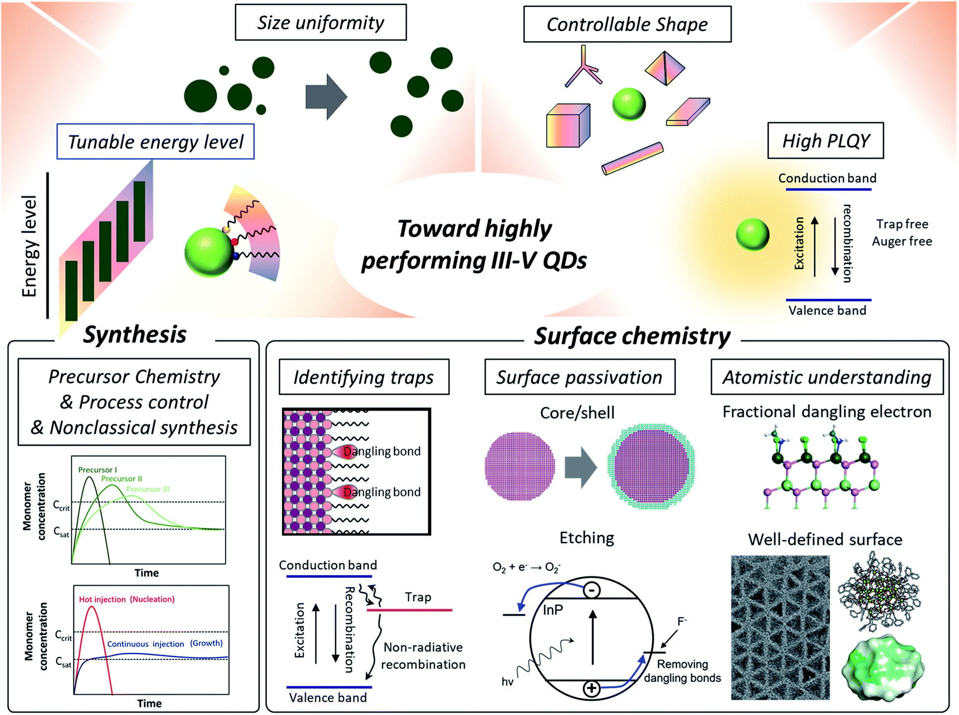 | ||
| Fig. 1 Towards high performance III–V QDs. High performance QDs require tunable energy levels, size uniformity, controllable shape, and high photoluminescence quantum yields. Synthetic approaches include developing new molecular precursors with controlled reactivity or processing control for induced focusing during the growth. Non-classical growth mechanisms are currently being explored for better control of III–V QD synthesis. In regard to surface chemistry, which is the focus of this perspective, research on identifying the origin of trap states is reviewed. Two prevailing ways to passivate surface traps of III–V QDs are removing dangling bonds via a core/shell approach and etching. Having an atomistic surface structure of III–V QDs using synthetic design and density functional theory (DFT) based surface energy calculations is beneficial for developing precisely controlled passivation approaches, as evidenced from IV–VI QDs. The atomistic description of fractional dangling electrons is reproduced with permission from ref. 44. Copyright 2017 Royal Society of Chemistry. The TEM image of tetrahedron shaped InP nanocrystals is reproduced with permission from ref. 88. Copyright 2016 Wiley Online Library. The molecular structure of InP nanoclusters which have a well-defined number of atoms with their surface energy map is reproduced with permission from ref. 85 and 86. Copyright 2016, 2018 American Chemical Society. | ||
2. Characteristics and challenges of III–V QDs
Lattice covalency can be evaluated using Phillips ionicity (f), which represents the quantified values of the chemical bonding tendency between ionic and covalent bonding. Generally, III–V semiconductors have a smaller Phillips ionicity, and thus they have relatively larger lattice covalency (e.g., f of InP and CdS equals 0.421 and 0.685, respectively).30,45 This lattice covalency of III–V materials affects various physical and chemical properties. For example, covalent-bonding characteristics, representing delocalization of electron wavefunction across constituent chemical elements, give rise to a smaller effective mass of the electrons and a larger dielectric constant of the materials.38Table 1 lists the basic parameters of representative bulk III–V semiconductors. On account of their electronic properties27,29,30,46 with robustness under electric or environmental stress that cannot be addressed easily with II–VI or IV–VI semiconductors, III–V semiconductors are widely used in optoelectronic applications.
| Materiala | GaP | GaAs | GaSb | InP | InAs | InSb |
|---|---|---|---|---|---|---|
a All materials are zinc blende structures.
b Mass values are obtained by cyclotron resonance.27
c Exciton Bohr radius, aexc, is calculated using 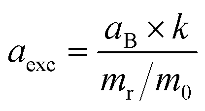 ref. 28. aB is the Bohr radius of the hydrogen atom, k is the dielectric constant of the material, mr is the reduced effective mass, and m0 is the free electron mass.
d The mobility values at 300 K are obtained under clean conditions, so that the impurities and structural defects influence their mobility.
e
Ref. 29.
f
Ref. 27.
g
Ref. 30.
h
Ref. 31.
i
Ref. 32.
j
Ref. 33. ref. 28. aB is the Bohr radius of the hydrogen atom, k is the dielectric constant of the material, mr is the reduced effective mass, and m0 is the free electron mass.
d The mobility values at 300 K are obtained under clean conditions, so that the impurities and structural defects influence their mobility.
e
Ref. 29.
f
Ref. 27.
g
Ref. 30.
h
Ref. 31.
i
Ref. 32.
j
Ref. 33.
|
||||||
| Bandgap typef | Indirect | Direct | Direct | Direct | Direct | Direct |
| Ionicity (Philips)g | 0.374 | 0.31 | 0.261 | 0.421 | 0.357 | 0.321 |
| Ionicity (Pauling)g | 0.27 | 0.26 | 0.26 | 0.26 | 0.26 | 0.25 |
| Effective mass of electron (me/m0)b,f | 0.21e | 0.067 | 0.042 | 0.077 | 0.023 | 0.014 |
| Effective mass of light hole (mlh/m0)b,f | 0.17e | 0.082 | 0.047 | 0.12 | 0.026 | 0.021 |
| Effective mass of heavy hole (mhh/m0)b,f | 0.67e | 0.45 | 0.26 | 0.56 | 0.35 | 0.45 |
| Bandgap at 300 K (eV)f | 2.272 | 1.424 | 0.725 | 1.344 | 0.356 | 0.180 |
| Lattice constant (Å)e | 5.45 | 5.65 | 6.09i | 5.86 | 6.05 | 6.47 |
| Exciton Bohr radius (nm)c | 7.3e | 11.5 | 23.4 | 9.8 | 35.9 | 61.7 |
| Electron mobility (cm2 V−1 s−1) at 300 Kd,f | 190 | 9750 | 7700 | 5400 | 33![[thin space (1/6-em)]](https://www.rsc.org/images/entities/char_2009.gif) 000 000 |
77000 |
| Hole mobility (cm2 V−1 s−1) at 300 Kd,f | 150 | 450 | 1000 | 150 | 450 | 850 |
| Dielectric constantf | 10.7h | 12.6 | 15.7 | 12.4 | 14.6 | 15.7j |
For instance, GaN enables stable and efficient blue light-emitting diodes,47 and GaAs enables the highest efficiency single-junction solar cells (29.1% according to the NREL chart, 2019).48 However, the excellent properties that are prevalent in bulk III–V semiconductors rarely appear in colloidal QDs, mainly due to the difficulty in controlling the colloidal synthesis and the surface properties of III–V QDs.38 Typically, epitaxial growth of III–V crystals (e.g., GaAs, InP, and GaSb) requires reaction temperatures ranging from 520 to 800 °C, which is much higher than the temperature that is required for II–VI materials (250–450 °C).49 To grow III–V crystals in solution, the use of highly reactive precursors that constrain the process window for QD synthesis is inevitable.38,45 There have been numerous attempts to find suitable precursor reactivities and process conditions based on classical and non-classical nucleation and growth models.14,50,51 Synthesis using a metal–carboxylate ligand and tris(trimethylsilyl)pnictogen ((TMS)3V) as the precursor is most widely explored for III–V QD synthesis as thoroughly covered in great detail in several reviews.14,45,52–54 The defects that rarely appear in ionic-bonding compound QDs should be considered for III–V QDs with a strong covalent lattice. In addition to the synthetic challenges of high quality III–V QDs, passivation of the surface is another, yet more critical, issue.38,39,41 The electronic energy level of trap states that originate from broken bonds at the surface atoms of III–V QDs resides much deeper when compared with the case of ionic-bonding characteristics.38,55 Heath and Shiang demonstrated that the surface trap energies of similarly sized QDs are significantly different for CdSe and InP QDs (0.25 and 6.3 kJ mol−1 for 30 Å CdSe and InP QDs, respectively).38 To identify the origin of deep trap states, Fu et al. calculated the trap states of InP QDs via the semi-empirical pseudopotential method.39 According to their calculations, InP QDs do not hold trap states inside the bandgap when their surfaces are completely passivated. In other words, the deep trap states in the bandgap originate from surface defects. When the particle size of InP QDs is 4 nm, the trap depth of the P dangling bond and the valence band edge is 0.42 eV, while the trap depth of the In dangling bond and the conduction band edge is relatively small value of 0.08 eV (Fig. 2a and b), indicating that the P dangling bond in InP QDs is responsible for deep trap states. More recently, based on cluster model calculations that exclude one-dimensional confinement errors,56 the indium dangling bond has been considered to be responsible for deep trap states, especially in QDs with small particle sizes. Indium and phosphorous dangling bonds generate deep trap states at −3.947 eV and shallow trap states at −5.717 eV, respectively. Note that in the case of InP QDs, the conduction band edge energy level is affected to a greater extent than the valence band edge energy level upon variation of the QD volume, following their respective effective mass.56,57 Therefore, electron trap energies become greater for smaller InP QDs.56 Additionally, in the case of GaAs QDs, the structural defect of a Ga vacancy and lattice disorder is speculated to be responsible for their indirect-like optical properties.58 Structural defects that barely appear in ionic-bonding compound QDs should be taken into account for III–V QDs with a strong covalent lattice.
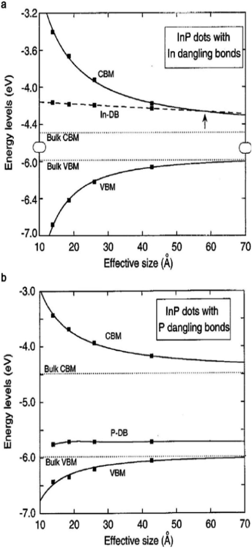 | ||
| Fig. 2 Energy level of (a) indium dangling bonds (DB), size dependent conduction band minimum (CBM), and valence band maximum (VBM) of InP QDs. The arrow indicates the size for which the energy state of the dangling bond appears. (b) P dangling bonds in InP QDs. Reproduced with permission from ref. 39. Copyright 1997 The American Physics Society. | ||
In addition, III–V QDs suffer from severe oxidation upon exposure to any oxygen sources, owing to the high oxophilicity of elements in groups III and V.59–61 Although the effect of surface oxidation on the optical properties of III–V QDs is still largely un-explored, it is apparent that the oxidized surface obscures atomistic surface investigations. An oxidation-free surface will certainly facilitate a greater understanding of the surface of III–V QDs.
Approaches to passivate the surface of III–V QDs, such as inorganic shelling on the core and etching off the dangling bonds, are discussed in the next section.
3. Surface passivation
3.1 Core/shell formation
Growing inorganic layers with similar crystal structures is the most prevalent strategy to passivate the surface defects of QDs. Inorganic passivation layers with a larger bandgap spatially decouple the electron and hole wavefunctions sitting at the core from the surface trap states, leading to the enhancement of both luminescence efficiency and photochemical stability of QDs. Initially, the heterostructured QDs started from a rather simple architecture (e.g., CdSe/ZnS62) and have evolved to equip with more complex architectures.The state-of-the-art heterostructured QDs retain delicately engineered thick shells to mitigate structural stresses between the core and shell materials (e.g., multiple alloy or composition gradient shells) for high luminescence efficiency even under thermal stresses or electrical fields.63–66
The protocol for core/shell heterostructuring, which has been successfully employed in QDs with ionic bonding characteristics, has been applied to III–V QDs.67–69 The first demonstration was a InP/ZnS core/shell heterostructure.70 The growth of a thin ZnS layer (∼1 nm) effectively passivates the surface trap states on the InP surface, enabling a high luminescence efficiency (photoluminescence quantum yield ((PLQY) ∼70%).71 Later, a ZnSe interlayer was adopted to mitigate the lattice mismatch between the InP core and ZnS exterior layer.72 The thick ZnSe/ZnS multi-shell that effectively confines charge carriers within the InP core permits higher PL QY (∼80%) and improved photochemical stability.68,73 Recently, a design principle for the ZnSeXS1−X shell that depends upon the size of the InP core was proposed.74 The optimal composition for the ZnSeXS1−X alloy layer at the interface between InP and ZnS was thoroughly investigated after consideration of effective electron confinement into InP QDs and the mitigation of lattice mismatch with InP QDs (Fig. 3a and b).
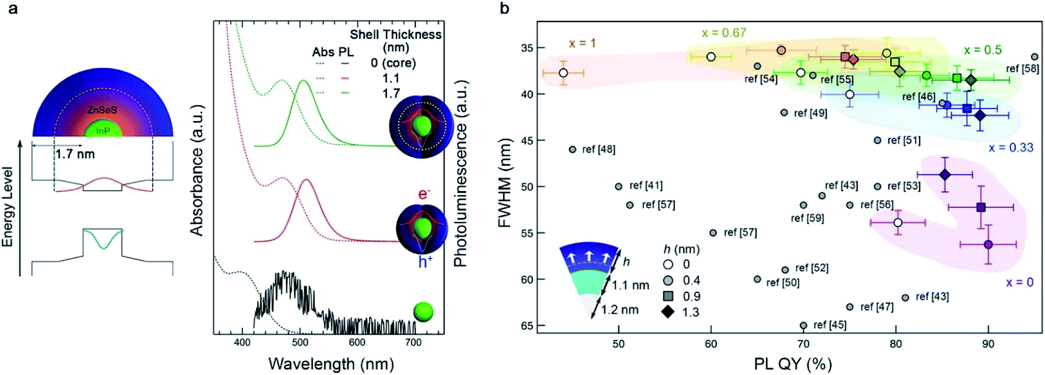 | ||
| Fig. 3 The core/shell approach for surface passivation. (a) Illustration of the InP/ZnSeS structure (left) and absorption and PL spectrum of InP and InP/ZnSeS (right), reproduced with permission from ref. 68. Copyright 2013 American Chemical Society (b) recently proposed design protocol for InP/ZnSeXS1−X/ZnS. Reproduced with permission from ref. 74. Copyright 2019 American Chemical Society. | ||
Even with the introduction of shells, III–V QDs still exhibit inferior optical properties compared to II–VI QDs. The charge imbalance that inherently exists at the interface between the III–V core and II–VI shell creates an internal trap state that is responsible for the PLQY loss of QDs. As evidenced from the success in II–VI monovalent core/shell QDs, we believe that the growth of III–V shell materials may greatly enhance the optical properties of III–V QDs. Further atomistic details on III–V QDs and their interfaces will provide a pathway to heterostructures that enable engineered exciton dynamics.
3.2 Etching of surface defects
In parallel with the core/shell heterostructuring, alternative chemical means that remove surface dangling bonds or oxidation layers have been explored (summarized in Table 2).8,41,75,76 The first attempt was performed by Olga I. Micic et al.,77 who observed strong band-edge emissions from InP QDs when exposed to dilute solutions of HF or NH4F. The fluoride chemicals eliminate (passivate) the surface deep states of InP QDs, reflected as the suppression of parasitic emission at lower energies with a long recombination lifetime (>500 ns). Later, D. V. Talapin et al. unveiled the surface etching of InP QDs with HF caused by the migration of photoexcited charge carriers to the P dangling bonds (Fig. 4a).75 Recently, milder etchants (e.g., 1-hexyl-3-methyl-imidazolium tetrafluoroborate (BF4)76) have been researched. The strategy that has been validated in InP QDs has also been applied to InAs QDs.78 Recently, S. Jeong et al. reported that nitrosyl tetrafluoroborate (NOBF4) is effective in removing not only the surface dangling bonds and native ligands, but also the amorphous oxides grown on InAs QDs (Fig. 4b and c).8| QD material | Etchants | Ligands | Etching condition | Result | Ref. |
|---|---|---|---|---|---|
| InP | HF, NH4F, N(C4H9)4F·3H2O, pyridine poly(hydrogen fluorine), HF-melamine complexes | TOPO or dodecanethiol | Photochemical etching with 450 W Xe lamp | PL QY 20–40% | 75 |
| KF, [18-crown-6] complex, hexadecylamine hydrofluoride | PL QY 3–5% | ||||
| InP | HF | TOPO with TOP | Photochemical etching with 450 W Xe lamp | PL QY 20–40% | 41 |
| InP | 1-Hexyl-3-methyl-imidazolium BF4, 1-butyl-4-methyl-pyridinium BF4 | Palmitate | Microwave synthesis | PL QY 1–47% | 76 |
| 1-Hexyl-3-methyl-imidazolium PF6 | PL QY 1–24% | ||||
| Tetrabutylammonium BF4 | PL QY 1–11% | ||||
| 1-Butyl-4-methyl-pyridinium PF6, tetrabutylammonium PF6, tetrabutylammonium fluoride, 1-hexyl-3-methyl-imidazolium Cl, 1-butyl-4-methyl-pyridinium Cl | PL QY below 3% | ||||
| InAs | Nitrosyl tetrafluoroborate (NOBF4) | Oleic acid | Chemical etching | Removal of oxide layer | 8 |
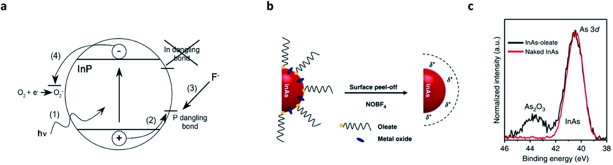 | ||
| Fig. 4 Surface etching on III–V QDs. (a) Suggested mechanism of HF treatment on InP QDs. The photogenerated hole activates P dangling states and the activated P site is removed by forming PF3. Oxygen scavenges electrons while holes are consumed at the P site. Reproduced with permission from ref. 41. Copyright 2005 American Institute of Physics. (b) Amorphous oxides, as well as the native ligands, on the surface of InAs QDs can be removed by NOBF4 etching. (c) 3d XPS patterns for InAs–oleate (black, before the etching) and naked InAs (red, after the etching) show successful removal of oxides. Reproduced with permission from ref. 8. Copyright 2018 Nature Publishing Group. | ||
Additionally, surface ligands can treat the traps for passivation after the synthesis. However, surface passivation using surface ligands after the synthesis is considered less effective in III–V nanocrystals when compared with II–VI or IV–VI nanocrystals because of the covalency in surface dangling bonds. Recently, the use of Z-type surface ligands for deep trap passivation has been demonstrated in InP nanocrystals with the PL efficiency increase of 10–50%.42,43 A more in-depth understanding of the surface is required for more precise passivation procedures. In the next section, we will discuss atomistic surface models of III–V QDs.
4. Atomistic understanding of the surface
4.1 Lessons learned from ionic QDs
For simplicity's sake, QDs are often considered to be spherical in shape with facet-independent surface characteristics. However, QDs are actually composed of various crystal facets that display different physical and chemical properties.19,79 Each crystal facet provides distinctive stoichiometry, and thus different chemical reactivities. Facet-specific surface chemistry of the ionic IV–VI QDs is well understood.19–23 For lead chalcogenide QDs, the crystal facets exposed on the surfaces consist of non-polar (100) and polar (111) facets. Atomistic surface understanding unveiled the origin of the size-dependent air-stability in lead chalcogenide QDs (Fig. 5a). Polar (111) facets exposing Pb atoms are fully passivated with oleate ligands, which results in complete passivation. By contrast, the stoichiometric (100) surfaces are self-passivated by Pb and chalcogenide (S, Se and Te) bonds without organic ligands, making them prone to oxidation.19 PbS QDs with a diameter below 4 nm that have surfaces terminated with only (111) facets are air-stable. However, PbS QDs with a diameter above 4 nm, on which the (100) facets emerge, are easily oxidized under air-exposure.19 In order to passivate the (100) facets, Woo et al. performed an in situ post-synthetic halide salt treatment on the PbSe QDs (Fig. 5b).20 This imparts size-independent air-stability and a higher PLQY, owing to the formation of a PbX2 (X = Cl, Br, I) adlayer on the (100) surface (Fig. 5c).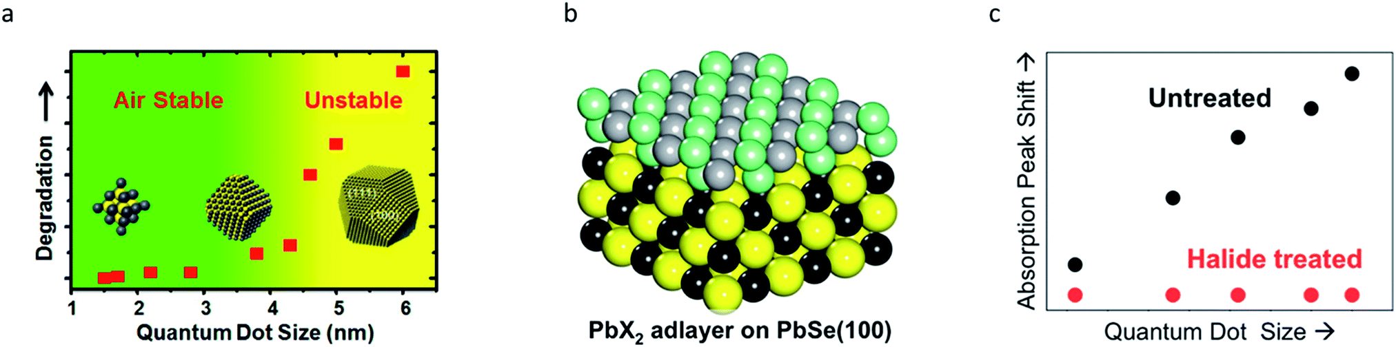 | ||
| Fig. 5 (a) Air stability of PbS QDs with respect to the diameter, exhibiting a stability transition at ∼4 nm due to their facet transition. Reproduced with permission from ref. 19. Copyright 2013 American Chemical Society. (b) Stochiometric (100) surface of PbSe QDs can be passivated by halides. (c) A significant increase in the stability of PbSe QDs after halide passivation is seen. Reproduced with permission from ref. 20. Copyright 2014 American Chemical Society. | ||
Based on facet change according to the particle size, it is possible to predict the facet of PbS QDs at a certain size and to design specific surface passivation or ligand exchange according to the predicted facet. The PbS QD atomistic surface model allows a better chemical treatment procedure for fabrication of PbS QD films with a desired energy level, carrier concentration, doping polarity, etc., leading to technological leaps in PbS QD solar cell research.3,80,81 Additionally, by leveraging the different surface energies of a specific facet, one can synthesize the extended structure of PbS nanosheets.82
Similarly, a deeper understanding of the III–V QD surface is expected to not only make significant improvements on surface passivation techniques, but also provide a method to tune energy levels with controlled surfaces or realizing extended structures.
4.2 Electron counting model with fractional dangling bonds in III–V QDs
It is particularly difficult to visualize the faceted surfaces of QDs with a very small size ranging around 1–10 nm. Therefore, the first-principles calculation or simulation can be a powerful tool to model the surface. To elucidate the surface of III–V QDs, Ko et al. investigated the coordination of the cation-rich surface and ligands of II–VI, IV–VI, and III–V QDs using the electron-counting model and DFT calculations.44 In the case of zinc blende InAs QDs with a tetrahedral bonding nature, the indium atoms in the QDs have three electrons and four bonds, which results in a fractional 0.75 electrons per bond. Accordingly, the As atoms in InAs QDs share five electrons with four bonds, and each As atom shares 1.25 electrons per bond. To passivate the InAs (100) surface, where indium has two dangling bonds with 1.5 electrons (Fig. 6a), two ligands donate three electrons to the dangling bonds. Thus, the surface becomes stable through co-passivation of one carboxylate or halide ligand, which can donate one electron, and one amine ligand, which can donate two electrons (Fig. 6c). Another method for stabilizing the InAs (100) surface involves passivating one monovalent anion ligand after In–In dimerization (Fig. 6b).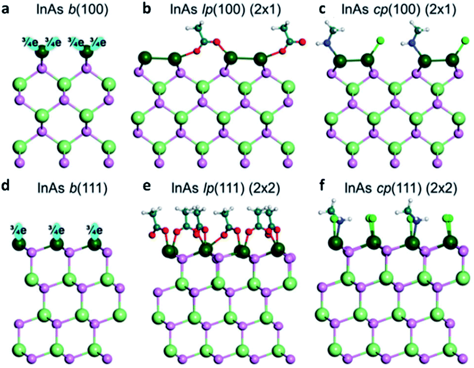 | ||
| Fig. 6 Atomistic view of the InAs QD (a–c) (100) surface and (d–f) (111) surface. b stands for the bare surface, lp for ligand passivation, and cp for co-passivation. Reproduced with permission from ref. 44. Copyright 2017 Royal Society of Chemistry. | ||
The InAs QD (111) surface has 0.75 electrons per dangling bond. Thus, a ligand with 1.25 electrons is required to stabilize the (111) surface of InAs QDs (Fig. 6d). However, there is no ligand that can provide 1.25 electrons under the colloidal QD synthesis conditions. To develop a method for passivating the InAs (111) surface, the (1 × 1) model is changed to a (2 × 2) model, such that four surface indium atoms have four dangling bonds with three electrons in the (2 × 2) model. To stabilize the (111) surface of InAs QDs in the (2 × 2) model, four ligands with five electrons are needed. To satisfy this requirement, the (111) surface of the InAs QDs must be passivated by three carboxylate or halide ligands, each of which can denote one electron, and one amine ligand, which can donate two electrons (Fig. 6f). These co-passivation methods are very important for stabilizing the surface of III–V QDs because it is more difficult to passivate the surface with only one type of ligand. Evidently, the stabilization energy is 53 meV Å−2 when passivated with only X-type ligands as shown in Fig. 6e, which is less than half the value (130 meV Å−2) of the co-passivation shown in Fig. 6f.44
4.3 Well-defined surface in III–V QDs
In spite of such desirable atomistic surface models, it is generally hard to analyze the surface-related characteristics of III–V QDs because of the ease of surface oxidation. Large oxophilicity of group III and V elements causes oxidation during and after the synthesis.59 The most commonly used fatty-acid ligands for III–V QD synthesis undergo ketonization reactions and produce H2O during the reaction at high temperature as follows:
H2O generated during the reaction oxidizes the III–V QD surfaces,61,83 so it is necessary to design a reaction that does not involve ketonization to understand the atomistic surface. Recent extensive investigation on InP clusters prepared at low temperature with defined atomic numbers and concrete view of the surfaces may help to understand the surface chemistry of InP nanocrystals and the surface energy driven synthetic pathways.84–87
Instead of fatty acid ligands, a new synthetic strategy uses indium halide with an amine-based V precursor (amino pnictide) as an alternative to (TMS)3P with In carboxylates, which is most commonly used in synthesis of InP QDs. The resulting InP QDs do not exhibit an oxidation signal in the P 2p spectrum in XPS analysis.88 This method not only avoids surface oxidation during the reaction but also is safer and less expensive than that using (TMS)3P with a fatty-acid.
More interestingly, in the synthesis using indium chloride (InCl3), aminophosphine in oleylamine can provide well-passivated fractional dangling bonds of the (111) facets of the zinc blende structure of III–V QDs. For example, one amine, which can give two electrons, and three chlorine that can give one electron can stabilize the (111) surface of InP, which requires 5 electrons in (2 × 2) surface indium atoms. As a result, tetrahedron shaped InP QDs with only the (111) facet can be synthesized (Fig. 7a).88 This was the first demonstration in which the shape of III–V QDs was precisely controlled in colloidal synthesis, with the exception of solution–liquid–solid methods that use the catalyst to control the growth direction.89,90 Subsequently, tetrahedron shaped InAs QDs were synthesized using InCl3, aminoarsine, and oleylamine by Talapin et al. (Fig. 7b).91
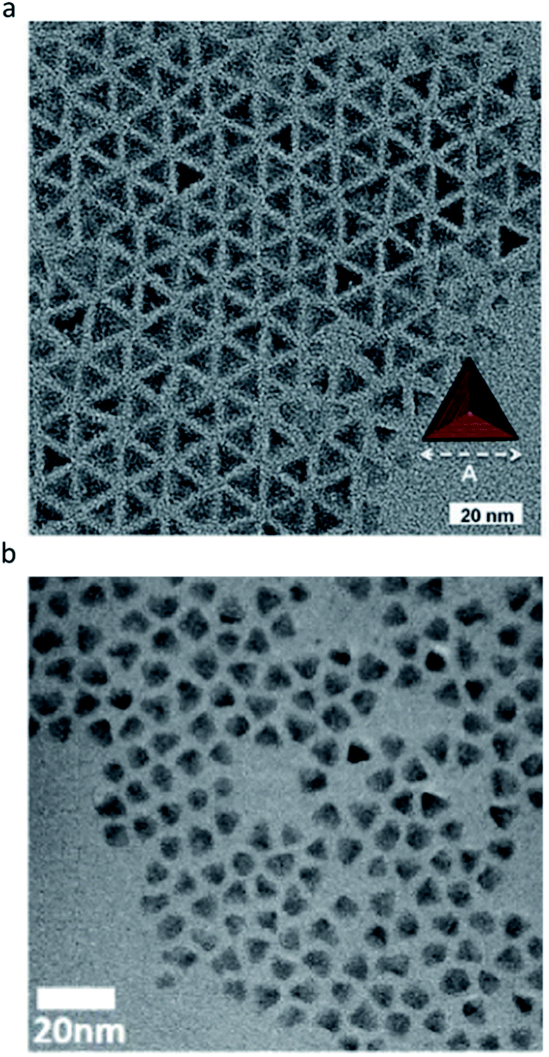 | ||
| Fig. 7 Tetrahedrally shaped III–V QDs. (a) InP QDs with the (111) facets exposed. Reproduced with permission from ref. 88. Copyright 2016 Wiley Online Library. (b) InAs QDs with the (111) facets exposed. Reproduced with permission from ref. 91. Copyright 2016 ACS Publications. | ||
Through these results, control of the surface energy based on the electron counting model effectively stabilizes the specific facets of III–V QDs. Furthermore, we expect that QDs with desired facets will be controlled by this method. Well-defined facets of QDs are highly desired tools for use in further research, such as facet specific surface–ligand interactions, reactivity, stability, and optoelectronic properties.
5. Summary and outlook
In this perspective, we discuss the problem of deep trap states expressed mainly by the covalent surfaces of III–V QDs. Deep traps in III–V QDs reduce the performance of the materials and severely limit their use in various applications. Therefore, eliminating surface defects is central to III–V QD research.Approaches for deep trap passivation of III–V QDs include removing deep traps via shelling, dangling bond etching, and post-synthetic ligand treatment. While success has been reported to an extent, to design a better chemistry for deep trap passivation, atomistic understanding on the surface structure is essential. Creating an un-oxidized surface in III–V QDs is the first step for adapting surface study protocols that have been developed extensively for ionic II–VI or IV–VI QDs. More importantly, formation of well-defined facets in III–V QDs will provide a simplified platform to investigate more detailed surface ligand interaction, atomistic interface structures, faceted surface energy driven growth, facet-specific stability, and many more, which are otherwise impossible to quantify because of the complex nature of covalent surfaces.
Conflicts of interest
There are no conflicts to declare.Acknowledgements
This research was supported by the Creative Materials Discovery Program through the National Research Foundation of Korea (NRF) funded by the Ministry of Science and ICT (MSIT) (2019M3D1A1078296), the NRF grant funded by the MSIT (2019R1A2B5B03070407 and 2018R1A2A2A14079326), and the grant (20173010013200) funded by KETEP and MOTIE and the Global Frontier R&D program of the Center for Multiscale Energy Systems (2017M3A6A7051087).References
- C.-F. Lai, Y.-C. Tien, H.-C. Tong, C.-Z. Zhong and Y.-C. Lee, RSC Adv., 2018, 8, 35966–35972 RSC.
- K.-H. Lee, C.-Y. Han, H.-D. Kang, H. Ko, C. Lee, J. Lee, N. Myoung, S.-Y. Yim and H. Yang, ACS Nano, 2015, 9, 10941–10949 CrossRef CAS PubMed.
- M. Yuan, M. Liu and E. H. Sargent, Nat. Energy, 2016, 1, 16016 CrossRef CAS.
- R. Debnath, O. Bakr and E. H. Sargent, Energy Environ. Sci., 2011, 4, 4870–4881 RSC.
- A. P. Litvin, I. V. Martynenko, F. Purcell-Milton, A. V. Baranov, A. V. Fedorov and Y. K. Gun'Ko, J. Mater. Chem. A, 2017, 5, 13252–13275 RSC.
- H. Choi, J. H. Song, J. Jang, X. D. Mai, S. Kim and S. Jeong, Nanoscale, 2015, 7, 17473–17481 RSC.
- J. H. Song and S. Jeong, Nano Convergence, 2017, 4, 21 CrossRef PubMed.
- J. H. Song, H. Choi, H. T. Pham and S. Jeong, Nat. Commun., 2018, 9, 4267 CrossRef PubMed.
- J. H. Song, X. D. Mai, S. Jeong and Y. H. Kim, J. Phys. Chem. Lett., 2017, 8, 5259–5263 CrossRef CAS PubMed.
- J. Li and J. J. Zhu, Analyst, 2013, 138, 2506–2515 RSC.
- G. Mandal, M. Darragh, Y. A. Wang and C. D. Heyes, Chem. Commun., 2013, 49, 624–626 RSC.
- I. V. Martynenko, A. P. Litvin, F. Purcell-Milton, A. V. Baranov, A. V. Fedorov and Y. K. Gun'Ko, J. Mater. Chem. B, 2017, 5, 6701–6727 RSC.
- X. Peng, Nano Res., 2009, 2, 425–447 CrossRef CAS.
- S. Tamang, C. Lincheneau, Y. Hermans, S. Jeong and P. Reiss, Chem. Mater., 2016, 28, 2491–2506 CrossRef CAS.
- M. C. Beard and R. J. Ellingson, Laser Photonics Rev., 2008, 2, 377–399 CrossRef CAS.
- R. D. Schaller, J. M. Pietryga and V. I. Klimov, Nano Lett., 2007, 7, 3469–3476 CrossRef CAS PubMed.
- A. Y. Chang, W. Liu, D. V. Talapin and R. D. Schaller, ACS Nano, 2014, 8, 8513–8519 CrossRef CAS PubMed.
- V. I. Klimov, Appl. Phys. Lett., 2006, 89, 87–90 CrossRef.
- H. Choi, J. H. Ko, Y. H. Kim and S. Jeong, J. Am. Chem. Soc., 2013, 135, 5278–5281 CrossRef CAS PubMed.
- J. Y. Woo, J. H. Ko, J. H. Song, K. Kim, H. Choi, Y. H. Kim, D. C. Lee and S. Jeong, J. Am. Chem. Soc., 2014, 136, 8883–8886 CrossRef CAS PubMed.
- J. Y. Woo, S. Lee, S. Lee, W. D. Kim, K. Lee, K. Kim, H. J. An, D. C. Lee and S. Jeong, J. Am. Chem. Soc., 2016, 138, 876–883 CrossRef CAS PubMed.
- A. J. Houtepen, Z. Hens, J. S. Owen and I. Infante, Chem. Mater., 2017, 29, 752–761 CrossRef CAS.
- C. Giansante and I. Infante, J. Phys. Chem. Lett., 2017, 8, 5209–5215 CrossRef CAS PubMed.
- L. E. Brus, J. Chem. Phys., 1984, 80, 4403 CrossRef CAS.
- P. R. Brown, D. Kim, R. R. Lunt, N. Zhao, M. G. Bawendi, J. C. Grossman and V. Bulović, ACS Nano, 2014, 8, 5863–5872 CrossRef CAS PubMed.
- D. M. Kroupa, M. Vörös, N. P. Brawand, B. W. McNichols, E. M. Miller, J. Gu, A. J. Nozik, A. Sellinger, G. Galli and M. C. Beard, Nat. Commun., 2017, 8, 15257 CrossRef CAS.
- K. A. Jackson and W. Schroter, Handbook of Semiconductor Technology: electronic structure and properties of semiconductors, WILEY-VCH, Verlag GmbH, D-69469 Weinheim (Federal Republic of Germany), 2000 Search PubMed.
- K. Seeger, Semiconductor Physics, Springer, Berlin, Heidelberg, 2004 Search PubMed.
- S. V. Gaponenko and H. V. Demir, Applied Nanophotonics, Cambridge University Press, 2018 Search PubMed.
- B. D. Pelatt, R. Ravichandran, J. F. Wager and D. A. Keszler, J. Am. Chem. Soc., 2011, 133, 16852–16860 CrossRef CAS.
- C. KIttel, Introduction to solid state physics, Hoboken, NJ, United States, 8th edn, 2005 Search PubMed.
- S. Z. Karazhanov, Semiconductors, 2005, 39, 161 CrossRef CAS.
- M. Hass and B. W. Henvis, J. Phys. Chem. Solids, 1962, 23, 1099–1104 CrossRef CAS.
- S. Tamang, S. Lee, H. Choi and S. Jeong, Chem. Mater., 2016, 28, 8119–8122 CrossRef CAS.
- S. Tamang, K. Kim, H. Choi, Y. Kim and S. Jeong, Dalton Trans., 2015, 44, 16923–16928 RSC.
- D. C. Gary, A. Petrone, X. Li and B. M. Cossairt, Chem. Commun., 2017, 53, 161–164 RSC.
- P. Ramasamy, K. J. Ko, J. W. Kang and J. S. Lee, Chem. Mater., 2018, 30, 3643–3647 CrossRef CAS.
- J. R. Heath, Chem. Soc. Rev., 1998, 27, 65 RSC.
- H. Fu and A. Zunger, Phys. Rev. B: Condens. Matter Mater. Phys., 1997, 56, 1496–1508 CrossRef CAS.
- P. Reiss, M. Protière and L. Li, Small, 2009, 5, 154–168 CrossRef CAS PubMed.
- S. Adam, D. V. Talapin, H. Borchert, A. Lobo, C. McGinley, A. R. B. de Castro, M. Haase, H. Weller and T. Möller, J. Chem. Phys., 2005, 123, 084706 CrossRef CAS PubMed.
- N. Kirkwood, J. O. V. V. Monchen, R. W. Crisp, G. Grimaldi, H. A. C. Bergstein, I. du Fossé, W. van der Stam, I. Infante and A. J. Houtepen, J. Am. Chem. Soc., 2018, 140, 15712–15723 CrossRef CAS PubMed.
- J. L. Stein, E. A. Mader and B. M. Cossairt, J. Phys. Chem. Lett., 2016, 7, 1315–1320 CrossRef CAS.
- J.-H. Ko, D. Yoo and Y.-H. Kim, Chem. Commun., 2017, 53, 388–391 RSC.
- P. Reiss, M. Carrière, C. Lincheneau, L. Vaure, S. Tamang, M. Carrière, C. Lincheneau, L. Vaure and S. Tamang, Chem. Rev., 2016, 116, 10731–10819 CrossRef CAS PubMed.
- S. Adachi, Properties of Semiconductor Alloys: Group-IV, III–V and II–VI Semiconductors, John Wiley & Sons, Ltd, Hoboken, NJ, United States, 2009 Search PubMed.
- P. Waltereit, O. Brandt, A. Trampert, H. T. Grahn, J. Menniger, M. Ramsteiner, M. Reiche and K. H. Ploog, Nature, 2000, 406, 865–868 CrossRef CAS PubMed.
- The National Renewable Energy Laboratory (NREL), Best Research-Cell Efficiency Chart, https://www.nrel.gov/pv/cell-efficiency.html, accessed, 11 July 2019 Search PubMed.
- A. C. Jones, Chem. Soc. Rev., 2004, 26, 101 RSC.
- D. C. Gary, B. a. Glassy and B. M. Cossairt, Chem. Mater., 2014, 26, 1734–1744 CrossRef CAS.
- D. Franke, D. K. Harris, L. Xie, K. F. Jensen and M. G. Bawendi, Angew. Chem., Int. Ed., 2015, 54, 14299–14303 CrossRef CAS PubMed.
- D. Hahm, D. Ko, B. G. G. Jeong, S. Jeong, J. Lim, W. K. K. Bae, C. Lee and K. Char, J. Inf. Disp., 2019, 20, 61–72 CrossRef CAS.
- J. Park, J. Joo, G. K. Soon, Y. Jang and T. Hyeon, Angew. Chem., Int. Ed., 2007, 46, 4630–4660 CrossRef CAS PubMed.
- S. G. Kwon and T. Hyeon, Small, 2011, 7, 2685–2702 CrossRef CAS.
- M. S. Daw and D. L. Smith, Phys. Rev. B: Condens. Matter Mater. Phys., 1979, 20, 5150–5156 CrossRef CAS.
- E. Cho, T. Kim, S. Choi, H. Jang, K. Min and E. Jang, ACS Appl. Nano Mater., 2018, 1, 7106–7114 CrossRef CAS.
- J. Jasieniak, M. Califano and S. E. Watkins, ACS Nano, 2011, 5, 5888–5902 CrossRef CAS PubMed.
- V. Srivastava, W. Liu, E. M. Janke, V. Kamysbayev, A. S. Filatov, C. J. Sun, B. Lee, T. Rajh, R. D. Schaller and D. V. Talapin, Nano Lett., 2017, 17, 2094–2101 CrossRef CAS PubMed.
- K. P. Kepp, Inorg. Chem., 2016, 55, 9461–9470 CrossRef CAS PubMed.
- M. D. Tessier, E. A. Baquero, D. Dupont, V. Grigel, E. Bladt, S. Bals, Y. Coppel, Z. Hens, C. Nayral and F. Delpech, Chem. Mater., 2018, 30, 6877–6883 CrossRef CAS.
- A. Cros-Gagneux, F. Delpech, C. Nayral, A. Cornejo, Y. Coppel and B. Chaudret, J. Am. Chem. Soc., 2010, 132, 18147–18157 CrossRef CAS PubMed.
- M. A. A. Hines and P. Guyot-Sionnest, J. Phys. Chem., 1996, 100, 468–471 CrossRef CAS.
- J. Lim, B. G. Jeong, M. Park, J. K. Kim, J. M. Pietryga, Y.-S. Park, V. I. Klimov, C. Lee, D. C. Lee and W. K. Bae, Adv. Mater., 2014, 26, 8034–8040 CrossRef CAS PubMed.
- J. Lim, Y.-S. Park, K. Wu, H. J. Yun and V. I. I. Klimov, Nano Lett., 2018, 18, 6645–6653 CrossRef CAS PubMed.
- J. Lim, Y.-S. Park and V. I. Klimov, Nat. Mater., 2018, 17, 42–49 CrossRef CAS PubMed.
- Y.-S. Park, J. Lim and V. I. Klimov, Nat. Mater., 2019, 18, 249–255 CrossRef CAS PubMed.
- W. K. Bae, L. A. Padilha, Y.-S. Park, H. McDaniel, I. Robel, J. M. Pietryga and V. I. I. Klimov, ACS Nano, 2013, 7, 3411–3419 CrossRef CAS PubMed.
- J. Lim, M. Park, W. K. Bae, D. Lee, S. Lee, C. Lee and K. Char, ACS Nano, 2013, 7, 9019–9026 CrossRef CAS PubMed.
- S. Kim, T. Kim, M. Kang, S. K. Kwak, T. W. Yoo, L. S. Park, I. Yang, S. Hwang, J. E. Lee, S. K. Kim and S.-W. Kim, J. Am. Chem. Soc., 2012, 134, 3804–3809 CrossRef CAS PubMed.
- S. Haubold, M. Haase, A. Kornowski and H. Weller, ChemPhysChem, 2001, 2, 331–334 CrossRef CAS PubMed.
- L. Li and P. Reiss, J. Am. Chem. Soc., 2008, 130, 11588–11589 CrossRef CAS PubMed.
- H. C. Wang, H. Zhang, H. Y. Chen, H. C. Yeh, M. R. Tseng, R. J. Chung, S. Chen and R. S. Liu, Small, 2017, 13, 1603962 CrossRef PubMed.
- J. Lim, W. K. Bae, D. Lee, M. K. Nam, J. Jung, C. Lee, K. Char and S. Lee, Chem. Mater., 2011, 4459–4463 CrossRef CAS.
- D. Hahm, J. H. Chang, B. G. Jeong, P. Park, J. Kim, S. Lee, J. Choi, W. D. Kim, S. Rhee, J. Lim, D. C. Lee, C. Lee, K. Char and W. K. Bae, Chem. Mater., 2019, 31, 3476–3484 CrossRef CAS.
- D. V. Talapin, N. Gaponik, H. Borchert, A. L. Rogach, M. Haase and H. Weller, J. Phys. Chem. B, 2002, 106, 12659–12663 CrossRef CAS.
- D. D. Lovingood and G. F. Strouse, Nano Lett., 2008, 8, 3394–3397 CrossRef CAS.
- O. I. Micic, J. Sprague, Z. Lu and A. J. Nozik, Appl. Phys., 1996, 68, 3150–3152 CAS.
- T. G. Kim, D. Zherebetskyy, Y. Bekenstein, M. H. Oh, L. W. Wang, E. Jang and A. P. Alivisatos, ACS Nano, 2018, 12, 11529–11540 CrossRef CAS PubMed.
- M. A. Boles, D. Ling, T. Hyeon and D. V. Talapin, Nat. Mater., 2016, 15, 141–154 CrossRef CAS PubMed.
- J. H. Song, H. Choi, Y.-H. H. Kim and S. Jeong, Adv. Energy Mater., 2017, 7, 1–6 Search PubMed.
- G. H. Carey, A. L. Abdelhady, Z. Ning, S. M. Thon, O. M. Bakr and E. H. Sargent, Chem. Rev., 2015, 115, 12732–12763 CrossRef CAS.
- C. Schliehe, B. H. Juarez, M. Pelletier, S. Jander, D. Greshnykh, M. Nagel, A. Meyer, S. Foerster, A. Kornowski, C. Klinke and H. Weller, Science., 2010, 329, 550–553 CrossRef CAS PubMed.
- L. Xie, D. K. Harris, M. G. Bawendi and K. F. Jensen, Chem. Mater., 2015, 27, 5058–5063 CrossRef CAS.
- D. C. Gary, M. W. Terban, S. J. L. Billinge and B. M. Cossairt, Chem. Mater., 2015, 27, 1432–1441 CrossRef CAS.
- D. C. Gary, S. E. Flowers, W. Kaminsky, A. Petrone, X. Li and B. M. Cossairt, J. Am. Chem. Soc., 2016, 138, 1510–1513 CrossRef CAS PubMed.
- Q. Zhao and H. J. Kulik, Chem. Mater., 2018, 30, 7154–7165 CrossRef CAS.
- A. Ritchhart and B. M. Cossairt, Inorg. Chem., 2019, 58, 2840–2847 CrossRef CAS PubMed.
- K. Kim, D. Yoo, H. Choi, S. Tamang, J. Ko, S. Kim, Y. Kim and S. Jeong, Angew. Chem., 2016, 55, 1–6 CrossRef.
- F. Wang, A. Dong and W. E. Buhro, Chem. Rev., 2016, 116, 10888–10933 CrossRef CAS PubMed.
- S. Kan, A. Aharoni, T. Mokari and U. Banin, Faraday Discuss., 2004, 125, 23–38 RSC.
- V. Srivastava, E. M. Janke, B. T. Diroll, R. D. Schaller and D. V. Talapin, Chem. Mater., 2016, 28, 6797–6802 CrossRef CAS.
Footnote |
| † These authors contributed equally to this work. |
| This journal is © The Royal Society of Chemistry 2020 |