
 Open Access Article
 This Open Access Article is licensed under a Creative Commons Attribution-Non Commercial 3.0 Unported Licence
Effects of Cr- and Mn-alloying on the band gap tuning, and optical and electronic properties of lead-free CsSnBr3 perovskites for optoelectronic applications
Md Ibrahim Kholil * and
Md Tofajjol Hossen Bhuiyan*
* and
Md Tofajjol Hossen Bhuiyan*
Department of Physics, Pabna University of Science and Technology, Pabna-6600, Bangladesh. E-mail: ibrahim.physics20@gmail.com; thbapon@gmail.com; thbapon@pust.ac.bd
First published on 9th December 2020
Abstract
Nowadays, lead-free metal halide perovskite materials have become more popular in the field of commercialization owing to their potential use in solar cells and for other optoelectronic applications. In this study, we used density functional theory to determine the different optoelectronic properties, such as structural, optical, electronic, and elastic properties, of pure CsSnBr3 and metal (Cr/Mn) alloyed CsSnBr3. The present study suggests high absorption with a narrow band gap, a high dielectric effect, high conductivity, and reasonable reflectivity in the visible region under metal alloying. The calculated absorption coefficients indicate that the absorption edge mainly shifted (red-shift) towards the lower energy region in the event of alloying, and a clear peak was observed in the visible region. The creation of an intermediate state (dopant level) in the band structure of the alloying samples allows excited photoelectrons to transfer from the valence band to the conduction band. The alloying materials exhibit a highly ductile nature and are mechanically stable as pristine samples. The alloying effects seen in the present investigation suggest that Mn-alloyed CsSnBr3 is remarkable, showing appropriate characteristics for use in solar cell devices and for other optoelectronic applications in comparison with other lead-free (toxin-free) perovskite materials.
1. Introduction
Metal halide perovskite series semiconductor type materials have recently gained significant interest in the scientific community owing to their high performance in solar cell applications and their extraordinary optoelectronic properties, including their high absorption of visible light with a narrow band gap, excellent mobility of the charge carrier, high dielectric value, high conductivity, reduced reflectivity, reduced charge carrier recombination rate, and low excitation binding energy.1,2 This family of semiconductors with the chemical formula ABX3 (in which A represents the positive ion, B reveals the metal ion, and X is a halogen anion) are also used in electronic devices, such as photodetectors, light-emitting diodes (LEDs), and solar-to-fuel energy conversion devices owing to their unique optoelectronic features.3–6 Moreover, nowadays, metal halide semiconducting materials are more efficient and profitable to use in photovoltaic applications compared to silicon-based technology.1 In particular, the perovskite materials are affordable and numerously available on earth. Therefore, research into these materials has shown rapid progress in the scientific community, as well as having potential uses in photovoltaic applications.Among the perovskites materials that have attracted significant interest owing to their excellent power-conversion efficiencies in device applications, the majority are lead halide perovskites. Although these materials reveal potential features for photovoltaic applications, these materials are not suitable owing to their anti-environmental nature. Consequently, lead halide perovskite materials are not friendly in nature owing to the presence of toxic Pb, and hence significant concerns naturally arise about their practical uses in device applications. For instance, the combination of PbI2 as a Pb-based perovskite material is noxious under environmental conditions.7–9 On the other hand, lead-based perovskites show some drawbacks in device applications such as device instability and J–V hysteresis.10 Therefore, researchers have aimed to replace the Pb contained in perovskites with a suitable metal cation. As a consequence, several theoretical and experimental investigations have been published in the literature in recent years concerning the replacement of Pb.11–13
The optical properties of the Pb free perovskite material CsSnBr3 reported by Roknuzzaman et al.11 reveal a medium absorption and reduced conductivity in the visible region. Consequently, CsSnBr3 is not suitable for practical uses in solar cells and other optoelectronic applications. Although this material is ductile in nature, it shows a large experimental band gap value of 1.75 eV.14 The wider band gap is also another reason for failure in device applications. A suitable metal alloy can reduce the wider band gap by creating a dopant level and significantly enhance the absorption in the visible region, as well as the conductivity. Therefore, in this study, we have created a plan to alloy a specific metal in the Sn position of CsSnBr3 that reduces the wider band gap and, hence, potentially improves the absorption of the whole region in the solar spectrum.
Coduri et al. recently experimentally studied the metal halide perovskite CsSnBr3 in order to tune the structural and optical properties for potential use in photovoltaic (PV) applications.15 In 2018, Mahmood et al.16 theoretically predicted the mechanical, optoelectronic and thermoelectric properties of CsSnBr3 for solar cells, optoelectronic, and thermoelectric devices, but the calculated band gap is relatively large compared to the experimental band gap (1.75). In 2011, Brik17 calculated the electronic, optical, and elastic properties by using density functional theory (DFT) and suggested that the material possesses a very small band gap. Although the material shows a narrow band gap, the calculated value of the Poisson's ratio is 0.0809, which reveals that it is brittle in nature. Another perovskite material CsGeI3 studied by Roknuzzaman et al.11 suggested that it was the best inorganic metal halide perovskite, but their study revealed the brittle nature of CsGeI3. On the other hand, their study revealed that the conductivity of CsGeBr3 and CsGeCl3 perovskites are not desirable compared to the CsGeI3 perovskite, but these are good compared to the lead halide perovskites. As a consequence of the lack of perovskites to use in optoelectronic applications, several doping effect calculations have been carried out to tune the band gap and enhance the optoelectronic properties.12,18,19 It has been previously reported that the metal-doped CsGeCl3 has a Poisson's ratio that lies in a critical position. Therefore, CsGeCl3 is not considered highly ductile in nature.18 On the other hand, CsSnCl3, using metal doping, was reported in the literature and a high absorption and high conductivity were predicted, but the metal-doped samples revealed a high reflectivity. In contrast, metal-doped CsGeBr3 predicted by Islam et al.12 suggested an enhanced band gap nature, but the material reveals a medium absorption and reduced conductivity in the visible region. The symmetry of a supercell is essential to finding the appropriate characteristic, which is not found in the metal-doping band structures available in the literature.18,19 On the other hand, we used supercell symmetry (as shown in the high symmetry points in Fig. 5) that represent our calculation compared to others. Therefore, in the present study, we aim to investigate the metal (Cr/Mn) alloying effect in CsSnBr3 to determine the narrow band nature, as well as the optimum absorption and conductivity nature with reduced reflectivity in the visible region by using DFT. Furthermore, we also examined the nature of the ductility along with other elastic properties. Finally, we aim to create a comparison of significant features among the lead-free perovskite materials with our metal-alloyed CsSnBr3 samples.
2. Computational methods
The DFT20,21 based computation investigations were performed by using the Cambridge Serial Total Energy Package (CASTEP) code22 with the aid of the plane-wave pseudopotential. The ultrasoft pseudopotential is used here as a Vanderbilt type for the description of electron–ion interactions.23 The geometry optimization was performed using the generalized gradient approximation (GGA) within the Perdew–Burke–Ernzerhof (PBE) functional for exchange–correlation interactions.24 For the geometry optimization calculations, the plane wave cutoff energy was set to 600 and 350 eV for the pristine sample CsSnBr3 and the metal (Cr/Mn) alloyed CsSnBr3. A high symmetry points (k-points) mesh was used of 14 × 14 × 14 and 3 × 3 × 3 for the pure form of CsSnBr3 and alloyed form of CsSnBr3 to ensure better convergence.25 The ground state position of the crystal structure was confirmed by minimizing the total energy, internal forces, and external stresses, as well as using BFGS (Broyden–Fletcher–Goldfarb–Shanno) techniques.26 The single elastic constant was calculated by using the finite strain theory27 and the theory employed set homogeneous strains, which were performed on the unit cell to relax the atomic degree of freedom.12 In the set of the homogeneous strain, there are six-stress components σij that work in a unit cell under each strain δj. A scissor value of 1.196 was employed during optical properties analysis to diminish the band gap within the theoretical (0.5539 eV) and experimental (1.75 eV) one. The formula that was used to calculate the present optical properties is available in the literature.283. Results and discussion
3.1. Structural properties
The lead-free (non-toxic) metal halide CsSnBr3 perovskite crystallizes in a cubic structure with the space group Pm![[3 with combining macron]](https://www.rsc.org/images/entities/char_0033_0304.gif) m (no. 221) and the unit cell consists of five atoms (one Cs atom, three Br atoms, and one Sn atom). The fractional coordinates of these atoms are (0, 0, 0) for Cs with a 1a Wyckoff site, (0.5, 0.5, 0.5) for Sn with a 1b Wyckoff site and (0, 0.5, 0.5) for Br with a 3c Wyckoff site, respectively.11 Here, we constructed a 2 × 2 × 2 supercell of the cubic unit cell for alloying (Fig. 1). Therefore, the unit cell increases eight times in the supercell, as well as an eight-fold increase in the number of atoms. Generally, in the supercell 8 Sn atoms are found (one in the unit cell) and one of these atoms is replaced by a Cr/Mn atom (substitutional alloying). Herein, the substitutional alloying is considered to be 12.5% and hence the following formula is found, CsSn0.875Cr0.125Br3 or CsSn0.875Mn0.125Br3. The optimized structural parameter results for the pure cell and alloying cells are tabulated in Table 1. The calculated equilibrium structural parameters a and V are in good agreement with the available experimental and theoretical results. It is perceived that the structural parameters are reduced owing to metal alloying. The observed change in the lattice parameter and unit cell volume of the alloyed samples occurred as a result of the smaller value of the ionic radii of the (Cr/Mn) dopant elements [Cr2+ (0.73 Å)/Mn2+ (0.67 Å)] compared to the Sn atom [Sn2+ (1.10 Å)].10,29
m (no. 221) and the unit cell consists of five atoms (one Cs atom, three Br atoms, and one Sn atom). The fractional coordinates of these atoms are (0, 0, 0) for Cs with a 1a Wyckoff site, (0.5, 0.5, 0.5) for Sn with a 1b Wyckoff site and (0, 0.5, 0.5) for Br with a 3c Wyckoff site, respectively.11 Here, we constructed a 2 × 2 × 2 supercell of the cubic unit cell for alloying (Fig. 1). Therefore, the unit cell increases eight times in the supercell, as well as an eight-fold increase in the number of atoms. Generally, in the supercell 8 Sn atoms are found (one in the unit cell) and one of these atoms is replaced by a Cr/Mn atom (substitutional alloying). Herein, the substitutional alloying is considered to be 12.5% and hence the following formula is found, CsSn0.875Cr0.125Br3 or CsSn0.875Mn0.125Br3. The optimized structural parameter results for the pure cell and alloying cells are tabulated in Table 1. The calculated equilibrium structural parameters a and V are in good agreement with the available experimental and theoretical results. It is perceived that the structural parameters are reduced owing to metal alloying. The observed change in the lattice parameter and unit cell volume of the alloyed samples occurred as a result of the smaller value of the ionic radii of the (Cr/Mn) dopant elements [Cr2+ (0.73 Å)/Mn2+ (0.67 Å)] compared to the Sn atom [Sn2+ (1.10 Å)].10,29
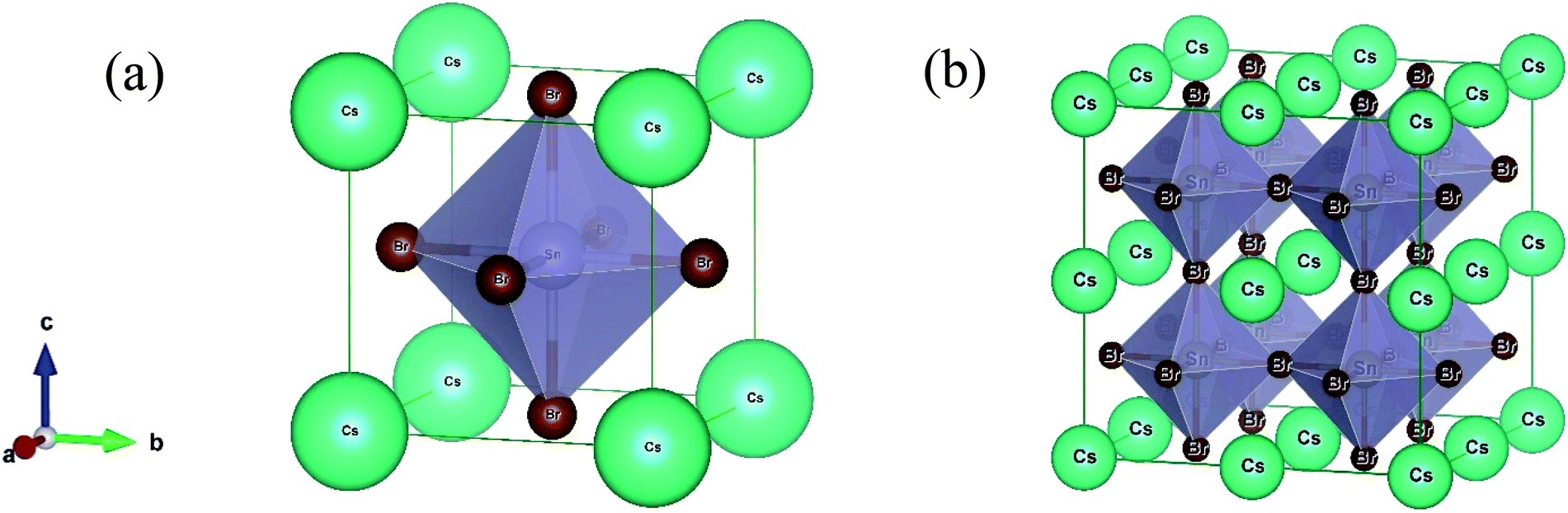 | ||
| Fig. 1 The crystal structure of CsSnBr3: (a) unit cell and (b) constructed (2 × 2 × 2) supercell. | ||
3.2. Optical properties
Studying the optical properties of material provides essential information about the light energy interactions with substances. The optical behavior is crucial to understanding the inner electronic configuration of a substance, and thereafter the efficient uses in the field of photovoltaic applications, such as solar cells. The lead-free (non-toxic) pure material CsSnBr3 reveals a medium quality absorption and reduced optical photoconductivity, and hence the pure form of the material is not more desirable for use in solar cell technology.11 Accordingly, we performed a detailed calculation of the different optical functions, such as the absorption spectra, reflectivity, photoconductivity, and dielectric function of the intrinsic and transition metal alloyed (Cr and Mn) non-toxic CsSnBr3 perovskite to determine the optimum properties for solar cell devices, as well as other optoelectronic applications.The calculated absorption spectra of pure CsSnBr3 and alloyed CsSnBr3 perovskites are shown in Fig. 2. The absorptivity nature of material defines how much energy is absorbed when light energy penetrates the substance. During the penetration, the penetration of the light energy decreases until it is fully absorbed by the materials. The nature of absorption can be determined by the quality of the absorption coefficient, as shown in Fig. 2. The absorption coefficient provides an idea of the capability of a substance to achieve the highest solar energy conversation, and hence whether it is a suitable high performance material for use in solar cell devices. The absorption spectra are presented in Fig. 2a as the photon energy. Fig. 2a proves that the alloyed absorption spectra is significantly shifted towards the lower energy region (red-shift). Both the Mn- and Cr-alloyed spectra reveal high absorption in the visible energy region. The addition peak has also been observed for the Mn- and Cr-alloyed absorption spectra. The Mn-alloyed CsSnBr3 reveals the greater absorption coefficient compared to that of Cr-alloyed CsSnBr3. The clear reason for this separation between the two-alloyed samples is revealed in the section on electronic properties. On the other hand, the absorption coefficient of the pure form of CsSnBr3 revealed that there are no high peaks in the visible energy region compared to the alloyed samples. The enhanced absorption coefficient of CsSnBr3 is achieved in the visible region owing to the metal alloying effect.
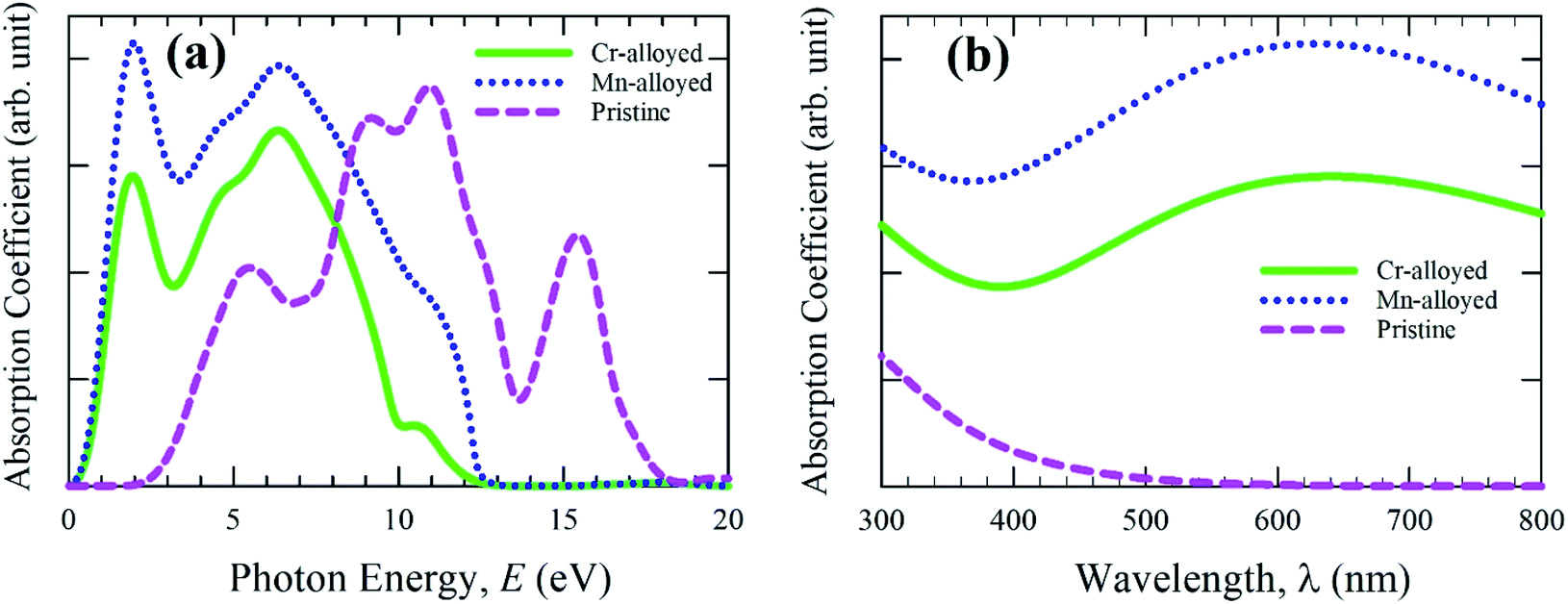 | ||
| Fig. 2 Absorption spectra of pristine and metal-alloyed CsSnBr3 as a function of (a) light energy and (b) the wavelength of light. | ||
The absorption coefficient as a function of the wavelength of light was also investigated to ensure the light absorption phenomena in the visible region and the results are presented in Fig. 2b. The observed results of the absorption coefficient as a function of the wavelength are higher for both the alloyed samples compared to the pristine sample. A significant change has also been noted from Fig. 2b between the pure and alloyed materials owing to the metal-alloyed effects in the whole region. Semiconducting materials with a wider band gap are capable of capturing 4% of the ultraviolet (UV) light of the solar energy that arrives on Earth.31 On the other hand, the materials are capable of capturing visible light that makes up about 43% of the solar energy spectrum.32 Consequently, the pure form of the CsSnBr3 perovskite with a wider band gap (1.75 eV) does not have the ability to properly utilize the visible light energy of the solar spectrum and hence is not preferable to use in the solar cell. The visible light absorption of the Mn-alloyed CsSnBr3 showed more absorption compared to the Cr-alloyed. Considering the absorption nature, it is concluded that the Mn-alloyed sample could be an appropriate candidate for utilization of the solar energy spectrum and hence its performance might be suitable for use in solar cells.
The calculated optical conductivity (real part) or photoconductivity spectra is shown in Fig. 3a, which is responsible for the electrical conductivity and hence increases owing to the absorption of incident light energy. The optical conductivity is calculated for up to 12 eV of photon energy. The conductivity of Cr- and Mn-alloyed CsSnBr3 is approximately equal above the photon energy 4.0 eV. A very sharp peak is observed in the low energy region for both metal-alloyed cases. The conductivity of the Mn-alloyed is higher compared to the Cr-alloyed, as shown clearly in the low energy region. In the low energy region, the highest conductivity is observed owing to the higher absorption that occurs in the visible region (Fig. 2).
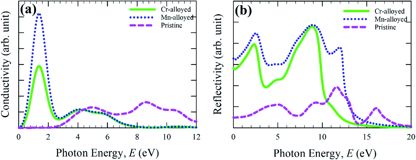 | ||
| Fig. 3 Calculated optical spectra: (a) conductivity and (b) reflectivity of pure and (Cr/Mn)-alloyed CsSnBr3 perovskite. | ||
The reflectivity of a material measures the ability of a material to reflect the incident light energy of the material surface and hence this phenomenon is crucial for determining a suitable substance for photovoltaic applications. The optical function, reflectivity, is calculated for up to 20 eV photon energy, and the calculated reflectivity spectra are shown in Fig. 3b for both pure and alloyed samples. The calculated reflectivity spectra show that a low reflectivity is exhibited over the energy region for a pristine sample, whereas the alloyed sample exhibited a higher reflectivity. However, the reflectivity of the metal-doped CsSnBr3 was comparatively small in comparison to CsSnCl3 and CsGeCl3.18,19 Peaks are also observed for the alloyed materials in the UV region and the reflectivity becomes zero at around 17 eV. From Fig. 3b, it can be seen that the reflectivity of the Mn-alloyed material is higher compared to the Cr-alloyed material. Consequently, the high reflectivity of the alloyed sample is not suitable for solar cell applications. In that case, further investigation should be performed to reduce the higher reflectivity in the visible region of the metal-alloyed CsSnBr3 perovskites, which may significantly enhance the absorption and, hence, may increase the performance of the solar cells.
The real and imaginary parts of the dielectric function (Fig. 4a) are calculated up to a photon energy of 12 eV. Studying the dielectric function is essential to understanding the information about the charge-recombination rate, as well as the efficiency of optoelectronic devices.33 The high static value of the dielectric function is important to reducing the high charge-recombination rate to a low charge-recombination and hence significantly improves the performance of optoelectronic devices. The studied real part and imaginary part clearly represent the remarkable dielectric value of the alloyed material, whereas the pure form of CsSnBr3 has a negligible effect compared to the alloyed material. In comparison, the wider band gap material shows a low dielectric value.34 In addition, the band gap increases, whereas the value of the dielectric constant decreases.35 As a result, the free carriers decrease during the increasing band gap and hence there is a decrease in the value of the dielectric constant. Therefore, the studied metal-alloyed material shows a high dielectric value owing to the lower band gap compared to the pristine material, which is clearly shown in the electronic band structure. The imaginary part of the dielectric function (Fig. 4b) is responsible for a clear representation of the electronic band structure and the optical function, such as the absorptive behavior of a material.36 The sharp peaks of the imaginary part of dielectric functions in the visible region indicate that high absorption occurs in the visible region, which is clearly shown in the absorption spectra (Fig. 2). The Cr-alloyed and Mn-alloyed material both have a high dielectric constant value, but the Mn-alloyed material is comparatively high, and hence the Mn-alloyed material is expected to be a promising candidate for optoelectronic applications. The studied metal-alloyed sample becomes transparent in the high-energy region (above 7 eV) owing to the negligible dielectric effect.
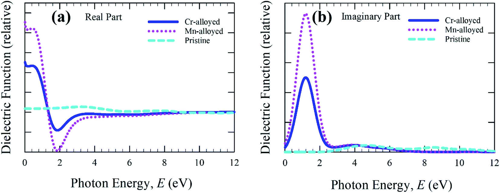 | ||
| Fig. 4 The (a) real part and (b) imaginary part of dielectric function as a function of the photon energy of the pristine and alloyed materials. | ||
3.3. Electronic properties
To elucidate the optical function of CsSnBr3, here, we calculated the electronic band structure represented in Fig. 5. Generally, we know from the semi-conductive theory, the band close to the Fermi level is significant for revealing the physical performance of a material. The semi-conductive theory further states that the valence band (VB) maximum and conduction band (CB) minimum represent the band gap. Therefore, we mainly focus on the VB and CB close to the Fermi level to signify the performance. Fig. 5a represents the band structure of pure CsSnBr3. The maximum of the VB and the minimum of the CB reveals a R high symmetry point that indicates the direct band gap material. The calculated band gap is 0.614 eV. This band gap value of pure CsSnBr3 is well-matched with the band gap values published by Roknuzzaman et al.11 and Körbel et al.,37 which indicates the reliability of the present work. The calculated band structure of the pure supercell (eight times) (Fig. 5b) also reveals the direct band gap semiconductor with the band gap (Eg = 0.5539 eV) at the R k-points. The pure supercell results are consistent with those of the pure unit cell. The observed band gap results of the pure single-cell and pure supercell represent the large difference with an experimental band gap value, 1.75 eV,14 which occurs due to the GGA process. Underestimation is usually a significant limitation of the GGA process and this emerged mainly because of the correlation effects and electron–electron exchange approximation. Using hybrid functions38 and the GW method39 instead of GGA, can help overcome the underestimation but still, there are some limitations. On the other hand, the GGA+U method partially fixed the underestimation.40 However, we mainly focus on the comparative analysis of the pure form and alloy form of CsSnBr3, and the GGA approach does not influence the comparison.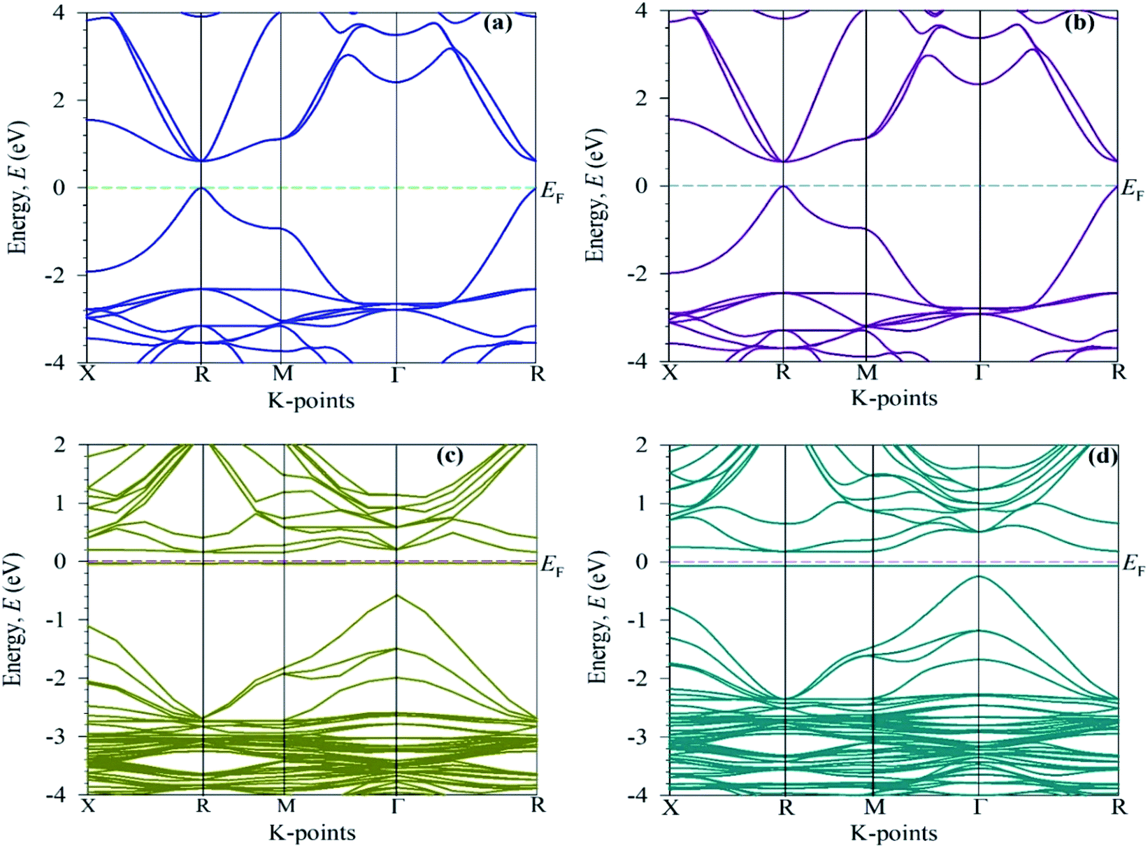 | ||
| Fig. 5 Electronic band structures: (a) the pure unit cell, (b) the 2 × 2 × 2 supercell, and (c) the Cr-alloyed and (d) the Mn-alloyed CsSnBr3 perovskite. | ||
The electronic band structure of the Cr-alloyed supercell (Fig. 5c) indicates that the VB maximum occurs at gamma (Γ) points and the CB minimum occurs at R points. As we know, the two different points of the VB maximum and CB minimum denote the indirect band gap of the material. Therefore, the indirect band gap of Cr-alloyed materials (Eg = 0.726 eV) semiconductor was considered. However, an intermediate state is observed between the VB and CB. The intermediate state acts at the electron donor level and the donor level contains an additional valence electron. The valence electron in the intermediate state holds energy close to the conduction band. The band gap between the intermediate state and CB minimum is 0.178 eV, which is much smaller compared to the pure form of CsSnBr3. Owing to the intermediate state, the valence electron close to the CB can be easily excited by gaining visible light energy and spontaneously leaps from the VB to CB and hence increases the absorptive nature of a material. Consequently, a significant absorptive nature (Fig. 2) of the Cr-alloyed material has been found compared to the pure form. The calculated band structure of the Mn-alloyed CsSnBr3, represented in Fig. 5d, reveals that the VB maximum occurs at gamma (Γ) points and the CB minimum occurs at R points. Therefore, the material is considered an indirect band gap material (Eg = 0.422 eV). Here, a band gap of 0.241 eV was evaluated between the intermediate state and CB minimum. The observed band gaps of the pure and metal-alloyed samples are tabulated in Table 2. The studied results of the pure and alloyed forms indicate that the Mn-alloyed materials have a lower band gap by comparison with the pure and Cr-alloyed samples. Consequently, in the Mn-alloyed material, a large number of electrons were transferred from the VB to the CB, and hence the absorption significantly increased (Fig. 2) compared to the Cr-alloyed and pristine materials. The higher results of the absorption coefficient of the Mn-alloyed material suggest that it is a more promising candidate for solar cell devices in comparison to the pristine and Cr-alloyed form. The observed band gap of the pristine CsSnBr3 and metal (Cr/Mn) alloyed CsSnBr3 samples are represented in Fig. 6a and b schematic diagram (Fig. 6a) is included to clarify the energy band and band gap.
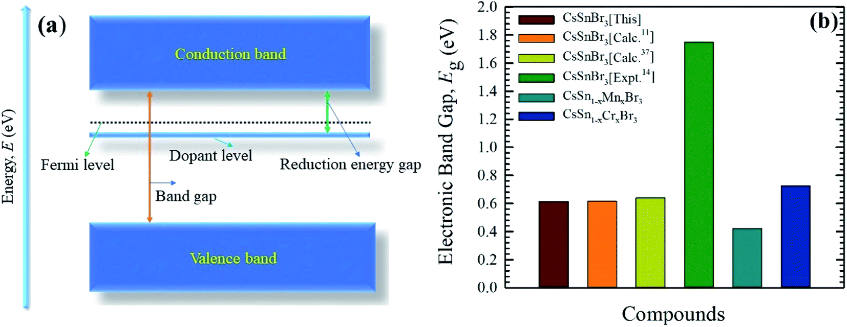 | ||
| Fig. 6 A schematic diagram of the energy band (a), and the observed band gaps (b) of pure and metal-alloyed CsSnBr3. | ||
The calculated total density states (TDOSs) and partial density of states (PDOSs) are shown in Fig. 7. The vertical dotted line between the VB and CB indicates the Fermi level. The TDOSs of the VB (lower energy portion) of a pure supercell (Fig. 7a) mainly arise owing to the contribution of the Sn-5p and Br-4p states with a little admixture of the Cs-6s, Cs-5p, and Sn-5p states. On the other hand, the upper energy portion (CB) consists of the Cs-5p and Br-4s states with some admixture of Cs-6s, Sn-5p, Sn-5s, and Br-4p.
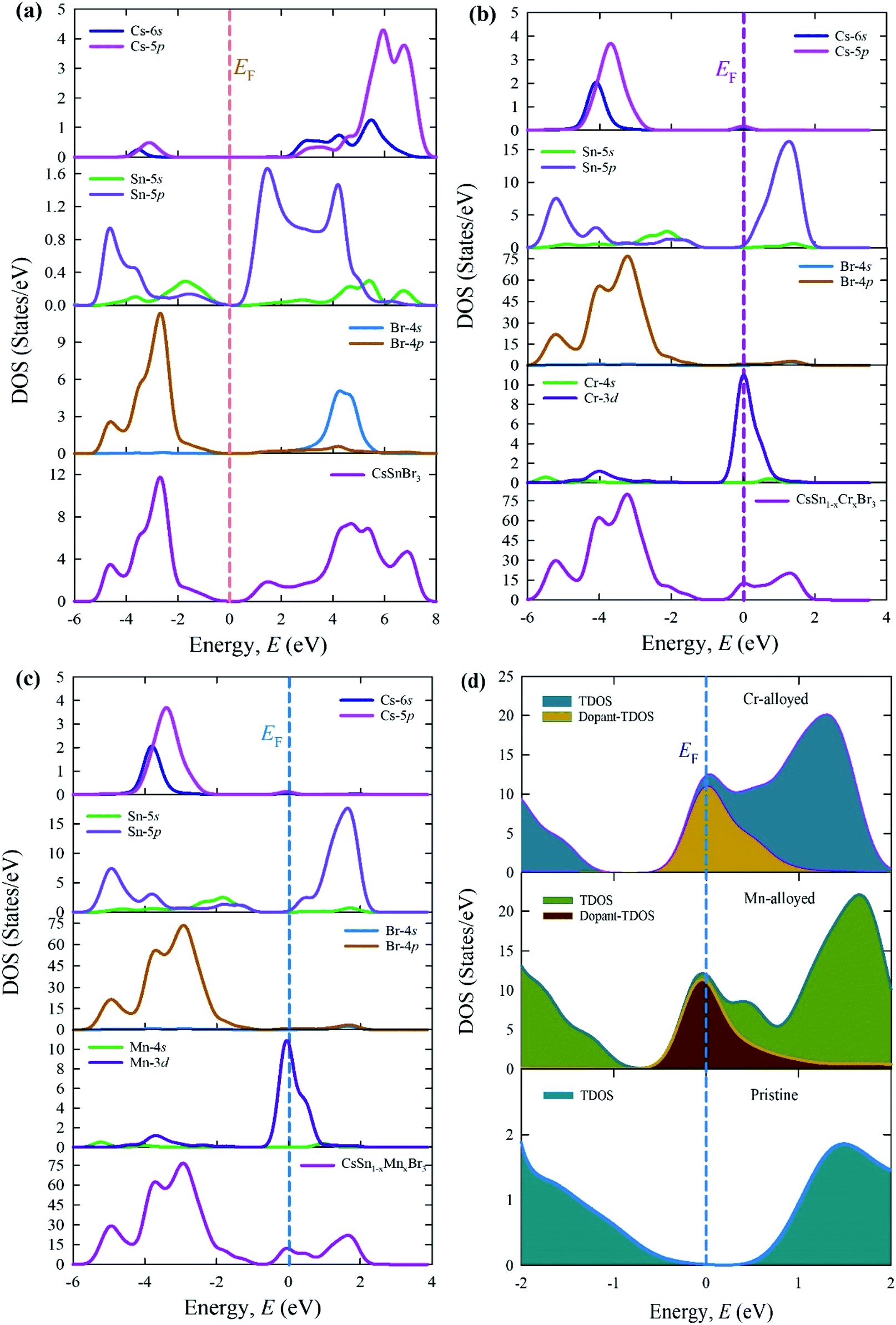 | ||
| Fig. 7 Total and PDOSs of (a) the pure supercell and (b) Cr-alloyed and (c) Mn-alloyed perovskites, and (d) the dopant contributions close to the Fermi levels of CsSnBr3 perovskites. | ||
Fig. 7b and c illustrate the TDOSs and PDOSs of the Cr-alloyed and Mn-alloyed CsSnBr3. The observed results of the alloyed samples indicate that the density of states (DOSs) contribution in conduction mainly arises from the Sn-5p states. A similar contribution appears for both alloyed materials. An important observation between the pure and alloyed samples is that the Fermi level is shifted towards the conduction and this occurred due to the alloying effect. The creation of the extra peaks that are observed in the dopant DOSs, are mainly a result of the Cr-3d states for the Cr-alloyed and the Mn-3d states for the Mn-alloyed samples of CsSnBr3.
Fig. 7d elucidates the dopant contribution close to the Fermi level that contributes to the change in the band gap energy and hence a dopant energy state that is exhibited inside the band gap, called the intermediate state. The intermediate states are mainly responsible for the transfer of the valence electron to the CB. In this case, the excited electron, under visible light absorption, first moves to the dopant energy states and finally goes onto the CB. These results are the prime cause for the shift of the Fermi level towards the CB, in addition to the large increase in the absorption coefficient in the visible region of Cr- and Mn-alloyed CsSnBr3 in comparison to pure CsSnBr3.
3.4. Elastic properties
The mechanical stability of the material is crucial for understanding the exact ground state physical performance of a substance. Here, we used finite strain theory27 in a CASTEP code to calculate the elastic constant. As we know, the cubic crystal has three elastic constants C11, C12, and C44. To confirm the stability of a cubic crystal, these elastic constants must satisfy the following well-known Born stability criteria:41 C11 + 2C12 > 0, C44 > 0, and C11 − C44 > 0. The calculated values of the elastic constants, recorded in Table 3, satisfied the stability criteria and hence ensured the stability of the studied pristine and alloyed compounds. The elastic constants of pristine CsSnBr3 are in good agreement with the available results; proving the accuracy of the present calculations.| Phase | C11 | C12 | C44 | C12–C44 | Ref. |
|---|---|---|---|---|---|
| CsSnBr3 | 44.31 | 7.12 | 5.22 | 1.90 | This work |
| 43.89 | 6.69 | 5.21 | 1.48 | Calc.11 | |
| CsSn1−xCrxBr3 | 44.92 | 8.47 | 5.82 | 2.65 | This work |
| CsSn1−xMnxBr3 | 45.53 | 7.94 | 6.13 | 1.81 | This work |
Cauchy pressure (C12–C44) represents the ductile-brittleness nature of a substance.42 If the Cauchy pressure is negative (positive) then the material is brittle (ductile) in nature. Here, the studied pure and alloyed form materials show a positive Cauchy pressure and this therefore indicates the material is ductile in nature. The mechanical properties, such as the bulk modulus (B), shear modulus (G), Young's modulus (E), B/G ratio, and Poisson's ratio (v) were calculated here using the Voigt–Reuss–Hill (VRH) averaging method.43 The equations used here to acquire the results of the mechanical properties are available in the literature.44 The calculated mechanical parameters, tabulated in Table 4, reveal that the pure form of CsSnBr3 is consistent with the available theoretical values.
| Phase | B (GPa) | G (GPa) | E (GPa) | B/G | v | Ref. |
|---|---|---|---|---|---|---|
| CsSnBr3 | 19.52 | 8.95 | 23.29 | 2.18 | 0.301 | This work |
| 19.09 | 8.94 | 23.19 | 2.135 | 0.30 | Calc.11 | |
| CsSn1−xCrxBr3 | 20.62 | 9.39 | 24.46 | 2.19 | 0.302 | This work |
| CsSn1−xMnxBr3 | 20.46 | 9.79 | 25.33 | 2.09 | 0.293 | This work |
The bulk modulus is responsible for defining the stiffness of a material. The recorded results of the bulk modulus of the pristine and alloyed materials indicates the low value and hence ensures the flexible and soft nature. We observed that the values of bulk modulus somewhat increase in the metal-alloyed sample compared to the pure sample. However, the bulk modulus value is still low compared to the metal-alloyed in the perovskites available in the previously published literature.12,19 Consequently, the studied Cr- and Mn-alloyed sample considered here is soft and flexible. Hence, the alloyed materials are promising for making thin films and more desirable for use in optoelectronic applications. In the case of the shear and Young's modulus, similar results were noted for the pure CsSnBr3, Cr-alloyed, and Mn-alloyed CsSnBr3.
To describe the failure mode, such as the ductility and brittleness of a material, Pugh's ratio (B/G) is one of the essential criteria.45 The border value of Pugh's ratio that separates ductility and brittleness is 1.75.46 The upper value of 1.75 denotes a ductile nature; otherwise, the material is brittle in nature, as shown in Fig. 8. The larger values of Pugh's ratio, compared to the critical one suggests the highly ductile nature of the pure and alloyed samples. Another criterion used to describe the failure mode is Poisson's ratio. The critical value (0.26)11 separates the brittle and ductile nature. The lower value, compared to the critical one, indicates a brittle nature and above the border the values reveal a ductile nature. We observed clearly from Fig. 8 that both the values of pristine and alloyed materials are far from the critical value. Consequently, the studied compounds indicate the material is highly ductile in nature. The Pugh's and Poisson's ratio both indicate the highly ductile nature of the Cr- and Mn-alloyed samples compares to the pristine one and hence the metal-alloyed materials show promise for use in optoelectronic devices.
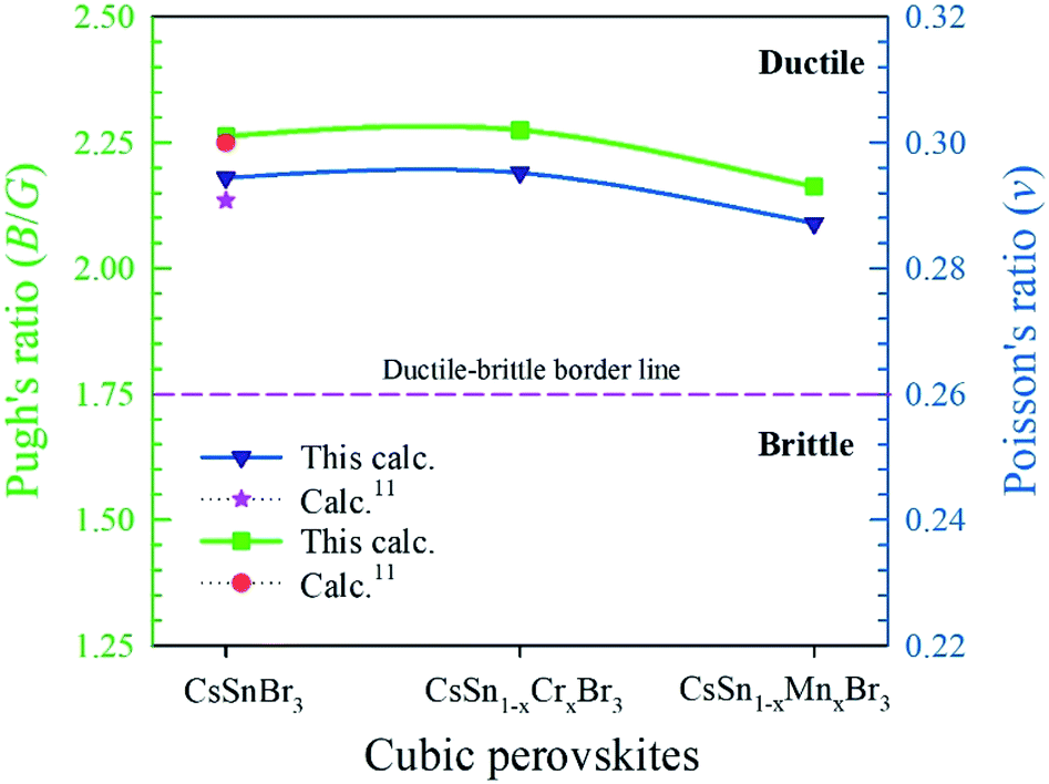 | ||
| Fig. 8 Variations of Pugh's ratio and Poisson's ratio values of pristine and metal-alloyed CsSnBr3. | ||
3.5. Significance of metal alloying in lead-free perovskites
Lead-free perovskite materials with a high absorption and high conductivity are significantly preferred in solar cells and other optoelectronic applications. These characteristics have been found in CsGeI3, which was suggested in the theoretical literature.11 However, CsGeI3 has not been previously considered in practical device applications owing to its brittle nature. On the other hand, CsGeCl3 is suggested to have a high absorption and high conductivity in a theoretical study,18 but the material reaches the critical value (0.26) for a ductile and brittle nature. Therefore, CsGeCl3 is not considered as a highly ductile material. A Ni-doped CsGeBr3 in a DFT study12 was predicted to exhibit a high absorption in the visible region. Although the peak shifts in the visible region, this peak does not reveal a high absorption compared to pure CsGeBr3. Therefore, CsGeBr3 is not highly preferable for use in solar cell devices. On the other hand, metal-doped CsGeCl3 and CsSnCl3 previously reported in the literature18,19 were suggested to possess a high absorption and high conductivity, but the reflectivity is too high compared to CsGeBr3. A reasonable value of reflectivity is highly demanded in optoelectronic devices. Another study on CsSnBr3 (ref. 11) suggests it is ductile in nature, but the material possesses a medium absorption and reduced conductivity owing to the large experimental band gap of 1.75 eV.14 Consequently, the pure form of CsSnBr3 is needed to enhance the optical, as well as the electronic, properties for use in optoelectronic applications. Alloying the material is an effective way to enhance these properties. The obtained results for metal (Cr/Mn) alloyed in CsSnBr3 in our study suggest that the high absorption and high conductivity, compared to a pristine single cell in the visible region, means its behavior is highly ductile in nature. The alloyed materials also exhibit a low value for the bulk modulus compared to the pristine samples. Therefore, materials of alloyed cases are expected to be suitable for making thin films. The observed results of the Cr- and Mn-alloyed samples indicate that the Mn-alloyed sample exhibited a greater absorption and conductivity than the Cr-alloyed sample. Our study finally suggests that Mn-alloyed CsSnBr3 is a more suitable lead-free perovskite, compared to all of the other halide perovskite materials, for use in solar cells and other optoelectronic applications.4. Conclusions
In summary, the structural, optical, electronic, and elastic properties of pure CsSnBr3 and metal (Cr/Mn) alloyed CsSnBr3 were studied using DFT. The investigated structural parameters are in good agreement with the available experimental and theoretical results. The highly ductile nature of metal-alloyed CsSnBr3 and the low value of the bulk modulus reveal its suitability for use in thin films. The wide value of the band gap of pure CsSnBr3 is not considered suitable for utilizing its solar spectrum for photovoltaic conversation; instead, the metal-alloyed samples with a narrow band gap possess higher absorption and photoconductivity and are suitable for the utilization of the solar spectrum. The Fermi levels of metal-alloyed samples shifted toward the CB, and the creation of an intermediate state helps excited photoelectrons to transfer to the CB more easily, hence enhancing the optical properties significantly. Comparative analysis of the various optoelectronic properties of pure CsSnBr3 and metal (Cr/Mn) alloyed CsSnBr3 suggests that CsSn1−xMnxBr3 was the most environmentally friendly (non-toxic) candidate for use in solar cells and for other optoelectronic applications.Conflicts of interest
The authors declare no conflicts of interest.Acknowledgements
The authors acknowledge the Department of Physics, Pabna University of Science and Technology, Bangladesh, for providing computing facilities.References
- W. Zhang, G. E. Eperon and H. J. Snaith, Nat. Energy, 2016, 1, 16048 CrossRef CAS
.
- W. J. Yin, T. Shi and Y. Yan, Adv. Mater., 2014, 26, 4653–4658 CrossRef CAS
- Q. A. Akkerman, M. Gandini, F. Di Stasio, P. Rastogi, F. Palazon, G. Bertoni, J. M. Ball, M. Prato, A. Petrozza and L. Manna, Nat. Energy, 2016, 2, 1–7 Search PubMed
- G. E. Eperon, G. M. Paterno, R. J. Sutton, A. Zampetti, A. A. Haghighirad, F. Cacialli and H. J. Snaith, J. Mater. Chem. A, 2015, 3, 19688–19695 RSC
- T. Krishnamoorthy, H. Ding, C. Yan, W. L. Leong, T. Baikie, Z. Zhang, M. Sherburne, S. Li, M. Asta, N. Mathews and S. G. Mhaisalkar, J. Mater. Chem. A, 2015, 3, 23829–23832 RSC
- P. Ramasamy, D. H. Lim, B. Kim, S. H. Lee, M. S. Lee and J. S. Lee, Chem. Commun., 2016, 52, 2067–2070 RSC
- A. Babayigit, D. D. Thanh, A. Ethirajan, J. Manca, M. Muller, H. G. Boyen and B. Conings, Sci. Rep., 2016, 6, 18721 CrossRef CAS
- G. E. Eperon, S. N. Habisreutinger, T. Leijtens, B. J. Bruijnaers, J. J. van Franeker, D. W. DeQuilettes, S. Pathak, R. J. Sutton, G. Grancini, D. S. Ginger and R. A. Janssen, ACS Nano, 2015, 9, 9380–9393 CrossRef CAS
- A. Babayigit, A. Ethirajan, M. Muller and B. Conings, Nat. Mater., 2016, 15, 247 CrossRef CAS
- S. F. Hoefler, G. Trimmel and T. Rath, Monatsh. Chem., 2017, 148, 795 CrossRef CAS
- M. Roknuzzaman, K. K. Ostrikov, H. Wang, A. Du and T. Tesfamichael, Sci. Rep., 2017, 7, 14025 CrossRef
- M. N. Islam, M. A. Hadi and J. Podder, AIP Adv., 2019, 9, 125321 CrossRef
- T. C. Jellicoe, J. M. Richter, H. F. Glass, M. Tabachnyk, R. Brady, S. E. Dutton, A. Rao, R. H. Friend, D. Credgington, N. C. Greenham and M. L. Böhm, J. Am. Chem. Soc., 2016, 138, 2941–2944 CrossRef CAS
- L. Peedikakkandy and P. Bhargava, RSC Adv., 2016, 6, 19857–19860 RSC
- M. Coduri, T. A. Strobel, M. Szafranski, A. Katrusiak, A. Mahata, F. Cova, S. Bonomi, E. Mosconi, F. De Angelis and L. Malavasi, J. Phys. Chem. Lett., 2019, 10, 7398–7405 CrossRef CAS
- Q. Mahmood, M. Yaseen, M. Hassan, M. S. Rashid, I. Tlili and A. Laref, Mater. Res. Express, 2019, 6, 045901 CrossRef
- M. G. Brik, Solid State Commun., 2011, 151, 1733–1738 CrossRef CAS
- M. Z. Rahaman and A. K. M. A. Hossain, RSC Adv., 2018, 8, 33010–33018 RSC
- J. Islam and A. K. M. A. Hossain, RSC Adv., 2020, 10, 7817–7827 RSC
- P. Hohenberg and W. Kohn, Phys. Rev. [Sect.] B, 1964, 136, 864 CrossRef
- W. Kohn and L. J. Sham, Phys. Rev. [Sect.] A, 1965, 140, 1133 CrossRef
- S. J. Clark, M. D. Segall, C. J. Pickard, P. J. Hasnip, M. I. Probert, K. Refson and M. C. Payne, Z. Kristallogr., 2005, 220, 567 CAS
- D. Vanderbilt, Phys. Rev. B: Condens. Matter Mater. Phys., 1990, 41, 7892 CrossRef
- J. P. Perdew, K. Burke and M. Ernzerhof, Phys. Rev. Lett., 1996, 77, 3865 CrossRef CAS
- H. J. Monkhorst and J. D. Pack, Phys. Rev. B, 1976, 13, 5188 CrossRef
- T. H. Fischer and J. Almlof, J. Phys. Chem., 1992, 96, 9768–9774 CrossRef CAS
- F. D. Murnaghan, Am. J. Math., 1937, 59, 235 CrossRef
- M. I. Kholil, M. S. Ali and M. Aftabuzzaman, J. Alloys Compd., 2018, 740, 754–765 CrossRef CAS
- R. D. Shannon, Acta Crystallogr., Sect. A: Cryst. Phys., Diffr., Theor. Gen. Crystallogr., 1976, 32, 751 CrossRef
- J. Barrett, S. R. A. Bird, J. D. Donaldson and J. Silver, J. Chem. Soc. A, 1971, 3105–3108 RSC
- W. Yu, J. Zhang and T. Peng, Appl. Catal., B, 2016, 181, 220–227 CrossRef CAS
- X. Zong, C. Sun, H. Yu, Z. G. Chen, Z. Xing, D. Ye, G. Q. Lu, X. Li and L. Wang, J. Phys. Chem. C, 2013, 117, 4937–4942 CrossRef CAS
- X. Liu, B. Xie, C. Duan, Z. Wang, B. Fan, K. Zhang, B. Lin, F. J. Colberts, W. Ma, R. A. Janssen and F. Huang, J. Mater. Chem. A, 2018, 6, 395–403 RSC
- M. Roknuzzaman, K. K. Ostrikov, K. C. Wasalathilake, C. Yan, H. Wang and T. Tesfamichael, Org. Electron., 2018, 59, 99–106 CrossRef CAS
- H. Lu and X. Meng, Sci. Rep., 2015, 5, 16939 CrossRef CAS
- H. Ayatullahah, G. Murtaza, S. Muhammad, S. Naeem, M. N. Khalid and A. Manzar, Acta Phys. Pol., A, 2013, 124, 102–107 CrossRef
- S. Körbel, M. A. Marques and S. Botti, J. Mater. Chem. C, 2016, 4, 3157–3167 RSC
- A. D. Becke, J. Chem. Phys., 1993, 98, 1372 CrossRef CAS
- F. Aryasetiawan and O. Gunnarsson, Rep. Prog. Phys., 1998, 61, 237 CrossRef CAS
- A. K. Singh, A. Janotti, M. Scheffl er and C. G. Van de Walle, Phys. Rev. Lett., 2008, 101, 055502 CrossRef
- M. Born, Math. Proc. Cambridge Philos. Soc., 2008, 36, 160 CrossRef
- D. G. Pettifor, Mater. Sci. Technol., 1992, 8, 345–349 CrossRef CAS
- R. Hill, Proc. Phys. Soc., London, Sect. A, 1952, 65, 349 CrossRef
- M. I. Kholil and M. T. H. Bhuiyan, Results Phys., 2019, 12, 73–82 CrossRef
- M. I. Kholil and M. T. H. Bhuiyan, Solid State Commun., 2020, 322, 114053 CrossRef CAS
- S. F. Pugh, Philos. Mag., 1954, 45, 823–843 CAS
| This journal is © The Royal Society of Chemistry 2020 |