
 Open Access Article
 This Open Access Article is licensed under a Creative Commons Attribution-Non Commercial 3.0 Unported Licence
Violet-light stimulated synaptic and learning functions in a zinc–tin oxide photoelectric transistor for neuromorphic computation†
Ting-Ruei Lin,
Li-Chung Shih,
Po-Jen Cheng,
Kuan-Ting Chen and
Jen-Sue Chen *
*
Department of Materials Science and Engineering, National Cheng Kung University, Tainan 70101, Taiwan. E-mail: jenschen@ncku.edu.tw
First published on 23rd November 2020
Abstract
In contrast to the commonly present UV light-stimulated synaptic oxide thin-film transistors, this study demonstrates a violet light (wavelength of 405 nm) stimulated zinc–tin oxide (ZTO) photoelectric transistor for potential application in optical neuromorphic computation. Owing to the light-induced oxygen vacancy ionization and persistent photoconductivity effect in ZTO, this device well imitates prominent synaptic functions, including photonic potentiation, electric depression, and short-term memory (STM) to long-term memory (LTM) transition. A highly linear and broad dynamic range of photonic potentiation can be achieved by modulating the light power density, while electric depression is realized by gate voltage pulsing. In addition, the brain-like re-learning experience with extended forgetting time (200 s) is well mimicked by the ZTO photoelectric transistor. As a result, the ZTO photoelectric transistor provides excessive synaptic function with multi-series of synaptic weight levels (90 levels for each given light power density), which makes it prevalent in the neuromorphic computation of massive data as well as in learning-driven artificial intelligence computation.
Introduction
Computers based on the von Neumann architecture have been successfully developed for solving well-structured mathematical problems during the past several decades.1 However, physically separated memory modules and processers of von Neumann-based computational systems are not suitable for solving unstructured and large quantities of data.2 In order to overcome this issue, a new type of neuromorphic computation architecture, namely artificial neural networks (ANN) has been built.3,4 Inspired by the human brain, the transmission between adjacent neurons in ANN is dependent on the synaptic weights, which are the basis for conveying information, processing data, and memory in neuromorphic systems.5 ANN-based computational systems can therefore simultaneously process and store information of large quantities of unstructured data.In contrast to purely electrically trigged synaptic devices,6–9 the photoelectric synaptic devices can be triggered by a series of UV light spikes or electric spikes,10–13 where In2O3/ZnO heterojunction, indium gallium zinc oxide (IGZO)11–15 and indium zinc oxide (IZO)16 are used as active layers. Although the reported research works are applaudable, these devices are limited to UV light stimuli to intimate synaptic functions. While visible light communication (VLC) is a potential future technology, violet light has been demonstrated to carry a high transmission capacity beyond 25 Gbit s−1.17 In addition, human eyes have a relatively low visual sensitivity to violet light. Therefore, using violet light as a source for data transmission will cause fewer disturbances to human daily life.
In this study, we have demonstrated a solution-processed zinc–tin oxide (ZTO) thin film transistor that can respond to violet light (405 nm in wavelength) stimulation and mimic the essential synaptic functions and memory behaviors based on the persistent photoconductivity (PPC) effect arising from visible light stimuli and suppression of the PPC effect with positive gate bias pulses. In addition, light-induced oxygen vacancies will replenish the oxygen vacancies for generating photoexcited electron carriers. Therefore, the degrees of photonic potentiation and electric depression are tailored by modulating the light power density and gate voltage, respectively, which provides a wide range of synaptic weight levels and makes it highly providential for the application in the neuromorphic computation of massive data.
Results and discussion
Fig. 1a shows the TEM cross-sectional image of the ZTO film deposited on SiO2, indicating that the thickness of ZTO is about 5 nm. Fig. 1b shows the transfer characteristic curves of the ZTO transistor measured in dark and under light illumination at different power densities and at a wavelength of 405 nm. The bandgap of ZTO was estimated to be 3.9 eV according to the Tauc plot converted from the UV-Vis transmission spectrum, as shown in Fig. S1 (ESI†). The XPS O1s spectrum of the ZTO film is shown in Fig. S2 (ESI†) and is deconvoluted into three components, including lattice oxygen in ZTO (530.1 eV, OI), oxygen nearby oxygen-deficient ZTO (531.8 eV, OII), and oxygen absorbed on the ZTO surface (532.6 eV, OIII).18 The OII subpeak in the XPS O1s spectrum indicates the presence of oxygen vacancies in the ZTO film. When ZTO is illuminated by a sub-bandgap light source, neutral oxygen vacancies will be photo-ionized to positively-charged oxygen vacancies and release electrons to the conduction band of ZTO.19 As a result, the negative shift of transfer characteristic curves shown in Fig. 1b is dominated by a positively electric field produced by the positively-charged oxygen vacancies mainly located at the ZTO/SiO2 interface.20 The photoelectrons released to the conduction band of ZTO will cause an increase in the conductivity of the ZTO phototransistor.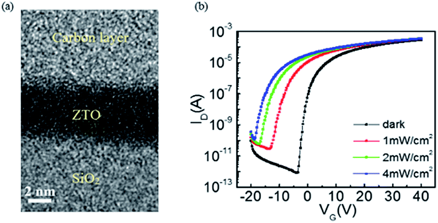 | ||
| Fig. 1 (a) TEM cross-sectional image of the ZTO film deposited on SiO2. (b) Transfer characteristic curves of the ZTO phototransistor in dark and under light illumination of 405 nm wavelength light of different power densities (VD = 10 V). | ||
As discussed in the literature,14 positively-charged oxygen vacancies take a long time to recombine with photoelectrons owing to the existence of the thermal activation energy, thus leading to the persistent photoconductivity (PPC) effect. In previous reports, the thermal activation energy for the neutralization of ionized oxygen vacancies in ZnO-based oxide is mostly found to be in the range from 0.27 eV to 0.37 eV.14,21,22 By measuring the temperature-dependent photocurrent decay time constant for the ZTO transistor under 405 nm light illumination, the thermal activation energy for the neutralization of ionized oxygen vacancies of ZTO is related to the decay time constant, τdecay, by the Arrhenius equation.
 | (1) |
![[thin space (1/6-em)]](https://www.rsc.org/images/entities/char_2009.gif) τ vs. 1/T plot shown in Fig. S3 (ESI†), the thermal activation energy for the neutralization of the ionized oxygen vacancies of ZTO can be obtained by fitting the Arrhenius plot and is calculated as 0.294 eV, which is consistent with the literature data.
τ vs. 1/T plot shown in Fig. S3 (ESI†), the thermal activation energy for the neutralization of the ionized oxygen vacancies of ZTO can be obtained by fitting the Arrhenius plot and is calculated as 0.294 eV, which is consistent with the literature data.
A schematic of biological presynaptic neurons, postsynaptic neurons, synapse and operation concept of the ZTO neuromorphic phototransistor are shown in Fig. 2a, where the information will be conveyed from presynaptic neurons to postsynaptic neurons through synapses. To intimate the biological synapses, the light spike, the positive gate bias pulse and the drain current (photo-induced current) are represented as the excitatory presynaptic neuron spike, the inhibitory presynaptic neuron spike, and the postsynaptic current, respectively. The change in the drain current (i.e. change in conductivity) thus can be represented as synaptic weight. Fig. 2b shows the typical excitatory postsynaptic current (EPSC) of the ZTO phototransistor stimulated by a single light spike (405 nm, 2 mW cm−2) with different light spike durations at VD of 10 V and VG of 0 V. EPSC increases linearly with the increase in the spike duration, which is indicative of the proportional ionization of neutral oxygen vacancies to the light spike duration. Fig. 2c shows the EPSC variation of the ZTO phototransistor under 405 nm laser light spikes with different power densities and light spike durations. It is apparent that the light-stimulated ESPC of the ZTO phototransistor can be modulated broadly, which is associated with a wide range of synaptic weights for neuromorphic computing applications.
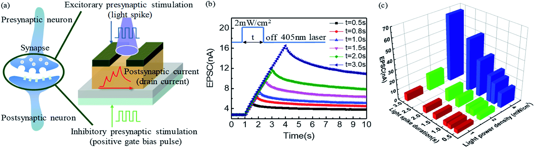 | ||
| Fig. 2 (a) A schematic of a biological presynaptic neuron, postsynaptic neuron, synapse and operation concept of the ZTO neuromorphic phototransistor. (b) EPSC of the ZTO phototransistor stimulated by a single light spike (405 nm, 2 mW cm−2) of different spike durations with VD of 10 V and VG of 0 V. (c) EPSC variation of the ZTO phototransistor triggered by 405 nm light spikes with different power densities and light spike durations. | ||
Based on the memory level and retention time, human memory behavior can be categorized into two types: short-term memory (STM) and long-term memory (LTM).23 STM is recognized as the temporal memory stimulated by external stimulation and will forget immediately (low memory level and short retention time). LTM is recognized as the enduring memory stimulated by external spike and will forget slowly (high memory level and long retention time). With maintaining the rehearsal of stimulation, STM can be transformed into LTM. In order to investigate the memory behaviors, a series of light spikes (spike duration and interval are 0.5 s) are applied to the ZTO phototransistor. The post-synaptic current responses of the ZTO phototransistor to 405 nm light spikes of different power densities (1, 2 and 4 mW cm−2) for up to 90 spikes are shown in Fig. S4 (ESI†), and the data pertaining to the light power of 2 mW cm−2 is plotted in Fig. 3a. As shown in Fig. S4† and 3a, EPSC increases continuously without saturation under each light spike. The good linearity and wide dynamic synaptic weight range of this device are superior to other reported data and will be discussed later (see Table 1). On the other hand, the forgetting behavior (decay of EPSC after the light pulse section is finished) can be described by24
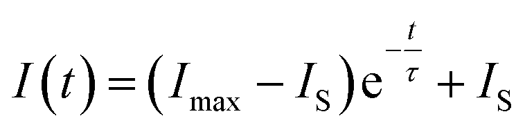 | (2) |
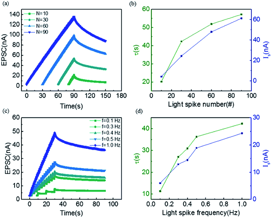 | ||
| Fig. 3 (a) EPSC of the ZTO phototransistor responses to 405 nm light spikes of different spike numbers (P = 2 mW cm−2, spike duration = 0.5 s, VD = 10 V and VG = 0 V). The STM-to-LTM transition induced by increasing the number of light spikes (405 nm, P = 2 mW cm−2, spike duration is 0.5 s, spike interval is 0.5 s) with VD of 10 V and VG of 0 V of the ZTO phototransistor. (b) The variations in the retention time and memory level with the light spike number. (c) EPSC of the ZTO phototransistor responses to light spikes of different frequencies (405 nm, P = 2 mW cm−2, spike duration = 0.5 s, VD = 10 V and VG = 0 V). (d) The variations in the retention time and memory level with the light spike frequency. | ||
| Device structure | Light source and light power density (for synaptic functions) | α | Multi-level states | Dynamic range | |
|---|---|---|---|---|---|
| Imax/I1 | Imax − I1 (nA) | ||||
| Mo/IGZO/nanogranular SiO2/p+-Si12 | 395 nm UV | ||||
| P = 158.62 mW cm−2 | 75 | 20 | 1.04 | 0.35 | |
| Au/Ti/IGZO/Al2O3/n+-Si13 | 380 nm UV | ||||
| P = 0.6 mW cm−2 | 1.2 | 20 | 12.58 | 0.21 | |
| IZO/IGZO/SiO2/Si14 | 380 nm UV | ||||
| P = 0.6 mW cm−2 | 0.8 | 30 | 42.44 | 121.30 | |
| Au/Ti/IGZO/HfOx/Au/SiO2/Si15 | 254 nm UV | ||||
| P = 0.2 mW cm−2 | 0.7 | 27 | 62.84 | 295.29 | |
| Al/IZO/ion gel/Al16 | 275 nm UV | ||||
| P = 1.82 mW cm−2 | 5 | 50 | 1.82 | 5.62 | |
| Al/ZTO/SiO2/p+-Si (this work) | 405 nm visible | ||||
| P = 1 mW cm−2 | 1.17 | 90 | 11.62 | 50.13 | |
| P = 2 mW cm−2 | 1.07 | 90 | 25.64 | 130.70 | |
| P = 4 mW cm−2 | 1.10 | 90 | 52.75 | 527.80 | |
By fitting the experimental data (Fig. 3a) with eqn (2), the retention time (τ) and memory level (IS) are obtained as shown in Fig. 3b. An increase in the retention time and memory level with light spike number confirms that the ZTO phototransistor can undergo a transition from STM to LTM such as the human brain. Apart from increasing the light spike number, increasing the light spike frequency is also an effective way to mimic the transition from STM to LTM. An increase in EPSC after different spike frequencies are shown in Fig. 3c. During the measurement, the power density of light spikes and spike duration are 2 mW cm−2 and 0.5 s, respectively. The retention time and memory level at different light spike frequencies are shown in Fig. 3d, which clearly exhibits the transition from STM to LTM via increasing light spike frequency.
The prolonged retention time of EPSC when the ZTO phototransistor is stimulated with the increase in the light spike number or frequency indicates that the PPC effect becomes stronger with cumulative photon doses. In investigations on the PPC effect of n-GaAs25 and II–V mixed semiconductors,26 it has been reported that both PPC build-up level and decay time increased with an increase in the dose of irradiated photons. Theoretical studies suggested that photo-generated electrons and holes were spatially separated and the holes were trapped (or localized), leading to the impediment of photo-generated carrier recombination. As discussed previously, the PPC effect in ZnO-based oxides originates from the energy barrier for the recombination of photo-ionized oxygen vacancies with photoelectrons. The photo-ionized oxygen vacancies are localized in the lattices; therefore, it is reasonable to postulate that the photoelectrons and photo-ionized oxygen vacancies in ZTO are also spatially separated. As a consequence, the PPC effect of the ZTO phototransistor can be enhanced with cumulative photon dose and the STM-to-LTM transition can be emulated by increasing the number or frequency of light spike stimuli.
The learning-experience of the human brain has also been intimated by the ZTO phototransistor with three cycles of learning-and-forgetting, as shown in Fig. 4a–f. In the first learning process, EPSC increases linearly after each light spike. In the first forgetting process, EPSC gradually decays to an intermediate state after 200 s. This is analogous to the human brain, where the information will be partially lost after a period of time. Compared to the 18 spikes in the first-learning process, only 8 and 7 spikes are required for the second and third learning processes, respectively, to recover the decayed EPSC. In addition, during the second and third forgetting processes, the decay of EPSC is comparatively less than that for the first forgetting process within the same period (200 s). Similar to the human brain, when the same information is relearnt, we can learn faster and retain it for a longer time (less forgotten). As a result, the ZTO phototransistor imitates the learning-forgetting-relearning behavior of the human brain agreeably.
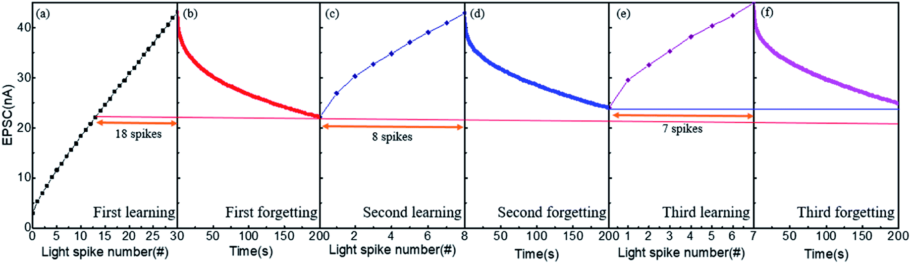 | ||
| Fig. 4 Learning-experience behavior in the ZTO phototransistor (learning process: 405 nm light, P = 2 mW cm−2, light spike duration and interval are 0.5 s, VD = 10 V and VG = 0 V; forgetting process: VD = 10 V and VG = 0 V) (a) first learning process, (b) first forgetting process, (c) second learning process, (d) second forgetting process, (e) third learning process, (f) third forgetting process. | ||
The photonic potentiation behavior associates with the PPC effect of the ZTO phototransistor indicates the strengthening of the synaptic weight. On the contrary, the depression behavior must be accompanied by the elimination of PPC of the ZTO phototransistor, representing the weakening of the synaptic weight. As suggested in the literature,19,21 by applying positive gate bias pulses, photoelectrons will accumulate at the front channel to accelerate the recombination rate of photoelectrons and photo-ionized oxygen vacancies. Fig. 5a–c reveal the various degrees of electric depression by modulating the positive gate voltage after photonic potentiation with different light power densities. Accordingly, the ZTO phototransistor can provide a wide range of synaptic weights for neuromorphic computing under different light power densities, spike numbers and positive gate bias voltages.
 | ||
| Fig. 5 Photonic potentiation (405 nm, light spike duration and interval are 0.5 s, spike number is 30) under light power density of (a) 1 mW cm−2 (b) 2 mW cm−2 (c) 4 mW cm−2 and the subsequent electrical depression (gate bias is 5 V/10 V/15 V, pulse width and interval are 0.5 s, pulse number is 60) for the ZTO phototransistor. | ||
The accuracy of the neuromorphic computation is dependent on the linearity during potentiation, multilevel states (i.e. number of synaptic weights), and dynamic range (Imax/I1 and Imax − I1, where I1 is the current at the first light spike).27 To effectively compare the linearity during potentiation, we employed the parameter α defined in the following equation.28
| I = ((Imaxα − Idarkα) × ω + Idarkα)1/α if α ≠ 0, I = Idark × (Imax/Idark)ω if α = 0 | (3) |
The comparisons of these synaptic performances between the ZTO phototransistor and previously reported oxide TFTs are summarized in Table 1. It is worth noting that our phototransistor is operated in the visible light region (violet, 405 nm) and the previously reported oxide TFT photoelectronic synapses are applied in the UV light region (254–395 nm). The dynamic range of Imax/I1 for our phototransistors may be smaller than that of some other devices operated with UV light of comparable power densities, which can be reasoned from the smaller photon energy of purple light. From Table 1, it is clear that our ZTO phototransistor has good linearity (α = ∼1) and a rather wide dynamic range, particularly on the Imax − I1 values, during photonic potentiation, and provides substantially more synaptic weight levels than those for previously reported synaptic phototransistors. The good linearity and wide dynamic synaptic weight range indicate that the photo-induced electrical current of our ZTO phototransistor will not saturate easily. It can be explained by the light-induced oxygen vacancy generation, which has been reported for the interaction of light with the ZnO surface.29 Because the thickness of our ZTO film is only 5 nm, the light interaction with the ZTO surface will be dominant. The light-induced oxygen vacancies will thus replenish the neutral oxygen vacancies, which have been photo-ionized to generate photoexcited electron carriers. Consequently, a significantly high number of synaptic weight levels can be realized. The light potentiation and gate bias depression synaptic performances of ZTO phototransistors, therefore, are very promising for next-generation neuromorphic computing applications. It is worth noting that in addition to serving as the active layer ZnO can also be the charge trapping medium in the organic–inorganic hybrid transistor, which exhibited quadruple (400%) change in synaptic weight within 10 optical (UV light) pulses.30
Conclusions
In summary, by applying violet light spikes and gate voltage pulses, prominent synaptic functions and memory behaviors, including potentiation, depression, STM-to-LTM transition and learning experience, are well imitated by the ZTO photoelectric neuromorphic transistor. The photonic potentiation process in the ZTO phototransistor is associated with the PPC effect, resulting from the activation energy barrier for the recombination of ionized oxygen vacancies with electrons, while the electric depression process is attained by applying positive gate bias pulses to annihilate the PPC effect. Owing to the light-induced oxygen vacancy generation and ultra-thin ZTO thickness, under sequential light spikes, the excitatory postsynaptic current (EPSC) of the ZTO phototransistor increases continuously and linearly with spike number up to at least 90, and the dynamic range of EPSC can be further modified by light power density. Therefore, the synaptic operation of the ZTO phototransistor provides an extensive series of weight levels and makes it suitable to process large quantities of data for next-generation neuromorphic computing.Experimental
In this study, the ZTO precursor solution for the active layer was prepared by dissolving tin chloride and zinc acetate precursors (molar ratio of Zn:Sn = 1:1) in the solvent of 2-methoxyethanol. The ZTO solution was spin-coated onto the SiO2 (110 nm)/p+-Si substrate, followed by a heat treatment at 500 °C for 1 h. The p+-Si substrate serves as the gate electrode and SiO2 is the gate dielectric layer. After annealing, the ZTO thin film was patterned by photolithography. Finally, 300 nm-thick Al was deposited by e-beam evaporation using a shadow mask to define the source/drain electrodes. The channel width and channel lengths were 2000 μm and 100 μm, respectively.
Transmission electron microscopy (TEM) images on ZTO were obtained using a JEM 2100F field emission transmission electron microscope. The chemical bonding states of the ZTO film were examined by X-ray photoelectron spectroscopy (XPS, JEOL JAMP-9500F) with a monochromatic Al Kα source. Electrical characteristics of the ZTO photoelectric transistor were measured using an Agilent 4156C semiconductor parameter analyzer. For the violet light illumination, 405 nm laser (SDL-405-LM-010T) was used as light sources during photo-electrical measurement and all measurements were performed in a dark box.
Conflicts of interest
There are no conflicts to declare.Acknowledgements
We appreciate the financial support from the Ministry of Science and Technology of Taiwan (Project No. MOST 109-2221-E-006-114-MY3 and MOST 109-2224-E-006-009).References
- J. von Neumann, Ann. Hist. Comput., 1989, 10, 243–256 Search PubMed.
- P. A. Merolla, J. V. Arthur, R. Alvarez-Icaza, A. S. Cassidy, J. Sawada, F. Akopyan, B. L. Jackson, N. Imam, C. Guo, Y. Nakamura, B. Brezzo, I. Vo, S. K. Esser, R. Appuswamy, B. Taba, A. Amir, M. D. Flickner, W. P. Risk, R. Manohar and D. S. Modha, Science, 2014, 345, 668–673 CrossRef CAS.
- G. Indiveri and T. K. Horiuchi, Front. Neurosci., 2011, 5, 118 Search PubMed.
- R. Sarpeshkar, Brain power, IEEE Spectrum, 2006, 43, 24–29 Search PubMed.
- D. Ielmini and S. Ambrogio, Nanotechnology, 2020, 31, 092001 CrossRef CAS.
- K. Beom, P. Yang, D. Park, H. J. Kim, H. H. Lee, C. J. Kang and T. S. Yoon, Nanotechnology, 2019, 30, 025203 CrossRef.
- K. H. Han, G. S. Kim, J. Park, S. G. Kim, J. H. Park and H. Y. Yu, ACS Appl. Mater. Interfaces, 2019, 11, 20949–20955 CrossRef CAS.
- H. C. Zhu, H. J. Mu, Z. Y. Cai, X. F. Chu and X. T. Yang, Phys. Status Solidi A, 2019, 1900344 CrossRef.
- Y. He, R. Liu, S. Jiang, C. Chen, L. Zhu, Y. Shi and Q. Wan, J. Phys. D: Appl. Phys., 2020, 53, 215106 CrossRef CAS.
- M. Kumar, S. Abbas and J. Kim, ACS Appl. Mater. Interfaces, 2018, 10, 34370–34376 CrossRef CAS.
- Y. L. He, S. Nie, R. Liu, S. S. Jiang, Y. Shi and Q. Wan, IEEE Electron Device Lett., 2019, 40, 818–821 CAS.
- W. J. Cheng, R. R. Liang, H. Tian, C. C. Sun, C. S. Jiang, X. W. Wang, J. Wang, T. L. Ren and J. Xu, IEEE J. Electron Devices Soc., 2019, 7, 38–45 CAS.
- H. K. Li, T. P. Chen, P. Liu, S. G. Hu, Y. Liu, Q. Zhang and P. S. Lee, J. Appl. Phys., 2016, 119, 244505 CrossRef.
- M. Lee, W. Lee, S. Choi, J. W. Jo, J. Kim, S. K. Park and Y. H. Kim, Adv. Mater., 2017, 29, 1700951 CrossRef.
- Q. T. Wu, J. W. Wang, J. C. Cao, C. Y. Lu, G. H. Yang, X. W. Shi, X. C. Chuai, Y. X. Gong, Y. Su, Y. Zhao, N. D. Lu, D. Geng, H. Wang, L. Li and M. Liu, Adv. Electron. Mater., 2018, 4, 1800556 CrossRef.
- J. X. Wang, Y. Chen, L. A. Kong, Y. Fu, Y. L. Gao and J. Sun, Appl. Phys. Lett., 2018, 113, 151101 CrossRef.
- W.-C. Wang, H.-Y. Wang and G.-R. Lin, Sci. Rep., 2018, 8, 13142 CrossRef.
- K.-H. Lim, K. Kim, S. Kim, S. Y. Park, H. Kim and Y. S. Kim, Adv. Mater., 2013, 25, 2994–3000 CrossRef CAS.
- S. Jeon, S. E. Ahn, I. Song, C. J. Kim, U. I. Chung, E. Lee, I. Yoo, A. Nathan, S. Lee, K. Ghaffarzadeh, J. Robertson and K. Kim, Nat. Mater., 2012, 11, 301–305 CrossRef CAS.
- J. G. Um, M. Mativenga and J. Jang, Appl. Phys. Lett., 2013, 103, 033501 CrossRef.
- K. Ghaffarzadeh, A. Nathan, J. Robertson, S. Kim, S. Jeon, C. Kim, U. I. Chung and J. H. Lee, Appl. Phys. Lett., 2010, 97, 143510 CrossRef.
- S. E. Ahn, I. Song, S. Jeon, Y. W. Jeon, Y. Kim, C. Kim, B. Ryu, J. H. Lee, A. Nathan, S. Lee, G. T. Kim and U. I. Chung, Adv. Mater., 2012, 24, 2631–2636 CrossRef CAS.
- J. L. McGaugh, Science, 1966, 153, 1351–1358 CrossRef CAS.
- T. Chang, S.-H. Jo and W. Lu, ACS Nano, 2011, 5, 7669–7676 CrossRef CAS.
- H. J. Queisser and D. E. Theodorou, Phys. Rev. Lett., 1979, 43, 401–404 CrossRef CAS.
- H. X. Jiang, J. Y. Lin and J. Y. Percolation, Phys. Rev. Lett., 1990, 64, 2547–2550 CrossRef CAS.
- D. Kuzum, S. M. Yu and H. S. P. Wong, Nanotechnology, 2013, 24, 382001 CrossRef.
- S. Lim, M. Kwak and H. Hwang, IEEE Trans. Electron Devices, 2018, 65, 3976–3981 CAS.
- R. Gurwitz, R. Cohen and I. Shalish, J. Appl. Phys., 2014, 115, 033701 CrossRef.
- J.-Y. Mao, L. Hu, S.-R. Zhang, Y. Ren, J.-Q. Yang, L. Zhou, Y.-J. Zeng, Y. Zhou and S.-T. Han, J. Mater. Chem. C, 2019, 7, 48–59 RSC.
Footnote |
| † Electronic supplementary information (ESI) available: UV-Vis transmission and XPS spectra et al. See DOI: 10.1039/d0ra08777g |
| This journal is © The Royal Society of Chemistry 2020 |