DOI:
10.1039/D0RA08405K
(Paper)
RSC Adv., 2020,
10, 42542-42556
Structural, optical and dielectric properties of Cu1.5Mn1.5O4 spinel nanoparticles
Received
1st October 2020
, Accepted 4th November 2020
First published on 23rd November 2020
Abstract
In this study, a Cu1.5Mn1.5O4 spinel was successfully synthesized by a sol–gel method at 500 °C for 5 h and characterized by different techniques. X-ray diffraction (XRD), Fourier transformation infrared (FTIR) spectroscopy and Raman spectroscopic analyses confirmed the formation of a spinel cubic structure with the Fd![[3 with combining macron]](https://www.rsc.org/images/entities/char_0033_0304.gif) m space group. The SEM proves that the grain size of our compound is of the order of 48 nm. Crystallite sizes determined from three estimates are closer to the grain size obtained from the SEM, indicating the single domain nature of the sample. The optical properties of UV-visible spectroscopy for our sample showed that the gap value is equal to 3.82 eV, making our compound a good candidate for optoelectronic applications. For electrical properties, impedance spectroscopy was performed at a frequency range of 40 ≤ frequency ≤ 106 Hz. This suggested hoping conduction due to three theoretical models. The latter can be attributed to the correlated barrier hopping (CBH) model in region I, overlapping large polaron tunneling (OLPT) in region II and non-overlapping small polaron tunneling (NSPT) mechanism in region III. One dielectric relaxation is detected from the dielectric impedance and modulus, attributed to grain contributions. This behavior was confirmed by both Nyquist and Argand's plots of dielectric impedance at different measuring temperatures.
m space group. The SEM proves that the grain size of our compound is of the order of 48 nm. Crystallite sizes determined from three estimates are closer to the grain size obtained from the SEM, indicating the single domain nature of the sample. The optical properties of UV-visible spectroscopy for our sample showed that the gap value is equal to 3.82 eV, making our compound a good candidate for optoelectronic applications. For electrical properties, impedance spectroscopy was performed at a frequency range of 40 ≤ frequency ≤ 106 Hz. This suggested hoping conduction due to three theoretical models. The latter can be attributed to the correlated barrier hopping (CBH) model in region I, overlapping large polaron tunneling (OLPT) in region II and non-overlapping small polaron tunneling (NSPT) mechanism in region III. One dielectric relaxation is detected from the dielectric impedance and modulus, attributed to grain contributions. This behavior was confirmed by both Nyquist and Argand's plots of dielectric impedance at different measuring temperatures.
1. Introduction
During the last decade, copper manganites have attracted considerable attention in response to their properties. These materials crystallize in the spinel structure, based on the cubic close packing of oxygen ions in which cations can occupy either tetrahedral or octahedral sites. A spinel can adopt a normal, an inverse or a mixed structure. Due to these possibilities, many different spinel materials can be synthesized.1 Experimentally, the synthesis methods of spinel nanoparticles include sol–gel,2 ceramic,3 hydrothermal, co-precipitation,4 micro-emulsion,5 novel combustion,6 mechano-chemical,7 micro-wave sintering8 and two-step direct micro-emulsion procedures.9 Manganese-copper spinels exhibit a wide range of electrical properties. These properties depend on the type of ion and its position in the unit cell.10 Keeping in view the formation aspects of Cu–Mn–O complex oxides, several kinds of spinel phases such as CuMn2O4 and Cu1.5Mn1.5O4 can be formed by changing the molar ratio of copper to manganese at a certain range. The fabrication of the ternary transition metal oxide Cu1.5Mn1.5O4 single phase is a challenge unachievable. The formation of Cu Oxide secondary phases in small percentages is more likely to take place during the synthesis process. Copper and manganese are less expensive and more abundant than nickel and cobalt. The spinel-type oxides, copper manganese and their composites, are receiving great attention for their numerous technological applications. The latter consist of rechargeable lithium batteries,11 catalysts,12 electrochemical biosensors,13 selective sun absorbers (in solar thermal energy conversion systems),14,15 collectors, and anti-corrosion coatings, given their excellent structural, chemical and physical properties. The physicochemical properties of copper manganese spinel-type mixed oxides are mainly determined in terms of the charge, type and distribution in the tetrahedral/octahedral sites of the cations.16 Literature searches of the theoretical and experimental studies17–19 revealed that the research problem regarding Cu1.5Mn1.5O4 has been addressed so far to characterize their structural, catalytic and optical properties. Thus far, the dielectric property is under-examined and needs further research. The temperature coefficient of resistivity (TCR) is an important variable for sensor material performance used in an uncooled IR bolometer, as defined by the equation TCR = [(1/ρ) × (dρ/dT)] × 100%.20 Literature review revealed that numerous types of thermistor materials have been widely investigated.21–23 These materials are spinel ternary transition metal oxides of copper, nickel, manganese, and cobalt (Cu, Ni, Mn, Co–O) with a general formula AB2O4. They have been extensively investigated in terms of uncooled IR detection and its high negative TCRs (≤3.5%/K), moderate resistance and long-term stability.24,25 The present work aims at synthesizing and characterizing the spinel nanoparticle Cu1.5Mn1.5O4 by the sol–gel method. The results of the experimental and theoretical phases regarding the structural, optical, and dielectric properties are outlined and discussed. The present paper provides the research with a full image of the spinel oxide behavior that may serve various applications.
2. Experimental details
2.1. Synthesis of Cu1.5Mn1.5O4 nanoparticles
All the chemical reactants used in the present work were purchased from Sigma-Aldrich and used without further purification. The nanoparticle Cu1.5Mn1.5O4 was prepared by the sol–gel method.26 Generally, the precursors used are nitrates along with a mixture of nitrates-oxides. For the preparation of our compound, the nitrates used were [Cu(NO3)2·3H2O, Mn(NO3)2·4H2O], the purity of which was 99.9%. This method's principle is to weigh the precursors at the desired stoichiometric proportions using a precision balance. The latter was dissolved in distilled water at room temperature, followed by the addition of citric acid [C6H8O7] (with a molar ratio of 1![[thin space (1/6-em)]](https://www.rsc.org/images/entities/char_2009.gif) :1.5 of metal cation (Mn + Cu) to citric acid) and ethylene glycol [C2H6O2] used as a gelling agent. The same method also aims to maintain the reaction's transparency and homogeneity. The mixture obtained was then heated to 70–80 °C on a hot plate for a few hours while continuing to eliminate the excess of water and form a viscous gel. Subsequently, the temperature was raised to 300 °C to ensure the combustion responsible for transforming the gel into a fine powder. The powders obtained were pelletized and annealed at 500 °C for 5 hours in air and cooled slowly at room temperature in order to crystallize our compound and to eliminate the excess of residual organic matter.
:1.5 of metal cation (Mn + Cu) to citric acid) and ethylene glycol [C2H6O2] used as a gelling agent. The same method also aims to maintain the reaction's transparency and homogeneity. The mixture obtained was then heated to 70–80 °C on a hot plate for a few hours while continuing to eliminate the excess of water and form a viscous gel. Subsequently, the temperature was raised to 300 °C to ensure the combustion responsible for transforming the gel into a fine powder. The powders obtained were pelletized and annealed at 500 °C for 5 hours in air and cooled slowly at room temperature in order to crystallize our compound and to eliminate the excess of residual organic matter.
2.2. Characterizations
The phase composition of the prepared sample was studied by powder X-ray diffraction (XRD) using a Bruker D8 diffractometer with Cu Kα radiation (λ = 1.5406 Å). The morphologies and sizes of the samples were directly investigated by Merlin scanning electron microscopy (SEM) at an accelerating voltage of 3 kV equipped with an energy-dispersive X-ray spectrometer (EDXS) employed for the elemental analysis of the various phases. The infrared spectra of the powders (as pellets in KBr) were recorded using a Thermo Scientific Nicolet 6700 FTIR Spectrometer at room temperature by diffuse reflectance infrared Fourier transform spectroscopy (DRIFTS) technique in the range of 400 to 4000 cm−1. The Raman spectra were recorded using a SENTERRA spectrometer (Bruker, Germany) at room temperature with laser excitation at 532 nm. Then, the UV-vis absorption spectra were recorded using a UV-vis spectrophotometer (SHIMADZU, Japan) for the UV/visible/IR range. For electrical measurements, a thin silver film was deposited through a circular mask of 8 mm diameter on both sides of the pellet. A plane capacitor configuration was obtained, making it possible to investigate the synthesized material's electrical properties. Measurements were conducted using an Agilent 4294A analyzer under vacuum with a signal amplitude of 20 mV. The explored range of frequency was between 40 Hz and 110 MHz. The temperature was from 80 K to 240 K.
3. Results and discussions
3.1. XRD study
Fig. 1a shows the X-ray diffraction (XRD) pattern at room temperature of Cu1.5Mn1.5O4 refined by the Rietveld method,27 using the FullProf28 software. In the refinement, the background was corrected by a pseudo-Voigt function. The oxygen positions (x = y = z) were taken as free parameters. However, all other atomic fractional positions were taken as fixed. Other parameters such as lattice constants, isothermal parameters, occupancies, scale factors, and shape parameters were taken as free parameters. The parameters related to thermal fluctuations were not refined, since their influence was negligible compared to the uncertainties introduced by the refinement of occupancy factors. The fitting between the observed and the calculated diffraction profiles shows an excellent agreement, taking into consideration the low value of the fit indicator (χ2 = 1.15). Moreover, the diffraction peaks at 2θ values of 30.48, 35.91, 37.57, 43.65, 47.80, 54.18, 57.76 and 63.45 correspond to the (220), (311), (222), (400), (331), (422), (333) and (440) crystal planes of the cubic Cu1.5Mn1.5O4 spinel structure. The result confirmed the formation of the single-phase cubic spinel structure29 with the space group Fdm with secondary phase peaks CuO designated by (*) detected at a calcination temperature of 500 °C. Ma et al.19 reported the presence of CuO phase in the Cu1.5Mn1.5O4 nanoparticle up to the annealing temperature of 900 °C. The obtained Rietveld refinement parameters of each sample are presented in Table 1. The low values of reliability factors and goodness of fit (χ2) affirm the correctness of fit and the high accuracy of refinement. The crystal structure of our compound is schematically depicted in Fig. 1b using the Vesta software.30 The distribution can be of the following formula [Cu]A [Cu0.5 Mn1.5]BO4.31 All peaks can be indexed using the cubic unit cell. The lattice parameters and cell volume of the Cu1.5Mn1.5O4 nanoparticles were extracted directly from the refinement.
 |
| | Fig. 1 X-ray diffraction pattern (a) and crystal structure (b) of Cu1.5Mn1.5O4 nanoparticles. | |
Table 1 XRD parameters calculated from the XRD patterns of Cu1.5Mn1.5O4
| Parameter |
Cu1.5Mn1.5O4 |
| a (Å) |
8.286(6) |
| V (Å3) |
569.022(1) |
| χ2 |
1.15 |
| RP (%) |
17 |
| Rwp (%) |
9.72 |
| Re (%) |
9.3 |
| LA (Å) |
3.587(9) |
| LB (Å) |
3.435(1) |
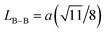
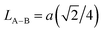
| LA–B (Å) |
2.929(9) |
| ρX-ray (g cm−3) |
5.641 |
| ρexp (g cm−3) |
5.172 |
| P (%) |
8.4 |
| S (m2 g−1) |
34.31 |
| δ (nm−2) |
1.01 × 10⁻³ |
| N (nm−2) |
28.992 |
We calculated the link lengths between the sites of the spinel structure (LA−A, LB–B and LA–B) using Standely's equations as follows:32
| |
 | (1) |
| |
 | (2) |
| |
 | (3) |
X-ray density (
ρX-ray) was calculated taking into consideration that a basic unit cell of the cubic spinel structure contained eight ions according to the following formula:
33| |
 | (4) |
whereby 8 is the number of molecules in a unit cell of spinel lattice.
M is the molecular weight of each compound,
a is the as-calculated lattice parameter converted into centimeter units and
NA is Avogadro's number.
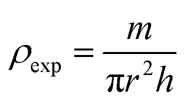
The bulk density ρexp was estimated using the following relation:34
| |
 | (5) |
where
h,
r and
m are the thickness, radius and mass of the pellet respectively.
The notion of porosity was attributed to the difference between the X-ray density and the experimental density according to the following formula:35
| |
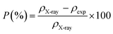 | (6) |
where
ρX-ray is the X-ray density and
ρexp is the bulk density.
Assuming all the particles are spherical, the specific surface area was calculated using the following relation:36
| |
 | (7) |
whereby the constant 6000 is a form factor for spherical particles,
DW–H is the diameter of the particle in meters (
m) calculated from the Williamson–Hall model and
ρexp is the density expressed in g m
−2.
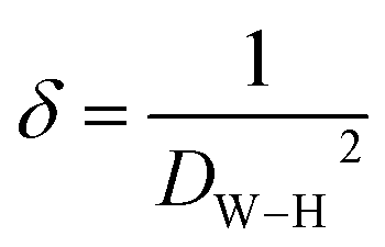
The number of defects in the sample was represented by the dislocation density (δ), which is defined as the length of the dislocation lines per unit volume of the crystal:37
| |
 | (8) |
where
DW–H is the particle diameter expressed in nm.
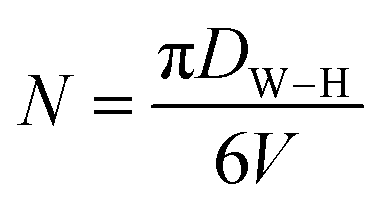
The number of unit cells (N) of Cu1.5Mn1.5O4 crystals was calculated using the following formula:
| |
 | (9) |
where
DW–H is the diameter of the particle calculated from the Williamson–Hall model and
V is the volume of the unit cell.
Lattice parameter a, volume, the link lengths between the spinel structure's sites (LA–A, LB–B et LA–B), X-ray density, experimental density, porosity, specific surface, number of defects in the sample and the number of cell units are listed in Table 1.
The notion of porosity, the specific surface area as well as the number of cell units show that the uniform particle size distribution is well agglomerated and nearly homogeneously over the entire surface of the sample. The large surface area of spinel nanoparticles is required for the detection and application of gas sensors.38
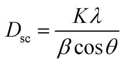
The average crystallite size Dsc was calculated from the line broadening of maximum intensity peak corresponding to the plane (311) using the Debye–Scherrer equation:39
| |
 | (10) |
where
Dsc is the crystallite size,
K is a constant of approximate value 0.9,
λ is the wavelength of the used X-ray,
β is the full width at half maximum (FWHM) of the diffraction peak and
θ is the Bragg angle for the most intense peak. The value of the crystallite size of Cu
1.5Mn
1.5O
4 corresponds to 24 nm, which confirms the nanometer size of our sample. A second estimate was obtained by the Williamson–Hall method according to the following equation:
40| |
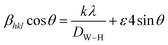 | (11) |
whereby
DW–H is the crystallite size,
k is the shape factor (0.9),
λ is the wavelength of Cu Kα radiation,
ε is a coefficient related to the strain effect on the crystallites, β is the full width at half maximum (FWHM) of each diffraction peak, and
θ is the Bragg angle for the different peaks. The W–H plot outlined in
Fig. 2a was obtained by plotting
βcos
θ against 4
sin
θ. The strain was obtained from the slope of the linearly adjusted data and the interception gave the crystallite size. The values of
DW–H and
ε were found to be respectively 31 nm and 1.14 × 10
−3. The latter displays a positive value, indicating lattice expansion.
41
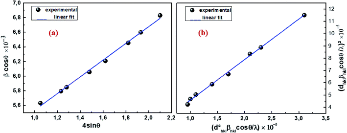 |
| | Fig. 2 W–H analysis (a) and SSP graph (b) of Cu1.5Mn1.5O4 nanoparticles. | |
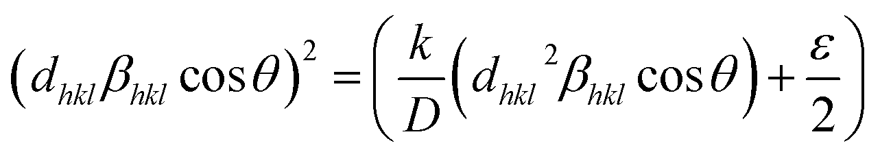
A third estimate is the size–strain plot method; it is assumed that the profile is illustrated from the “stress profile” by a Gaussian function and from the “crystallite size” by the Lorentzian function.42 Accordingly, we have the following:
| |
 | (12) |
where
K = 0.75 is a constant that depends on the shape of the particles for spherical particles,
d is the inter planer spacing,
ε is the average strain produced in the lattice,
β is the full width at half maximum (FWHM) of each diffraction peak, and
θ is the Bragg angle for the different peaks. In
Fig. 2b, (
dhkl2βhklcos
θ/
λ) and (
dhklβhklcos
θ/
λ)
2 were respectively taken as abscissa and ordinate for all Cu
1.5Mn
1.5O
4 peaks. The crystallite size
Dssp was calculated from the data adjusted linearly on the slope 26 nm and the interception gives the microstrain 3.28 × 10
−3. At first, the crystallite size calculated by the Debye–Scherrer method supports the choice of the sol–gel method for the preparation of our sample. Looking from another side, the crystallite sizes evaluated by the Williamson–Hall and size–strain plot models are slightly higher than those calculated by Scherrer's formula. The broadening effect resulting from the presence of strains is completely excluded in the Debye–Scherrer method.
43
3.2. SEM and EDX analysis
The surface morphology of the Cu1.5Mn1.5O4 spinel obtained at 500 °C was studied, and the corresponding SEM image presented in Fig. 3a shows a fairly high agglomeration of the grains, which can be attributed to electrostatic effects. The average grain size of particles presented in the inset of Fig. 3b was analyzed quantitatively by fitting the histogram using a Lorentzian function and the ImageJ software, and hence, DSEM is of the order of 48 nm. The grain size observed by the SEM is closer to the crystallite size obtained from the XRD pattern, which confirms the formation of monocrystalline particles, the sizes of which are close to the values revealed by a study on similar spinel materials.44 The chemical analysis was carried out by X-ray energy-dispersive spectroscopy (EDX). Fig. 4 shows the presence of all the constituent elements of Cu1.5Mn1.5O4, namely, oxygen (O), manganese (Mn) and copper (Cu). This was confirmed by the appearance of the characteristic peaks of these elements on the EDX spectra obtained, which then confirms the purity of the synthesized material.
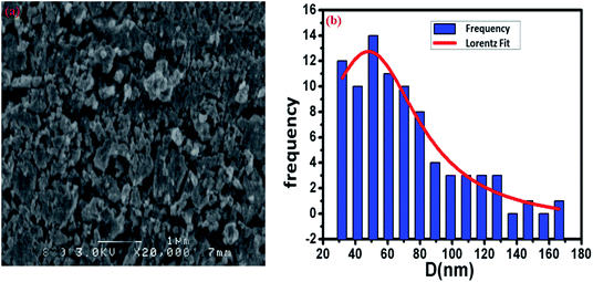 |
| | Fig. 3 SEM image (a) and size distribution histogram (b) of Cu1.5Mn1.5O4 nanoparticles. | |
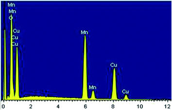 |
| | Fig. 4 Spectra of chemical analysis of Cu1.5Mn1.5O4 nanoparticles. | |
3.3. FTIR and Raman analysis
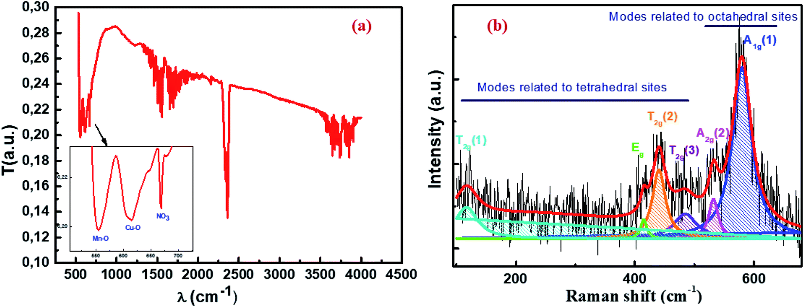
The Fourier transform infrared (FTIR) spectrum recorded in the wave number range of 400–4000 cm−1 at room temperature provides vibrational information about our material analyzed. As shown in Fig. 5a, there are two absorption bands: the first appears at 555 cm−1 and the second at 613 cm−1, indicating the presence of metal oxides.45,46 These peaks of metal–oxygen bonds are attributed respectively to the stretching vibration of the Mn–O cation–anion band47 in the octahedral (B) sites (νB) and the stretching vibration of the Cu–O cationic anionic band in the tetrahedral (A) sites (νA). This confirms the formation of the spinel compound Cu1.5Mn1.5O4. The band measuring around 670 cm−1 is the typical vibration peak of the nitrate species.48 This confirms the presence of NO3 due to the preparation method, as outlined in the same figure. According to the information derived by some researchers for other spinel nanoparticles,49–52 the bands in the range of 1150–2500 cm−1 may be related to water symmetric stretching and anti-symmetric stretching (O–H) vibrations due to the physical adsorption of water on the nanoparticle surface. When the band is in a range greater than 2500 cm−1 in the spectrum, it indicates the presence of C–O and C![[double bond, length as m-dash]](https://www.rsc.org/images/entities/char_e001.gif) O groups.
O groups.
 |
| | Fig. 5 FTIR spectrum (a) and Raman spectrum (b) of Cu1.5Mn1.5O4 nanoparticles at room temperature. | |
Raman spectroscopy is a powerful microscopic technique used to determine the vibrational levels of crystals that are directly related to their crystallographic structures and to study the cationic disorder. We recall that the spinel oxide Cu1.5Mn1.5O4 crystallizes in the cubic structure with the Fdm space group. The group theory predicts that five Raman active modes (A1g + Eg + 3T2g) are observed under ambient conditions for this space group.53,54 The Raman spectrum at room temperature in the range of 95 cm−1 to 680 cm−1 of Cu1.5Mn1.5O4 nanoparticles presented in Fig. 5b shows the presence of a broad band with two peaks centered at 580 cm−1 and 532 cm−1. This is considered a symmetric stretching vibration of the oxygen atom with respect to the metal ion Mn–O in octahedral sites.55 This band has the species A1g(1) and A1g(2) in the spectroscopic symmetry Oh7.56 Two bands of average intensity appearing at 484 cm−1 and 440 cm−1 are attributed to the T2g(3) and T2g(2) external translation modes, respectively. This comes as a result of the symmetric and asymmetric flexion of the oxygen atom in the Cu–O band at the tetrahedral site.57 The Raman peak observed at 415 cm−1 can be derived from the symmetry Eg corresponds to the symmetrical flexion of the oxygen atom with respect to the metal ion at the tetrahedral site. Another Raman band appearing at 117 cm−1 can be indexed due to Cu ions leading to a decrease in the symmetry of the T2g(1) mode network.57 Accordingly, all the Raman active bands of our Cu1.5Mn1.5O4 sample are assigned to the theoretical vibrational mode of the Fdm space group, which further confirms the formation of the spinel nanoparticle Cu1.5Mn1.5O4.
3.4. UV-visible absorption study
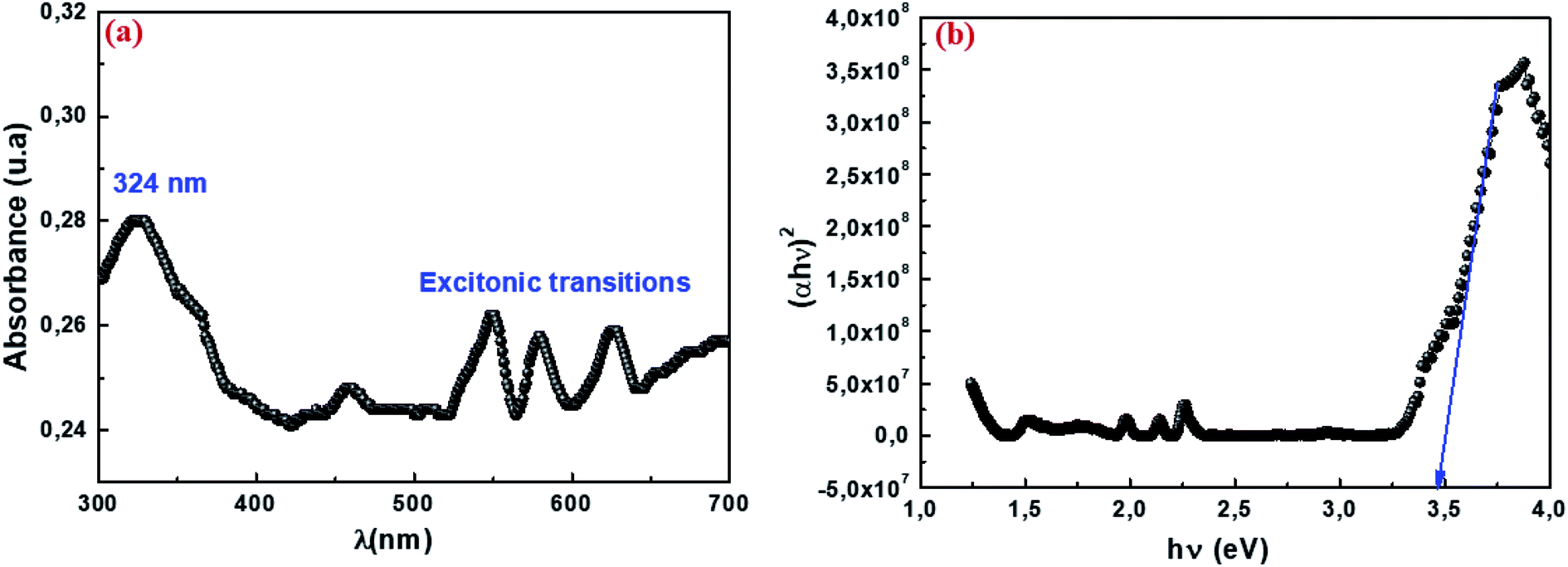
The absorption spectrum of our sample is shown in Fig. 6a in a measurement range extending from ultraviolet (UV) to visible (VIS), or wavelengths ranging from 300 to 700 nm. The spectrum shows an absorption band that has a maximum in the UV range. The intense band observed around 324 nm indicates the gap of the material, while the other bands are attributed to the excitonic transition. Previous studies have shown that absorption can be attributed to the photoexcitation of electrons from the valence band to the conduction band (ligand-to-metal (p–d) type charge transition O2p ⇨ Mn3d).58 The optical band gap (Eg) is the main characteristic of materials that are considered good candidates for optoelectronic applications. The energy of the forbidden band Eg of our sample was determined using the following formula Eg = hc/λ. The value of Eg is 3.82 eV. The optical gap value was then determined according to the Tauc model:59where α is the absorption coefficient, hυ is the energy of the incident radiation expressed in eV, A is a constant reflection of the amorphous solid structure's disorder degree, Eg is the gap energy and the exponent n characterizes the type of optical transition. Accordingly, it has four values 1/2, 2 and 1/3, 3 for direct, indirect allowed transition and direct and indirect forbidden transition respectively. Most semiconductors exhibit an allowed direct transition mechanism. Fig. 6b presents the curve (αhν)2 as a function of hν. The gap energy was deduced from the intersection of the linear part with the energy axis. It is equal to 3.46 eV. This result indicates that our material could be a promising candidate for certain applications such as photodetectors, photovoltaics, and photocatalysts. This would be possible through collecting more photons of light to excite the electrons from the valence band to the conduction band.60
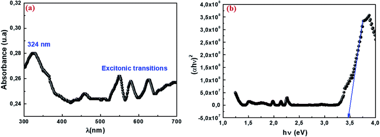 |
| | Fig. 6 UV-visible absorption spectrum at room temperature (a) and variation in (αhν)2 vs. the energy of the photon hν (b) for nanoparticles Cu1.5Mn1.5O4. | |
3.5. Electrical results
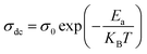
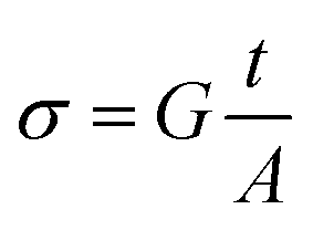
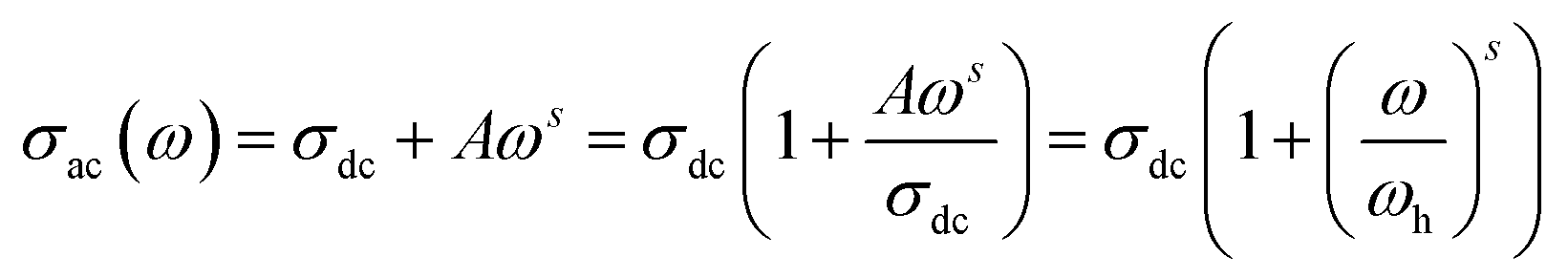
3.5.1. Conductivity studies. The electrical conductivity of Cu1.5Mn1.5O4 nanoparticles was calculated from the relation:| |
 | (14) |
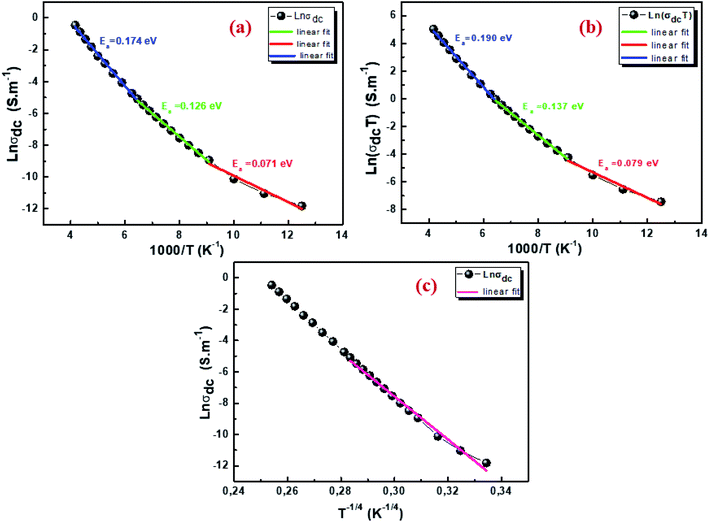
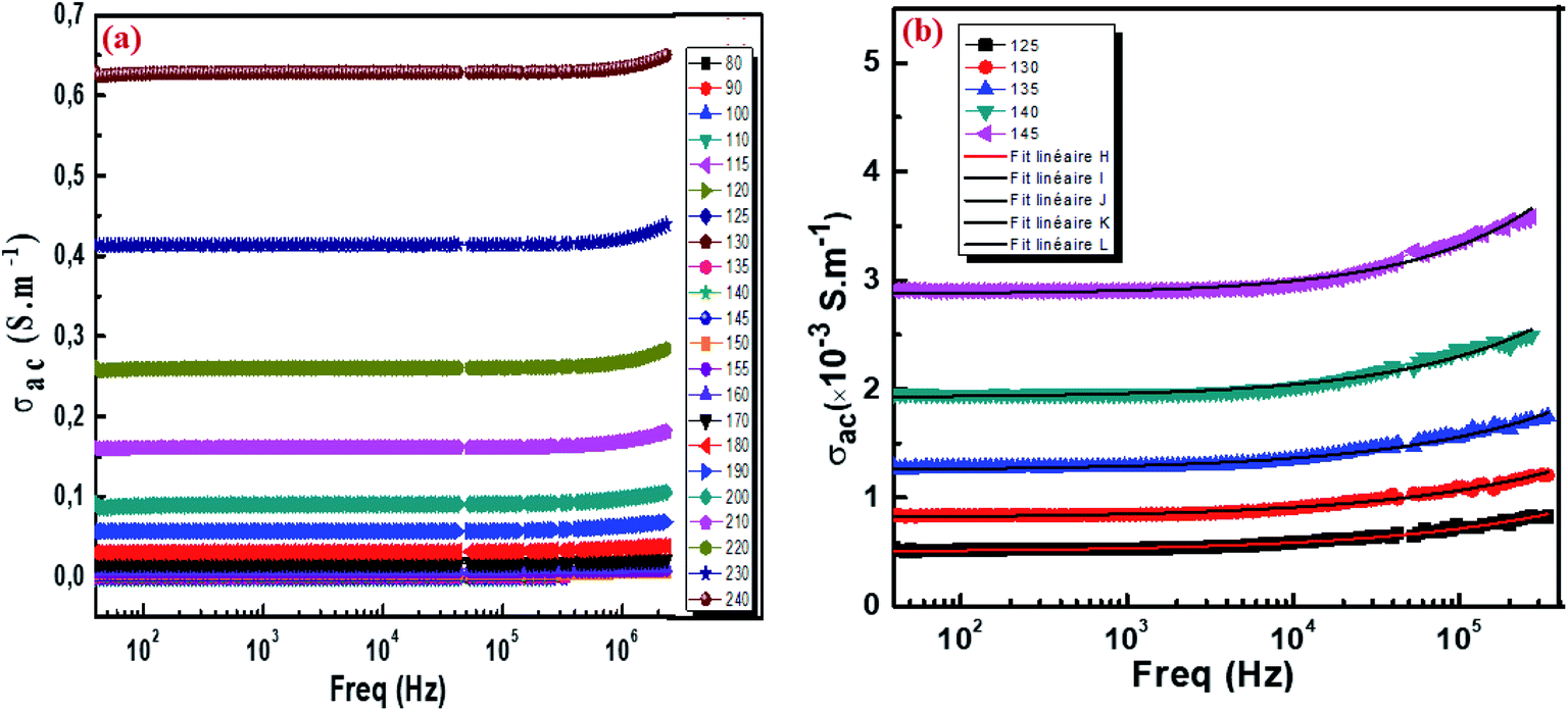
where G is the electrical conductance, t is the thickness and A is the area of cross-section of the pellet. Fig. 7a shows that the conductivity σ increases as we increase the temperature, which indicates the thermal activation of the conduction process in Cu1.5Mn1.5O4 nanoparticles. The conductivity σ presents two different types of behavior as a function of frequency:61,62 (i) at low frequencies, the conductivity σ is constant for a given temperature in a frequency range up to about 104 Hz (Fig. 7b), which represents a uniform behavior attributed to the direct current conductivity (σdc). (ii) At high frequencies we observe an increase in conductivity, which may make available more carriers' loads that come into play and more mechanism for jumping charge carriers between successive sites in this material. This then represents a dispersive behavior, being the alternative current conductivity (σac). The electrical conductivity follows Jonscher's law:63where σdc is the direct current conductivity, A is a temperature-dependent constant, and ω is the angular frequency ω = 2πf. The exponent s is a dimensionless parameter that reflects the interaction degree between the mobile charge carriers and their environments. It has been used frequently to characterize electrical conduction in glasses, amorphous semiconductors, ionic conductors and some crystals.64 Using eqn (15), we made a fit of the curves shown in Fig. 7a for the temperatures (T = 125 K, 130 K, 135 K, 140 K, and 145 K) and Fig. 7b to deduce the values of σdc, A and the exponent s. The origin of Jonscher's dependence of conductivity as a function of temperature may be attributed to the relaxation of the ionic atmosphere following the movement of the particles.65 To understand the relaxation process, we analyzed the conductivity response σdc with the temperature according to the following three models. Fig. 8a shows the logarithmic variation of the conductivity σdc as a function of the inverse of the temperature in the range from 80 to 240 K. The curve has a linear behavior in three regions, which confirms the thermal activation (TA) of the conduction process in Cu1.5Mn1.5O4 nanoparticles. The activation energies for the electrical conductivity were obtained from the Arrhenius relation:66| |
 | (16) |
where σ0 is a pre-exponential factor, Ea is the activation energy, KB is the Boltzmann constant (KB = 8.625 × 10⁻⁵ eV K−1) and T is the absolute temperature. The experimental data of dc conductivity are well fitted by the Mott and Davis law,67 which describes small polaron hopping (SPH):| |
 | (17) |
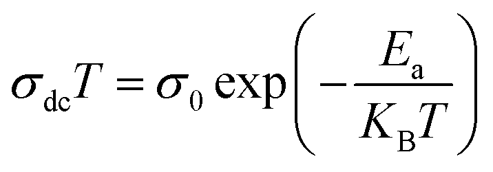
where σ0 is a pre-exponential factor, Ea is the activation energy, KB is the Boltzmann constant and T is the absolute temperature. The plot of ln(σdc × T) vs. (1000/T) shown in Fig. 8b for Cu1.5Mn1.5O4 nanoparticles shows an increase in the conductivity with the temperature, confirming that the conduction process is thermally activated. This result is expected of spinel semiconductor behavior.68,69 The Ea values are estimated from the slope of the linear fit plot. The fit results in the σ–T curves clearly indicate that both models: TA thermal activation and small polaron hopping (SPH) are responsible for the conduction mechanism and predominance at high temperatures. The activation energies for TA and SPH models are collated in Table 2.
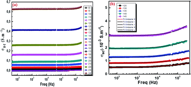 |
| | Fig. 7 The frequency variation of the conductivity at different temperatures of Cu1.5Mn1.5O4 nanoparticles (a) and fit of the curves for some representative temperature (b). | |
 |
| | Fig. 8 Arrhenius plot of electrical conductivity with 1000/T (a), plot of ln(σdcT) with 1000/T (b), and plot of ln(σdc) with T−1/4 for Cu1.5Mn1.5O4 nanoparticles (c). | |
Table 2 Activation energy obtained from the TA and SPH model of Cu1.5Mn1.5O4 nanoparticles
| TA |
SPH |
| R1 |
R2 |
R3 |
R1 |
R2 |
R3 |
| [80–110 K] |
[110–155 K] |
[155–240 K] |
[80–110 K] |
[110–155 K] |
[155–240 K] |
| Ea = 0.071 eV, ±0.009 |
Ea = 0.126 eV, ± 0.002 |
Ea = 0.174 eV, ± 0.003 |
Ea = 0.079 eV, ± 0.009 |
Ea = 0.137 eV, ± 0.002 |
Ea = 0.190 eV, ± 0.003 |
The variable range hopping (VRH) conduction model explains the nature of the nanocrystalline grain boundary diffusion mechanism:
| | |
σdc = σ0exp(T0/T)0.25
| (18) |
where
σ0 is a pre-exponential factor,
T is the absolute temperature and
T0 is the temperature of Mott, and its value was calculated from the slope of the curve ln(
σdc) as a function of (
T)
−0.25. According to
Fig. 8c, the variation in ln(
σdc) with T
−1/4 obeys the variable range hopping conduction mechanism. Consequently, we deduce that the transport model (VRH) can be a predominantly low-temperature transport process. Such behavior has been observed in semiconductor oxides and perovskites,
70,71 where a change in the conduction mechanism at low temperatures is generally observed. The temperature of Mott (
T0) deduced from
Fig. 8c is 3.575 × 10
8 K.
67| |
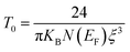 | (19) |
where
ξ represents the decay length of the localized wave function,
KB is the Boltzmann constant and
N(
EF) is the density of states at the Fermi level. Based on
eqn (19), it was found that the value of
T0 will be higher as the energy states' number at the Fermi level decreases,
N(
EF) = 9.18 × 10
20 eV
−1 cm
−3.
In order to understand the conduction mechanisms in our dielectric materials, four models have been proposed. These models are based on tunneling load transport mechanisms by jumping over a potential barrier or through this barrier:
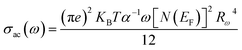
The quantum mechanical tunneling (QMT) model: according to the (QMT) model,72 the exponent s is almost equal to 0.8 and slightly increases with or without temperature. The conductivity σac is given by the relation:
| | |
σac(ω) = Ce2aKBT[N(EF)]2ωRω4
| (20) |
where
C is a constant,
e is the charge of electron,
a is the localized ray,
T is the absolute temperature,
N(
EF) is the state density at the Fermi level,
KB is the Boltzmann constant,
ω is the angular frequency and
Rω is the hop length at the frequency:
| |
 | (21) |
The exponent s can be calculated using the following formula:
| |
 | (22) |
where
α is the inverse localization length,
ω is the angular frequency and
τ0 is the relaxation time.
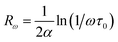
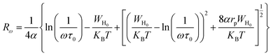
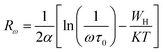
For the correlated barrier hopping (CBH) model,73 the parameter s decreases as the temperature increases. It is as follows:
| |
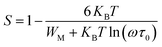 | (23) |
where
KB is the Boltzmann constant,
T is the absolute temperature,
WM is the maximum value of the height of the potential barrier, also called ionization energy,
ω is the angular frequency and
τ0 denotes the characteristic relaxation time of the order of the atomic vibrational period (
τ0 = 10
−12 s). For fairly high values of
WM/
KBT,
eqn (23) becomes
| |
 | (24) |
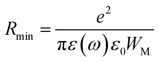
From this equation, we can calculate the maximum value of the potential barrier's height WM, which is connected to the distance Rmin of the jump between the two neighboring wells according to eqn (25):74
| |
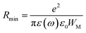 | (25) |
where
e is the electronic charge,
ε(
ω) is the permittivity of the material,
ε0 is the dielectric permittivity of the vacuum and
WM is the maximum value of the height of the potential barrier, also called ionization energy.
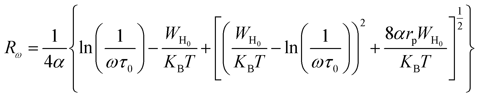
For the overlapping large polaron tunneling (OLPT) model,75 the conductivity is given by the following expression:
| |
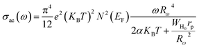 | (26) |
where
e is the electronic charge,
KB is the Boltzmann constant,
T is the absolute temperature,
N(
EF) is the states' density at the Fermi level,
rp is the radius of the large polaron,
α is the inverse localization length,
WH0 is the activation energy associated with the transfer load between the overlapping sites, and
Rω is the jump length at the angular frequency
ω (which is the tunneling distance).
The jump length Rω was determined using the following equation:
| |
 | (27) |
where
α is the inverse localization length,
ω is the angular frequency,
τ0 is the characteristic relaxation time,
WH0 is the activation energy associated with the transfer load between the overlapping sites,
KB is the Boltzmann constant,
T is the absolute temperature and
rp is the radius of the large polaron.
According to this model, the exponent s is expressed by the following relation:
| |
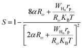 | (28) |
where
α is the inverse localization length,
Rω is the jump length at the angular frequency
ω (which is the tunneling distance),
WH0 is the activation energy associated with the transfer load between the overlapping sites,
rp is the radius of the large polaron,
KB is the Boltzmann constant and
T is the absolute temperature.
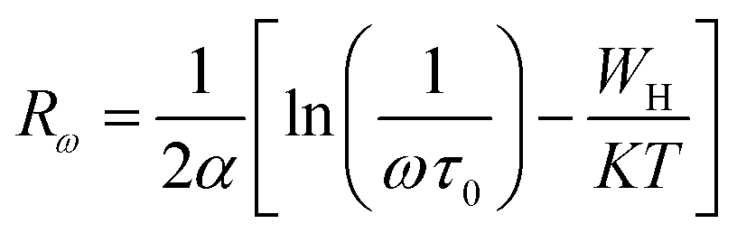
In the non-overlapping small polaron tunneling (NSPT) model, the exponent s increases as the temperature increases and varies according to the following formula:63
| |
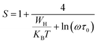 | (29) |
with
τ0 is the relaxation time associated with the polaron formation process,
ω is the angular frequency,
WH is the activation energy of the polarons,
KB is the Boltzmann constant and
T is the absolute temperature.
AC conductivity σac is written as follows:
| |
 | (30) |
with
| |
 | (31) |
where
Rω is the tunnel distance,
e is the electronic charge,
KB is the Boltzmann constant,
T is the absolute temperature,
α−1 is the spatial extension of the polaron,
ω is the angular frequency,
N(
EF) is the density of states near the Fermi level,
τ0 is the relaxation time associated with the polaron formation process and
WH is the activation energy of the polarons.
Fig. 9 reflects the exponent's variation as a function of temperature. This exponent decreases as the temperature increases predicting a minimum value and then increases as the temperature increases. Such behavior is consistent with the OLPT model. The latter is considered the appropriate model to explain the electrical conduction mechanism in our compound throughout the temperature range. Our result is in agreement with the previous report of Yan et al.76 The σ–T curves in Fig. 8a and b show the existence of three regions for different temperature ranges, which implies that each region is characterized by a conduction mechanism. The exponent's variation (s) as a function of the temperature in Fig. 9 shows that in the region (I) [80–110 K], s decreases as the temperature increases and the mechanism (CBH) is predominant.77 In region (II) [110–155 K], the exponent also decreases as the temperature increases to a minimum value at a certain temperature, then increases as the temperature increases. The appropriate conduction mechanism is the multilayer tunneling effect (OLPT).75 In the region (III) [155–240 K], the exponent s increases as the temperature increases. The appropriate model for characterizing the electrical conduction in this region is the small polar tuning (NSPT) without overlap.78
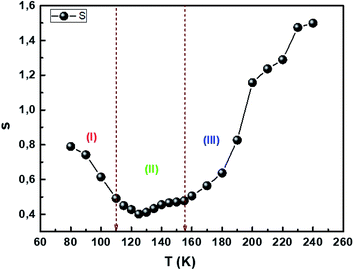 |
| | Fig. 9 Temperature evolution of the s parameter. | |
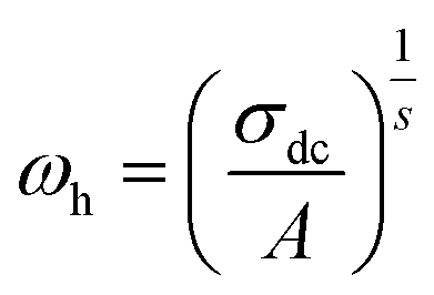
The power law is determined from Jonscher's equation using the Almond–West expression:79
| |
 | (32) |
where
σdc is the direct current conductivity,
A is a temperature-dependent constant, and
ω is the angular frequency
ω = 2π
f. The exponent
s is a dimensionless parameter that reflects the interaction degree between the mobile charge carriers and their environments.
| |
 | (33) |
where
ωh is the crossover frequency from dc to dispersive conductivity region at
ω >
ωh, it is known as the hopping frequency of the charge carrier.
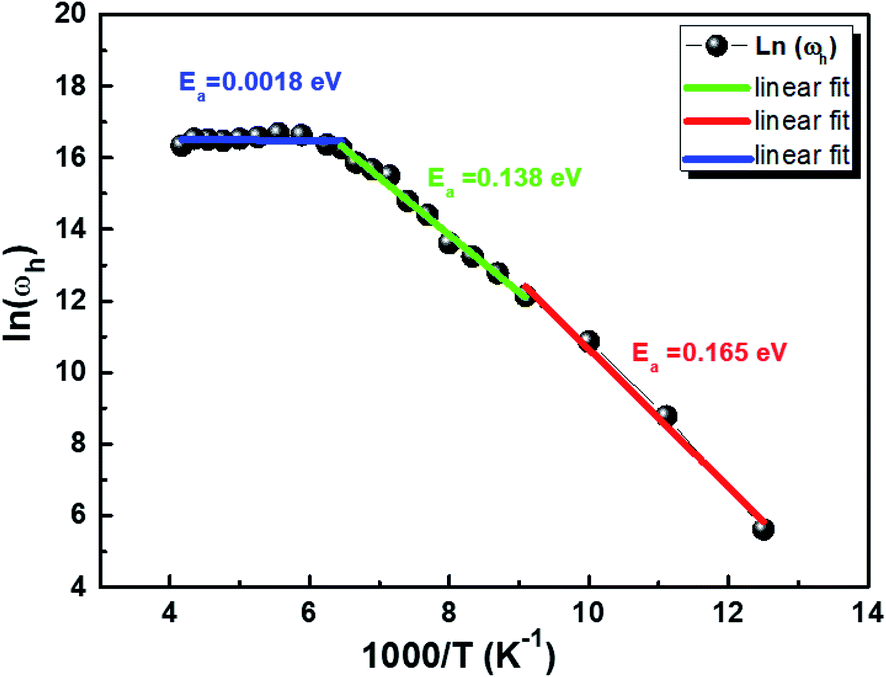
Fig. 10 displays the plot of ln (ωh) as a function of (1000/T) corresponding to the conduction of grain for Cu1.5Mn1.5O4 in which the activation energy for the second region in Table 3 is nearly similar to that found previously from the DC conductivity of grains. We can therefore conclude that the mobility of charge carriers in this material is provided by the simple hopping mechanism at this region.79
 |
| | Fig. 10 Variation of ln(ωh) as a function of (1000/T). | |
Table 3 Activation energy obtained from the hopping frequency (ωh) of Cu1.5Mn1.5O4 nanoparticles
| R1 |
R2 |
R3 |
| [80–110 K] |
[110–155 K] |
[155–240 K] |
| Ea = 0.165 eV, ± 0.011 |
Ea = 0.138 eV, ± 0.004 |
Ea = 0.0018 eV, ± 0.004 |
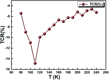
The temperature coefficient of resistivity (TCR) is important for sensor material performance used in an uncooled IR bolometer, as defined by the equation:20
| | |
TCR = [(1/ρ) × (dρ/dT)] × 100%
| (34) |
where
ρ = 1/
σdc is the resistivity. We checked out whether our compound can be useful for these applications. We plotted in
Fig. 11 the temperature-dependent temperature coefficient of resistivity for our sample and determined the TCR factor. The Cu
1.5Mn
1.5O
4 compound shows that a high negative TCR value is equal to −15% K
−1. Compared to other values of TCR collected from other works,
80,81 our Cu
1.5Mn
1.5O
4 sample has a higher TCR value. The present result may act as a potential candidate for infrared detectors and uncooled infrared bolometric applications.
 |
| | Fig. 11 The variation of TCR % as a function of temperature of Cu1.5Mn1.5O4 nanoparticles. | |
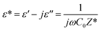
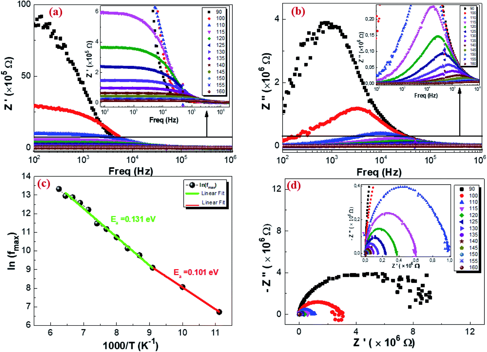
3.5.2. Complex impedance results. The complex impedance of dielectric material is presented as follows:where Z′ and Z′′ are the real part and the imaginary part of the complex impedance, respectively. Fig. 12a and b show the variation in the real Z′ and imaginary Z′′ part as a function of frequency in the temperature range from 90 K to 160 K. We can notice that, in the lower frequency limit, Z′ is almost constant, and then, it decreases as the frequency and temperature increase. This result indicates a thermal activation behavior (Fig. 12a). In addition, the increasing trend of Z′, at the lower frequency limit, with the decrease in temperature is explained by the decrease in the AC conductivity due to the increase of the charge carrier mobility and a decrease in the density of trapped charges.82 At a higher frequency, Z′ decreases rapidly and converges to a constant value. This can be explained by the increase in the AC conductivity in this range due to the release of immobile charges and the decrease in the trapped charges' density.65 Furthermore, as illustrated in Fig. 12b, the spectrum of Z′′ reaches a maximum reflecting the presence of relaxation frequencies corresponding to the grains.83 Here, the peak gradually shifts towards higher frequencies when the temperature increases, indicating a thermal activated relaxation process. In order to estimate the activation energy of the contributions of the Cu1.5Mn1.5O4 compound, we have plotted in Fig. 12c the variation in Ln(fmax) vs. 1000/T, where fmax is the frequency at which the maximum of Z′′ occurs; the obtained curve obeys the following Arrhenius law:| |
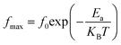 | (36) |
where f0 is a pre-exponential factor, Ea the activation energy, KB = 8.625 × 10⁻⁵ eV K−1 is the Boltzmann constant, and T is the measurement temperature. The obtained values of the activation energy are 0.101 eV for R1 and 0.131 eV for R2. It is worth noting that the activation energy value corresponds to the second region R2 and is close to those obtained by DC analysis. This suggests that during conduction and relaxation processes, the charge carriers need to overcome approximately the same energy barrier.
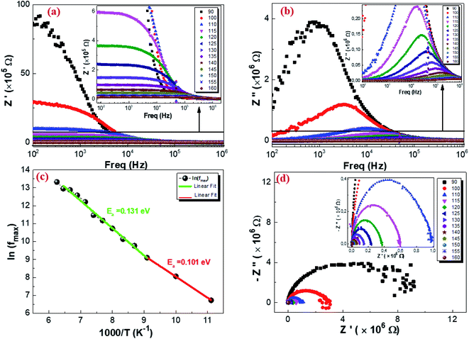 |
| | Fig. 12 Real part (a), imaginary part of the impedance plot as a function of frequency at different temperatures (b), variation of ln(fmax) vs. 1000/T from the impedance data (c), and Nyquist plot of Cu1.5Mn1.5O4 nanoparticles (d). | |
Fig. 12d represents the complex impedance plots of Z′′ versus Z′ of Cu1.5Mn1.5O4 at different temperatures, which is generally known as a Nyquist plot to distinguish the contributions of grains, grain boundaries and electrodes.84 The impedance spectra are constituted by semicircular arcs, which their radius of curvature decreases as a result of the increase in temperature. This behavior indicates a thermally activated conduction mechanism.85 The appearance of this semicircular arc is associated with the grain effect.
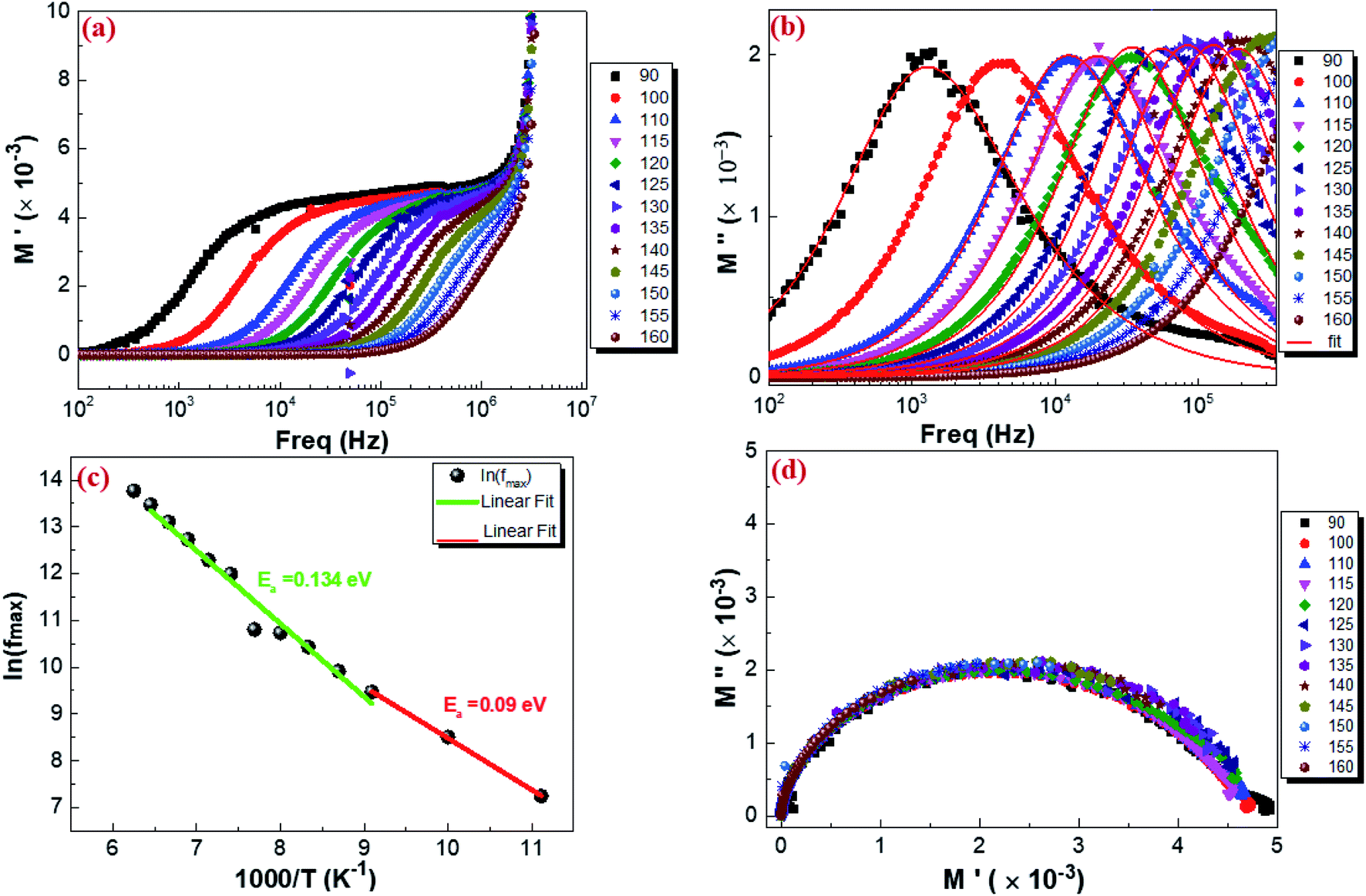
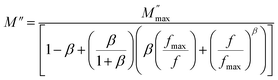
3.5.3. Complex modulus analysis. The electrical aspects of our compound can be described using the complex electric modulus M* given by:86| | |
M* = M′ + iM′′ = iω0C0Z*
| (37) |
where M′ is the real part and M′′ is the imaginary part of the complex modulus and C0 is the vacuum capacitance of the cell under investigation. Fig. 13 shows a typical frequency dependence of the real part of the complex electrical modulus M′ (a), the imaginary part of the complex electrical modulus M′′ (b) and the Argand plot (M′′vs. M′) (d) of Cu1.5Mn1.5O4 with the increase in frequency in the temperature range from 90 K to 160 K. It is observed in Fig. 13a that real modulus M′ plots exhibit a value of M′ that approaches zero for all temperatures at low frequency. This proves that the electrode polarization effect is excluded. The frequency increase indicates the existence of dispersion and then shows a plateau at higher frequencies. It is seen from Fig. 13b that the modulus spectra M′′ have a single electrical relaxation peak for all temperatures, which is associated with the grain effect, centered at the dispersion region of M′.87,88 This relaxation peak moves toward higher frequencies associated with the increase in temperature. Thus, it can be concluded that the relaxation process is temperature dependent.89 At the low-frequency region meaning at frequencies below the maximum peak  there is a pure conduction process90 where the charge carriers drift to long distances. However, at the high-frequency region it is at frequencies above the maximum peak
  the carriers are spatially constrained to move freely only within their potential wells over short distances.91 The M′′(f) experimental data have been adjusted according to the Bergman proposed Kohlrausch, Williams and Watts (KWW) function:92
| |
 | (38) |
where  is the peak maxima, fmax is its corresponding frequency and β is the stretching factor (0 < β < 1), which indicates a Debye or non-Debye type of the dielectric relaxation.93 As per eqn (38), the parameters obtained from the fitted data of M′′(f) at different temperatures for our compound are collated in Table 4. We thus notice that all values of β are less than unity. This confirms the non-Debye behavior for the Cu1.5Mn1.5O4 compound. We plotted in Fig. 13c the variation in Ln(fmax) vs. 1000/T, where fmax is the frequency at which the maximum of M′′ occurs in order to estimate the activation energy of the contributions for the Cu1.5Mn1.5O4 compound. The obtained curve obeys the Arrhenius law. The obtained values of the activation energy revealed that R1 is 0.09 eV and R2 is 0.134 eV. It was found that our results confirm those obtained from the imaginary part of the impedance Z′′ and justify the goodness of both adjustments of M′′ vs. frequency and Nyquist curves. Fig. 13d shows the Argand plot for electric modulus (M′′ vs. M′) at different temperatures of the Cu1.5Mn1.5O4 sample. We observe a single semicircle associated with the grain effect. When the temperature increases, this semicircle transforms from a closed semicircle to an arc. Here, in the M′′ vs. M′ plot, the existence of non-semicircles indicates non-Debye-type relaxation.
 |
| | Fig. 13 Real part (a), imaginary part of the electrical modulus plot as a function of frequency at different temperatures (b), variation of ln(fmax) vs. 1000/T from the modulus data (c), and Argand plot of Cu1.5Mn1.5O4 (d). | |
Table 4 Theoretical parameters obtained from the fitted data of the imaginary part of modulus as a function of frequency at different temperatures of Cu1.5Mn1.5O4
| T (K) |

(10−3) |
β |
fmax (Hz) |
| 90 |
2.02 |
0.774(5) |
1404 |
| 100 |
1.95 |
0.797(9) |
4953 |
| 110 |
1.97 |
0.876(7) |
12980 |
| 115 |
2.05 |
0.923(1) |
20260 |
| 120 |
1.98 |
0.920(9) |
34040 |
| 125 |
2.30 |
0.968(7) |
45790 |
| 130 |
2.57 |
0.971(8) |
49310 |
| 135 |
2.11 |
0.976(7) |
161500 |
| 140 |
2.08 |
0.853(6) |
217200 |
3.6. Dielectric study
The dielectric response of a semiconductor material can be defined by the following equation:94| |
 | (39) |
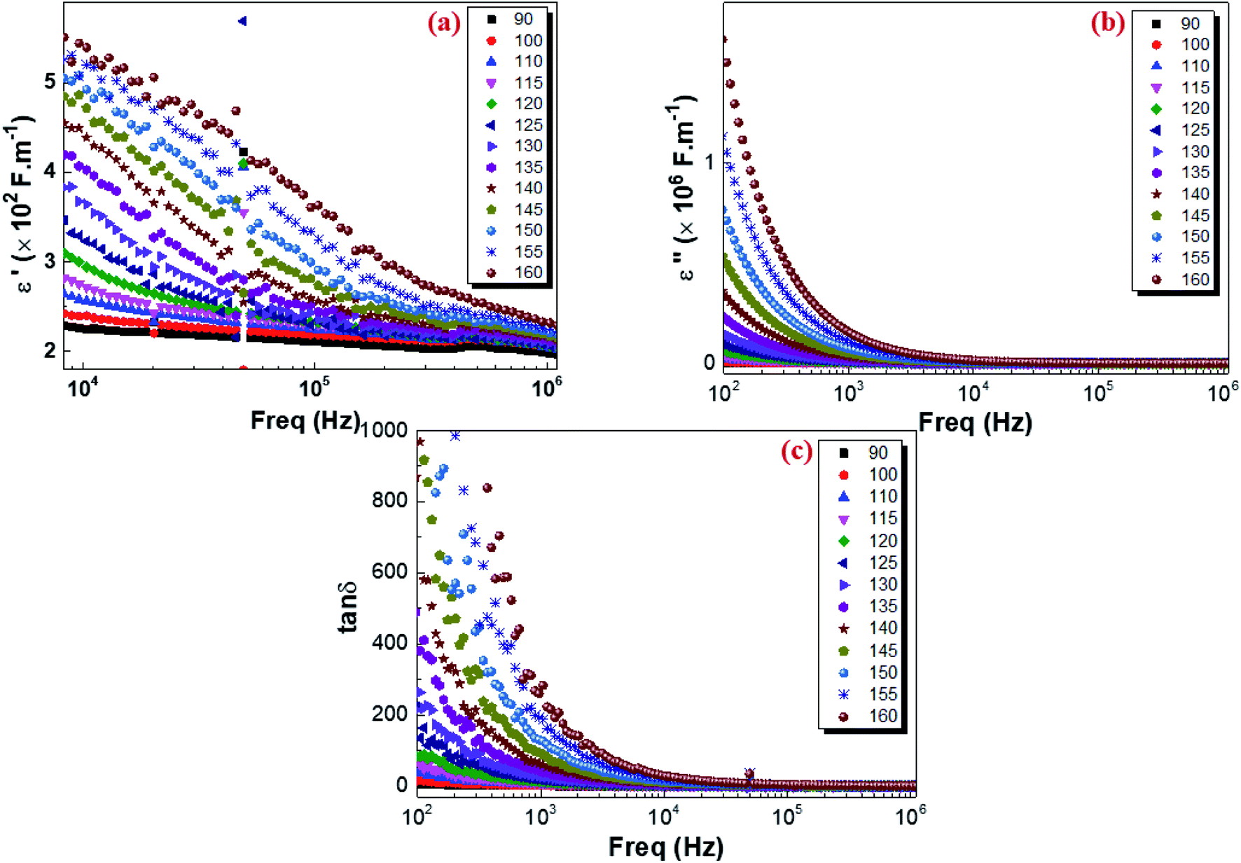
where C0 is the vacuum capacitance of the capacitor and the terms ε′(ω) and ε′′(ω) the real and the imaginary parts of the dielectric permittivity describing respectively the storage and the loss of energy in the material. The isothermal frequency-dependent real part of the complex dielectric permittivity (ε′), imaginary part of the relative dielectric constant (ε′′) and dielectric loss of the Cu1.5Mn1.5O4 are shown in Fig. 14a, b and c respectively. It was found that the dielectric constant increases as the temperature increases, while ε′ and ε′′ follow an inverse frequency dependence. At low frequencies, high dielectric values can be explained by the increase in the polarization in the structure caused by the charge carriers' high mobility and associated with the increase in the temperature. ε′ and ε′′ decrease as the frequency increases and remain constant at higher frequencies. This is attributed to the orientation of the electric dipoles in the direction of the applied electric field. By increasing the frequency, all mechanisms of polarization cannot follow the orientation of the applied electric field. Consequently, the reorientational motion of the charge carriers tends to decrease the real part of permittivity ε′ values. This behavior is similar to that observed for other amorphous semiconductors.95 The tangent loss (tanδ) presents the dissipation of energy in dielectric system that is proportional to the imaginary part of permittivity.96 According to Fig. 14c, we note that at low frequencies, the losses are high and they gradually decrease at high frequencies until reaching a lower saturated value. As shown in Fig. 7, electrons can require more energy for conduction through grains, which can be due to the lower conductivity at lower frequencies. Thus, the energy dissipation is high showing in greater tangent losses. Whereas, at high frequency, the losses are reduced and the dipoles contribute to the polarization because the dipole polarization can orient themselves with the electric field, due to high conductivity.97 Finally, these results indicate that the Cu1.5Mn1.5O4 nanoparticle sample could be used in many technological applications, e.g., Li-ion batteries, fuel cells, microwaves, and low-temperature cofired ceramics (LTCC) technology applications.
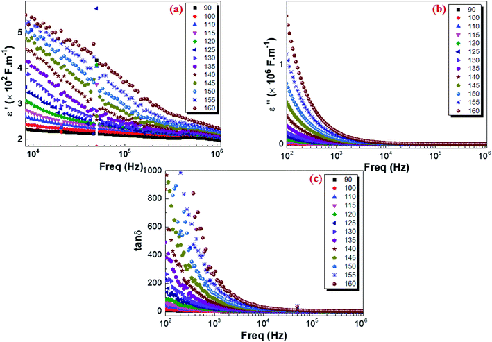 |
| | Fig. 14 Variation in the real part of the dielectric constant ε′(a), imaginary part of the dielectric constant ε′′(b), and the dielectric loss tanδ (c) with the frequency at various temperatures for Cu1.5Mn1.5O4 nanoparticles. | |
4. Conclusion
The structural, optical, electrical and dielectric properties of the cubic spinel Cu1.5Mn1.5O4 prepared via a sol–gel route have been investigated. The XRD measurements showed that our compound crystallizes in the Fdm cubic structure with a nanometer grain size and presents a CuO minority phase. The study by FTIR and Raman spectroscopy confirms the formation of our spinel compound. The optical band gap, determined by absorption spectrum, was evaluated at 3.82 eV, which presents a semiconductor behavior that will be more suitable for certain applications such as photodetectors, optoelectronics, photovoltaics and gas sensors. Additionally, the electrical conductivity measurements comply with Jonscher's law. The transportation of charge carriers follows two mechanisms: the nearest neighbor hopping, which transforms to Mott's variable-range-hopping when the temperature decreased. The variation in the exponent s as a function of temperature proves that the CBH model is associated with the conduction mechanism in region (I) and the (OLPT) model in region (II), while in region (III), the suitable model is NSPT. Electric modulus and impedance results have been shown one contribution of grain to the relaxation mechanism. This relaxation shifts to higher frequencies when the temperature increases. The activation energy was determined from the AC conduction, the imaginary part of impedance (Z′′) and the modulus (M′′). This suggests that during conduction and relaxation processes, the charge carriers need to overcome approximately the same energy barrier. Dielectric results present a high dielectric permittivity that proves to be useful in different technological applications.
Conflicts of interest
There are no conflicts to declare.
Acknowledgements
The authors acknowledge the support of the Tunisian Ministry of Higher Education and Scientific Research within the framework of the Tunisian-Portuguese cooperation in the field of scientific research and technology. CFisUC is supported by national funds from FCT – Fundação para a Ciência e a Tecnologia, I.P., within the project UID/04564/2020. Access to TAIL-UC facility funded under QREN-Mais Centro Project No ICT_2009_02_012_1890 is gratefully acknowledged.
Notes and references
- J. Ignaczak, Y. Naumovich, K. Górnicka, J. Jamroz, W. Wróbel, J. Karczewski, M. Chen, P. Jasiński and S. Molin, J. Eur. Ceram. Soc., 2020, 40, 5920–5929 CrossRef CAS.
- K. M. Batoo and M.-S. A. El-sadek, J. Alloys Compd., 2013, 566, 112–119 CrossRef CAS.
- A. Hilczer, K. Kowalska, E. Markiewicz, A. Pietraszko and B. Andrzejewski, Mater. Sci. Eng., B, 2016, 207, 47–55 CrossRef CAS.
- A. S. Albuquerque, M. V. C. Tolentino, J. D. Ardisson, F. C. C. Moura, R. de Mendonça and W. A. A. Macedo, Ceram. Int., 2012, 38, 2225–2231 CrossRef CAS.
- R. Ali, A. Mahmood, M. A. Khan, A. H. Chughtai, M. Shahid, I. Shakir and M. F. Warsi, J. Alloys Compd., 2014, 584, 363–368 CrossRef CAS.
- P. Priyadharsini, A. Pradeep, P. S. Rao and G. Chandrasekaran, Mater. Chem. Phys., 2009, 116, 207–213 CrossRef CAS.
- H. Yang, X. Zhang, W. Ao and G. Qiu, Mater. Res. Bull., 2004, 39, 833–837 CrossRef CAS.
- M. Penchal Reddy, W. Madhuri, G. Balakrishnaiah, N. Ramamanohar Reddy, K. V. Siva Kumar, V. R. K. Murthy and R. Ramakrishna Reddy, Curr. Appl. Phys., 2011, 11, 191–198 CrossRef.
- P. Pulišová, J. Kováč, A. Voigt and P. Raschman, J. Magn. Magn. Mater., 2013, 341, 93–99 CrossRef.
- M. Bobruk, K. Durczak, J. Dąbek and T. Brylewski, J. Mater. Eng. Perform., 2017, 26, 1598–1604 CrossRef CAS.
- J. Quan, L. Mei, Z. Ma, J. Huang and D. Li, RSC Adv., 2016, 6, 55786–55791 RSC.
- X.-D. Zhang, Z.-S. Wu, J. Zang, D. Li and Z.-D. Zhang, J. Phys. Chem. Solids, 2007, 68, 1583–1590 CrossRef CAS.
- M. Zhao, J. Huang, Y. Zhou, Q. Chen, X. Pan, H. He and Z. Ye, Biosens. Bioelectron., 2013, 43, 226–230 CrossRef CAS.
- S. Wijewardane and D. Y. Goswami, Renew. Sustain. Energy Rev., 2012, 16, 1863–1873 CrossRef CAS.
- Q.-F. Geng, X. Zhao, X.-H. Gao and G. Liu, J. Am. Ceram. Soc., 2011, 94, 827–832 CrossRef CAS.
- A. Reddy, C. Gopinath and S. Chilukuri, J. Catal., 2006, 243, 278–291 CrossRef CAS.
- H. Zhao, X. X. Zhou, L. Y. Pan, M. Wang, H. R. Chen and J. L. Shi, RSC Adv., 2017, 7, 20451–20459 RSC.
- F. Li, R. Zhang, Q. Li and S. Zhao, Res. Chem. Intermed., 2017, 43, 6505–6519 CrossRef CAS.
- P. Ma, Q. Geng, X. Gao, S. Yang and G. Liu, RSC Adv., 2016, 6, 32947–32955 RSC.
- M. D. Daivajna, A. Rao and G. S. Okram, J. Magn. Magn. Mater., 2015, 388, 90–95 CrossRef CAS.
- S. Chen, H. Ma, S. Wang, N. Shen, J. Xiao, H. Zhou, X. Zhao, Y. Li and X. Yi, Thin Solid Films, 2006, 497, 267–269 CrossRef CAS.
- X.-M. Liu, H.-J. Fang and L.-T. Liu, Microelectron. J., 2007, 38, 735–739 CrossRef CAS.
- F. Yang, L. Mechin, J. M. Routoure, B. Guillet and R. Chakalov, J. Appl. Phys., 2006, 99, 024903 CrossRef.
- Y. Hou, Z. Huang, Y. Gao, Y. Ge, J. Wu and J. Chu, Appl. Phys. Lett., 2008, 92, 202115 CrossRef.
- S. Karanth, M. A. Sumesh, V. Shobha, H. G. Shanbhogue and C. L. Nagendra, Sens. Actuators Phys., 2009, 153, 69–75 CrossRef CAS.
- H. Schmidt, J. Sol-Gel Sci. Technol., 2006, 40, 115–130 CrossRef CAS.
- H. M. Rietveld, J. Appl. Crystallogr., 1969, 2, 65–71 CrossRef CAS.
- D. K. Smith, J. Fiala and E. Ryba, Powder Diffr., 1993, 8, 252–254 CrossRef.
- V. A. M. Brabers and R. E. Vandenberghe, Phys. Lett. A, 1973, 44, 493–494 CrossRef CAS.
- K. Momma and F. Izumi, J. Appl. Crystallogr., 2011, 44, 1272–1276 CrossRef CAS.
- R. E. Vandenberghe, G. G. Robbrecht and V. A. M. Brabers, Mater. Res. Bull., 1973, 8, 571–579 CrossRef CAS.
- R. J. Hill, J. R. Craig and G. V. Gibbs, Phys. Chem. Miner., 1979, 4, 317–339 CrossRef CAS.
- S. Nasrin, S. M. Hoque, F. U. Z. Chowdhury and M. M. Hossen, J. Appl. Phys., 2014, 6, 58–65 Search PubMed.
- A. V. Humbe, A. C. Nawle, A. B. Shinde and K. M. Jadhav, J. Alloys Compd., 2017, 691, 343–354 CrossRef CAS.
- S. G. Kakade, R. C. Kambale, C. V. Ramanna and Y. D. Kolekar, RSC Adv., 2016, 6, 33308–33317 RSC.
- M. George, A. Mary John, S. S. Nair, P. A. Joy and M. R. Anantharaman, J. Magn. Magn. Mater., 2006, 302, 190–195 CrossRef CAS.
- L. Aswaghosh, D. Manoharan and N. V. Jaya, Phys. Chem. Chem. Phys., 2016, 18, 5995–6004 RSC.
- E. R. Kumar, Ch. Srinivas, M. S. Seehra, M. Deepty, I. Pradeep, A. S. Kamzin, M. V. K. Mehar and N. K. Mohan, Sens. Actuators Phys., 2018, 279, 10–16 CrossRef CAS.
- A. Guinier, Théorie et technique de la radiocristallographie, Dunod, 1964 Search PubMed.
- L. Motevalizadeh, Z. Heidary and M. E. Abrishami, Bull. Mater. Sci., 2014, 37, 397–405 CrossRef CAS.
- N. S. Gonçalves, J. A. Carvalho, Z. M. Lima and J. M. Sasaki, Mater. Lett., 2012, 72, 36–38 CrossRef.
- J. F. Nye, Physical Properties of Crystals: Their Representation by Tensors and Matrices, Oxford University Press, Oxford Oxfordshire: New York, 1985 Search PubMed.
- Ch. Rayssi, S. E. Kossi, J. Dhahri and K. Khirouni, J. Alloys Compd., 2018, 759, 93–99 CrossRef CAS.
- D. Zákutná, J. Vlček, P. Fitl, K. Nemkovski, D. Honecker, D. Nižňanský and S. Disch, Phys. Rev. B, 2018, 98, 064407 CrossRef.
- S. A. Hosseini, A. Niaei, D. Salari, M. C. Alvarez-Galvan and J. L. G. Fierro, Ceram. Int., 2014, 40, 6157–6163 CrossRef CAS.
- A. F. Costa, P. M. Pimentel, F. M. Aquino, D. M. A. Melo, M. A. F. Melo and I. M. G. Santos, Mater. Lett., 2013, 112, 58–61 CrossRef CAS.
- T. J. Richardson, S. J. Wen, K. A. Strichel, P. N. Ross and E. J. Cairns, Mater. Res. Bull., 1997, 32, 609–618 CrossRef CAS.
- J. Li, Y. Pan, F. Qiu, Y. Wu and J. Guo, Ceram. Int., 2008, 34, 141–149 CrossRef CAS.
- D. Bouokkeze, J. Massoudi, W. Hzez, M. Smari, A. Bougoffa, K. Khirouni, E. Dhahri and L. Bessais, RSC Adv., 2019, 9, 40940–40955 RSC.
- A. Bougoffa, J. Massoudi, M. Smari, E. Dhahri, K. Khirouni and L. Bessais, J. Mater. Sci. Mater. Electron., 2019, 30, 21018–21031 CrossRef CAS.
- J. Massoudi, M. Smari, K. Nouri, E. Dhahri, K. Khirouni, S. Bertaina, L. Bessais and E. K. Hlil, RSC Adv., 2020, 10, 34556–34580 RSC.
- A. Ghasemi and M. Mousavinia, Ceram. Int., 2014, 40, 2825–2834 CrossRef CAS.
- S. R. Naik and A. V. Salker, J. Mater. Chem., 2012, 22, 2740–2750 RSC.
- G. Datt, M. Sen Bishwas, M. Manivel Raja and A. C. Abhyankar, Nanoscale, 2016, 8, 5200–5213 RSC.
- I. H. Campbell and P. M. Fauchet, Solid State Commun., 1986, 58, 739–741 CrossRef CAS.
- X. Yang, W. Tang, Z. Liu, Y. Makita and K. Ooi, J. Mater. Chem., 2002, 12, 489–495 RSC.
- N. Menyuk, K. Dwight and A. Wold, J. Phys., 1964, 25, 528–536 CrossRef CAS.
- N. Mahfoudh, K. Karoui, K. Khirouni and A. Ben Rhaiem, Phys. B Condens. Matter, 2019, 554, 126–136 CrossRef CAS.
- J. Tauc, R. Grigorovici and A. Vancu, Phys. Status Solidi B, 1966, 15, 627–637 CrossRef CAS.
- A. O. Turky, M. Mohamed Rashad, A. E.-H. Taha Kandil and M. Bechelany, Phys. Chem. Chem. Phys., 2015, 17, 12553–12560 RSC.
- N. Chihaoui, M. Bejar, E. Dhahri, M. A. Valente, L. C. Costa and M. P. F. Graça, Int. J. Mater. Eng. Technol., 2015, 13, 129 CrossRef CAS.
- A. R. James, C. Prakash and G. Prasad, J. Phys. Appl. Phys., 2006, 39, 1635–1641 CrossRef CAS.
- N. Chihaoui, R. Dhahri, M. Bejar, E. Dharhi, L. C. Costa and M. P. F. Graça, Solid State Commun., 2011, 151, 1331–1335 CrossRef CAS.
- M. D. INGRAM, Ion. Conduct. Glass, 1987, 28, 215–234 CAS.
- J. R. Macdonald and E. Barsoukov, History, 2005, 1, 1–13 Search PubMed.
- K. P. Padmasree, D. K. Kanchan and A. R. Kulkarni, Solid State Ionics, 2006, 177, 475–482 CrossRef CAS.
- N. Sivakumar, A. Narayanasamy, J.-M. Greneche, R. Murugaraj and Y. S. Lee, J. Alloys Compd., 2010, 504, 395–402 CrossRef CAS.
- N. Sivakumar, A. Narayanasamy, N. Ponpandian, J. M. Greneche, K. Shinoda, B. Jeyadevan and K. Tohji, J. Phys. Appl. Phys., 2006, 39, 4688 CrossRef CAS.
- N. Ponpandian, P. Balaya and A. Narayanasamy, J. Phys. Condens. Matter, 2002, 14, 3221 CrossRef CAS.
- S. Mollah, H. L. Huang, H. D. Yang, S. Pal, S. Taran and B. K. Chaudhuri, J. Magn. Magn. Mater., 2004, 284, 383–394 CrossRef CAS.
- H. Rahmouni, B. Cherif, M. Baazaoui and K. Khirouni, J. Alloys Compd., 2013, 575, 5–9 CrossRef CAS.
- A. Ghosh, Phys. Rev. B: Condens. Matter Mater. Phys., 1990, 41, 1479–1488 CrossRef CAS.
- G. E. Pike, Phys. Rev. B: Solid State, 1972, 6, 1572 CrossRef CAS.
- R. Salam, Phys. Status Solidi A, 1990, 117, 535–540 CrossRef CAS.
- M. Megdiche, C. Perrin-Pellegrino and M. Gargouri, J. Alloys Compd., 2014, 584, 209–215 CrossRef CAS.
- A. R. Long, Adv. Phys., 1982, 31, 553–637 CrossRef CAS.
- E. M. El-Menyawy, I. T. Zedan, A. M. Mansour and H. H. Nawar, J. Alloys Compd., 2014, 611, 50–56 CrossRef CAS.
- S. Nasri, M. Megdiche and M. Gargouri, Ceram. Int., 2016, 42, 943–951 CrossRef CAS.
- D. P. Almond and A. R. West, Solid State Ionics, 1983, 9, 277–282 CrossRef.
- H. Chouaya, M. Smari, I. Walha, E. Dhahri, M. P. F. Graça and M. A. Valente, J. Magn. Magn. Mater., 2018, 451, 344–350 CrossRef CAS.
- C. OuYang, W. Zhou, J. Wu, Y. Gao, F. Zhang and Z. Huang, Sens. Actuators Phys., 2015, 233, 442–450 CrossRef.
- E. Barsoukov and J. R. Macdonald, Impedance Spectroscopy Theory, Experiment, and Applications, 2nd edn, 2005 Search PubMed.
- H. Baaziz, N. K. Maaloul, A. Tozri, H. Rahmouni, S. Mizouri, K. Khirouni and E. Dhahri, Chem. Phys. Lett., 2015, 640, 77–81 CrossRef CAS.
- H. Nyquist, Bell Syst. Tech. J., 1932, 11, 126–147 CrossRef.
- H. Felhi, R. Lahouli, M. Smari, H. Rahmouni, K. Khirouni and E. Dhahri, J. Mol. Struct., 2019, 1179, 1–10 CrossRef CAS.
- R. N. Bhowmik and A. G. Lone, J. Alloys Compd., 2016, 680, 31–42 CrossRef CAS.
- A. Dutta, T. P. Sinha and S. Shannigrahi, Phys. Rev. B: Condens. Matter Mater. Phys., 2007, 76, 155113 CrossRef.
- P. Victor, S. Bhattacharyya and S. B. Krupanidhi, J. Appl. Phys., 2003, 94, 5135–5142 CrossRef CAS.
- J. S. Kim, J. Phys. Soc. Jpn., 2001, 70, 3129–3133 CrossRef CAS.
- C. Bharti and T. P. Sinha, Solid State Sci., 2010, 12, 498–502 CrossRef CAS.
- K. Holderna-Natkaniec, M. O. M. Sghaier, P. \Lawniczak, M. Zdanowska-Frączek, A. Wozniak-Braszak and S. Chaabouni, Polyhedron, 2015, 85, 131–136 CrossRef CAS.
- R. Bergman, J. Appl. Phys., 2000, 88, 1356–1365 CrossRef CAS.
- K. S. Rao, P. M. Krishna, D. M. Prasad and D. Gangadharudu, J. Mater. Sci., 2007, 42, 4801–4809 CrossRef CAS.
- A. von Hippel, Waves and Dielectrics, John Wiley & Sons, New York, 1954 Search PubMed.
- E. G. El-Metwally, M. Fadel, A. M. Shakra and M. A. Afifi, J. Optoelectron. Adv. Mater., 2008, 10, 1320–1327 CAS.
- D. Roy, B. Bagchi, S. Das and P. Nandy, Mater. Chem. Phys., 2013, 138, 375–383 CrossRef CAS.
- K. Halder, D. Roy and S. Das, J. Mater. Sci. Mater. Electron., 2015, 26, 5803–5811 CrossRef CAS.
|
| This journal is © The Royal Society of Chemistry 2020 |
Click here to see how this site uses Cookies. View our privacy policy here. 
 Open Access Article
 This Open Access Article is licensed under a Creative Commons Attribution-Non Commercial 3.0 Unported Licence
 *a,
Jalel Massoudi
*a,
Jalel Massoudi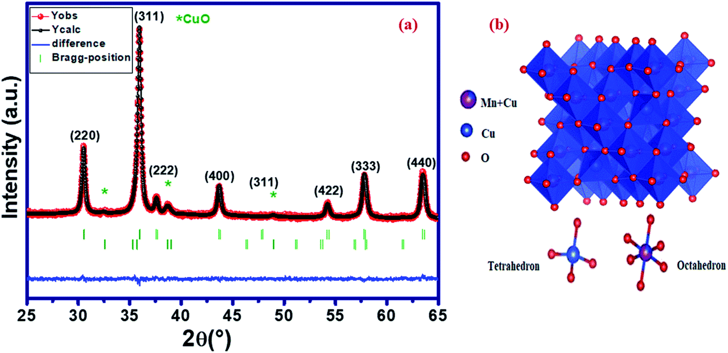


 there is a pure conduction process90 where the charge carriers drift to long distances. However, at the high-frequency region it is at frequencies above the maximum peak
  the carriers are spatially constrained to move freely only within their potential wells over short distances.91 The M′′(f) experimental data have been adjusted according to the Bergman proposed Kohlrausch, Williams and Watts (KWW) function:92
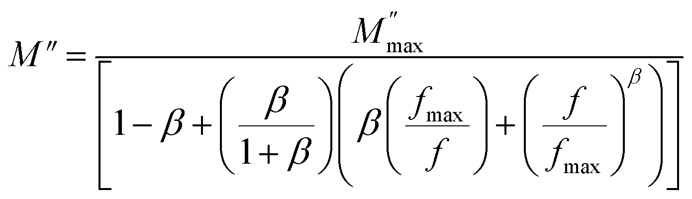
 is the peak maxima, fmax is its corresponding frequency and β is the stretching factor (0 < β < 1), which indicates a Debye or non-Debye type of the dielectric relaxation.93 As per eqn (38), the parameters obtained from the fitted data of M′′(f) at different temperatures for our compound are collated in Table 4. We thus notice that all values of β are less than unity. This confirms the non-Debye behavior for the Cu1.5Mn1.5O4 compound. We plotted in Fig. 13c the variation in Ln(fmax) vs. 1000/T, where fmax is the frequency at which the maximum of M′′ occurs in order to estimate the activation energy of the contributions for the Cu1.5Mn1.5O4 compound. The obtained curve obeys the Arrhenius law. The obtained values of the activation energy revealed that R1 is 0.09 eV and R2 is 0.134 eV. It was found that our results confirm those obtained from the imaginary part of the impedance Z′′ and justify the goodness of both adjustments of M′′ vs. frequency and Nyquist curves. Fig. 13d shows the Argand plot for electric modulus (M′′ vs. M′) at different temperatures of the Cu1.5Mn1.5O4 sample. We observe a single semicircle associated with the grain effect. When the temperature increases, this semicircle transforms from a closed semicircle to an arc. Here, in the M′′ vs. M′ plot, the existence of non-semicircles indicates non-Debye-type relaxation.