
 Open Access Article
 This Open Access Article is licensed under a Creative Commons Attribution-Non Commercial 3.0 Unported Licence
A 3-D NanoMagnetoElectrokinetic model for ultra-high precision assembly of ferromagnetic NWs using magnetic-field assisted dielectrophoresis
Sachin K. Singh a,
Md Mahadi Rajibb,
Justine L. Drobitchc,
Jayasimha Atulasimhab,
Supriyo Bandyopadhyayc and
Arunkumar Subramanian*a
a,
Md Mahadi Rajibb,
Justine L. Drobitchc,
Jayasimha Atulasimhab,
Supriyo Bandyopadhyayc and
Arunkumar Subramanian*a
aDepartment of Mechanical and Industrial Engineering, University of Illinois at Chicago, Chicago, IL 60607, USA. E-mail: sarun@uic.edu
bDepartment of Mechanical and Nuclear Engineering, Virginia Commonwealth University, Richmond, VA 23284, USA
cDepartment of Electrical and Computer Engineering, Virginia Commonwealth University, Richmond, VA 23284, USA
First published on 30th October 2020
Abstract
This report presents a three-dimensional (3-D) magnetoelectrokinetic model to investigate a new approach to magnetic-field assisted dielectrophoresis for ultra-high precision and parallel assembly of ferromagnetic Ni nanowires (NWs) on silicon chips. The underlying assembly methodology relies on a combination of electric and magnetic fields to manipulate single nanowires from a colloidal suspension and yield their assembly on top of electrodes with better than 25 nm precision. The electric fields and the resultant dielectrophoretic forces are generated through the use of patterned gold nanoelectrodes, and deliver long-range forces that attract NWs from farther regions of the workspace and bring them in proximity to the nanoelectrodes. Next, magnetic-fields generated by cobalt magnets, which are stacked on top of the gold nanoelectrodes at their center and pre-magnetized using external magnetic fields, deliver short range forces to capture the nanowires precisely on top of the nanomagnets. The 3-D NanoMagnetoElectrokinetic model, which is built using a finite element code in COMSOL software and with further computations in MATLAB, computes the trajectory and final deposition location as well as orientation for all possible starting locations of a Ni NW within the assembly workspace. The analysis reveals that magnetic-field assisted dielectrophoresis achieves ultra-high precision assembly of NWs on top of the cobalt nanomagnets from a 42% larger workspace volume as compared to pure dielectrophoresis and thereby, establishes the benefits of adding magnetic fields to the assembly workspace. Furthermore, this approach is combined with a strategy to confine the suspension within the reservoir that contains a high density of favorable NW starting locations to deliver high assembly yields for landing NWs on top of contacts that are only twice as wide as the NWs.
Introduction
Controlled manipulation of nanomaterials is a highly challenging, yet important task in the field of nanotechnology, especially owing to a continued emphasis on miniaturization of devices across several fields of engineering. Of the many techniques commonly used for nanomaterial manipulation and integration onto micro- and nano-devices, dielectrophoresis (DEP) or field-directed, bottom-up assembly of one-dimensional nanomaterials has gained significant research attention. It has enabled batch-scale deposition of nanowires (NWs)/nanotubes across target electrodes in application areas spanning nanoelectronics,1,2 energy storage,3 field effect transistors,4 and sensors,5,6 among others. DEP relies on the polarization of nanomaterials under non-uniform electric fields and enables the deposition of any material system onto a target substrate as long as its polarizability is sufficiently different from that of the underlying suspension medium. A key and as-yet unaddressed challenge associated with DEP assembly of nanowires is its inability to precisely control the final landing location and orientation of a nanowire/nanotube on its target substrate. Specifically, the assembled NW lands not exactly at the centre, but at any spot on a much wider electrode pair, which typically measures hundreds of nanometers to several microns in width as opposed to the NW diameter in the tens of nanometers range. This has limited the application of DEP in devices that require high precision control over deposition such as in the fabrication of quantum nanoelectronic7 and bioelectronic8 devices.In addition to DEP, there have also been reports, although with a varying degree of success, on high precision assembly of NWs and NTs through other methods such as self-assembly,9 controlled capillary flow,10,11 patterning regions for selective interaction on substrate,12,13 and dip-pen nanolithography.14 One such technique is magnetic field directed deposition of nanowires.15,16 This technique involves controlled manipulation of NWs through magnetic fields that are created either by external magnets15 or by magnetized contact pads/electrodes, to produce micro- and nano-devices. A key requirement in this technique is that the NW either contains capped magnetic ends17 or is itself magnetic in nature.16 This method of magnetic field directed assembly of nanowires has found application in fabrication of transparent conductive thin films,18 biosensors,19 ultra-high density recording devices,20 and biomedical applications.21,22 Further, the manipulation of nanostructures by magnetic fields has several benefits,23 which include: (i) the nanomaterial response to the assembly field can be tuned by changing its magnetic properties, (ii) similar to electric field, the magnetic field offers a non-invasive means of manipulating nanomaterial, (iii) magnets (permanent and electromagnetic) are readily available in a range of strengths commercially, and (iv) in contrast to electric fields, magnetic fields don't induce any current in the suspension solution, and are insensitive to surface charge or pH. However, magnetic assembly of nanomaterials also faces challenges, which are similar to those of DEP, in achieving high assembly precision.
This report addresses this challenge and presents a magnetic-field assisted DEP technique, which helps improve the precision of nanowire placement on the target electrodes, for the first time. Specifically, the electric field component enables the long-range manipulation of the nanowires within the assembly workspace, while the magnetic-field component (generated through magnetized contacts) is used for short-range localization of the nanowires within an ultra-small area of the target electrodes. This strategy has been analysed using a new three-dimensional computational model that captures the underlying NanoMagnetoElectrokinetic system. This model has evolved from a nanoelectrokinetic model, which was presented in a past report to study the manipulation of single nanowires on silicon chips using floating electrode DEP (FE-DEP).24,25 FE-DEP is a variant of the DEP nanoassembly process, where one of the two assembly electrodes is biased against a grounded electrode (usually the underlying substrate), while the other assembly electrode is held at a floating potential. This is unlike conventional DEP where the assembly bias is applied directly on the assembly electrode pair and enables a higher yield of single NW assembly with FE-DEP since it substantially slows the capture of subsequent NWs after the deposition of the first nanowire at electrodes.25 The NanoMagnetoElectrokinetic model presented in this paper predicts the path of motion of a NW during magnetic field assisted DEP, its final deposition location/orientation, and the region of interest for targeted NW deposition onto nanoelectrode pairs. Furthermore, it demonstrates the ability of this combined magnetic plus FE-DEP based assembly to position single nanowires on top of their assembly electrodes with high-throughput and with ultra-precision (better than 25 nm) in a self-limiting fashion. In addition, a strategy involving a patterned resist layer is presented to confine the NW suspension to a workspace volume that preferentially yields such ultra-high precision assembly and provides pointers for the future experimental realization of this methodology. This investigation on magnetic-field assisted FE-DEP nanoassembly has been performed using magnetized nickel NWs as the model material system. This choice of nickel NWs has been motivated by its relevance for next generation applications involving nanoelectronics26 and sensing.27 Furthermore, Ni nanowires of uniform diameter are very easy to synthesize using electrodeposition of Ni into nanoporous anodic alumina templates.28 These nanowires can be harvested and dispersed in an ethanol solution by first dissolving out the surrounding alumina matrix in hot chromic–phosphoric acid and then immersing the substrate containing the released nanowires in the ethanol solution while agitating the solution ultrasonically. This method has been practised by us to produce un-agglomerated NWs dispersed in the ethanol solution.
Magnetic-field assisted FE-DEP
The proposed magnetic-field assisted FE-DEP chip design and the resulting nanoassembly process is illustrated in Fig. 1. The assembly chip is comprised of a silicon substrate, which is coated on its surface with a 200 nm thick, insulating silicon nitride layer. On top of the nitride layer, a nanoelectrode stack is defined and is comprised of two layers: (a) a bottom gold nanoelectrode pair to generate an inhomogenous electric field, which has its maxima on the electrode surface and manipulates NWs over a long-range, and (b) a top cobalt nanomagnet pair to generate magnetic fields that manipulate NWs over a shorter range in proximity to the electrodes. In the designs employed within this effort, the gold nanoelectrode and cobalt nanomagnet widths were set at 250 nm and 100 nm, respectively. Here, an external magnetizing field is first employed to magnetize the cobalt nanomagnets in a specific direction prior to start of the assembly. The cobalt electrodes are engineered with shape anisotropy (where their length at 250 nm is 2.5 times their 100 nm width) and hence, the resulting magnetic moment is aligned along their easy axes (i.e., their longitudinal direction) with a high magnetic field directed along the easy axes. As long as the sizes of the nanomagnets are large enough that they remain ferromagnetic and do not turn super-paramagnetic, the nanomagnets retain their magnetized state even after the magnetic field is removed. Next, a homogenous colloidal suspension of Ni nanowires in ethanol, which is typically prepared and homogenized through ultrasonication, is placed on the silicon chip with the pre-patterned nanoelectrode stack. After placing the suspension on the chip, an AC assembly bias is applied to one of the gold nanoelectrodes (Fig. 1(a)). The opposing electrode is held at a floating potential with respect to the underlying substrate, which is electrically grounded. Thus, the electrical circuit during FE-DEP involves an additional capacitive impedance between the floating and ground electrodes. This impedance becomes comparatively larger than that between the electrode pairs upon capture of a nanowire at the assembly site and thereby, substantially slows down the capture of additional nanowires beyond the first deposition, unless the suspension concentration and/or assembly bias are high enough to yield near-simultaneous assembly of multiple nanowires. When an electric field is applied across the electrodes through the generation of an electrical bias, the NWs in the suspension are polarized and get attracted towards the electric field maxima, which are located near the electrode surfaces. These electric fields exert their influence on NWs over a large region of the assembly workspace and serve to bring the nanowires in proximity to the electrode stack. Upon entry into the short-range workspace of the electrode stack, the magnetic forces/torques exerted by the cobalt nanomagnets on the ferromagnetic Ni NWs dominate over their DEP counterparts and enable the final alignment of the NWs precisely on top of the Co nanomagnets. After the nanowires are localized on the electrodes, the suspension is removed by nitrogen blow-drying and the trapped nanowires are held in place through van-der Waals interactions with the electrode surface. The inset in Fig. 1(a) shows the top view (TV) of NW deposition during magnetic-field assisted FE-DEP, illustrating the desired capture of single NWs. In the case of the 50 nm diameter NWs employed in this effort, a successful deposition on top of the Co nanomagnets results in a assembly precision better than 25 nm. However, pure FE-DEP alone, which is illustrated in Fig. 1(b), is inefficient for high precision localization of NW at the centre of the electrode pair and may deposit the NW anywhere across the width of the electrode pair (see TV in inset of Fig. 1(b)). This precise localization of nanowires right at the center of the electrodes represents a substantive improvement over the assembly precision that is typically attained using pure FE-DEP.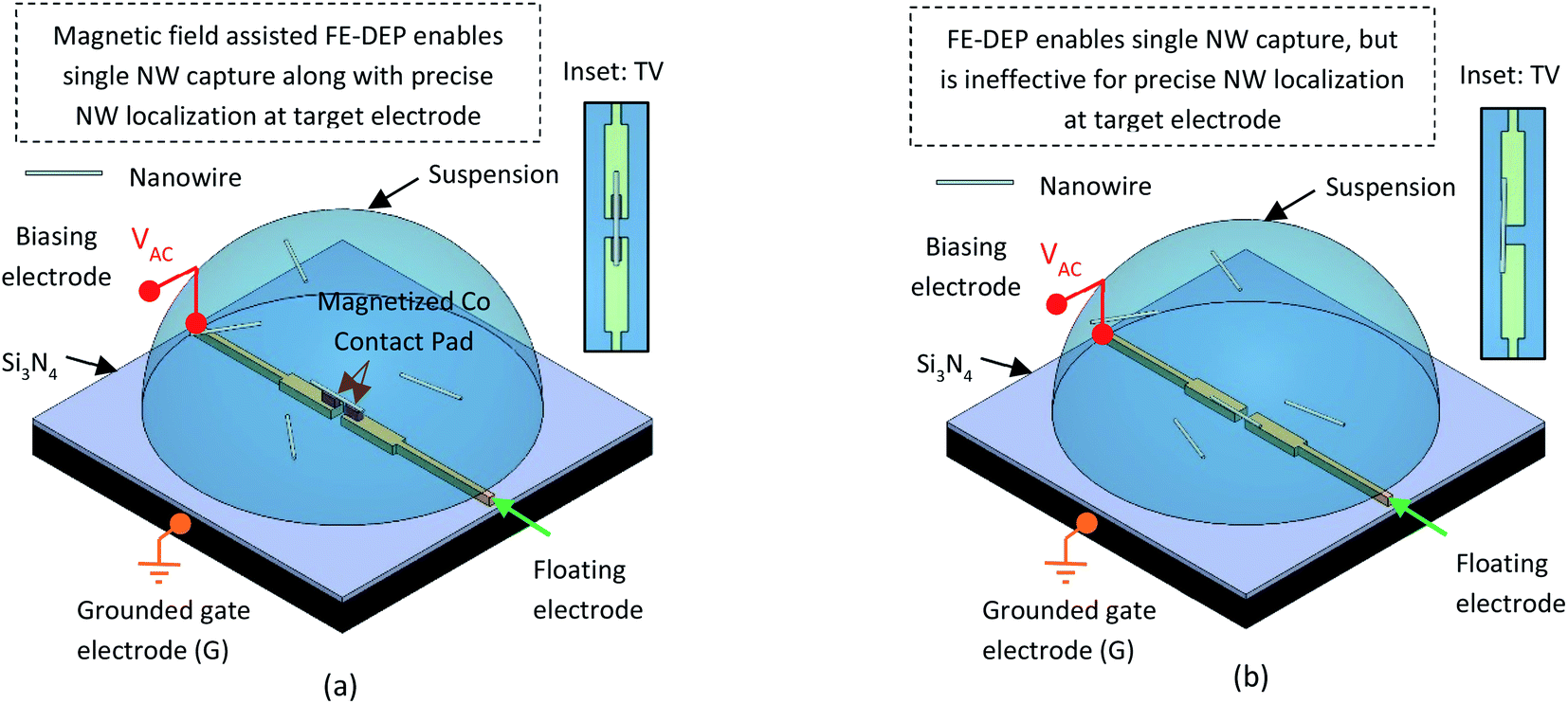 | ||
| Fig. 1 Schematic diagram of an on-chip platform based on: (a) magnetic field assisted floating electrode DEP design, (b) floating electrode DEP design. The inset in (a) and (b) show the Top View (TV) of respective NW deposition from magnetic field assisted FE-DEP and FE-DEP process. | ||
3-D NanoMagnetoElectrokinetic model
A 3-D NanoMagnetoElectrokinetic model has been built for understanding the on-chip manipulation of ferromagnetic NWs using magnetic-field assisted FE-DEP directed assembly. In this approach, the electric and magnetic fields generated by the nanoelectrode pairs and the cobalt nanomagnets are simulated using a FEM model in COMSOL Multiphysics 5.4 software. These fields are shown in Fig. 2(a), (b), (c) and (d), respectively. It is important to note that the magnetic field distribution of Fig. 2(c) and (d) imposes magnetic forces and torques on the NW during its assembly process. In order to study and assess the impact of the magnetic-field component on the assembly process, a pure FE-DEP analysis was also performed using the same electrode design.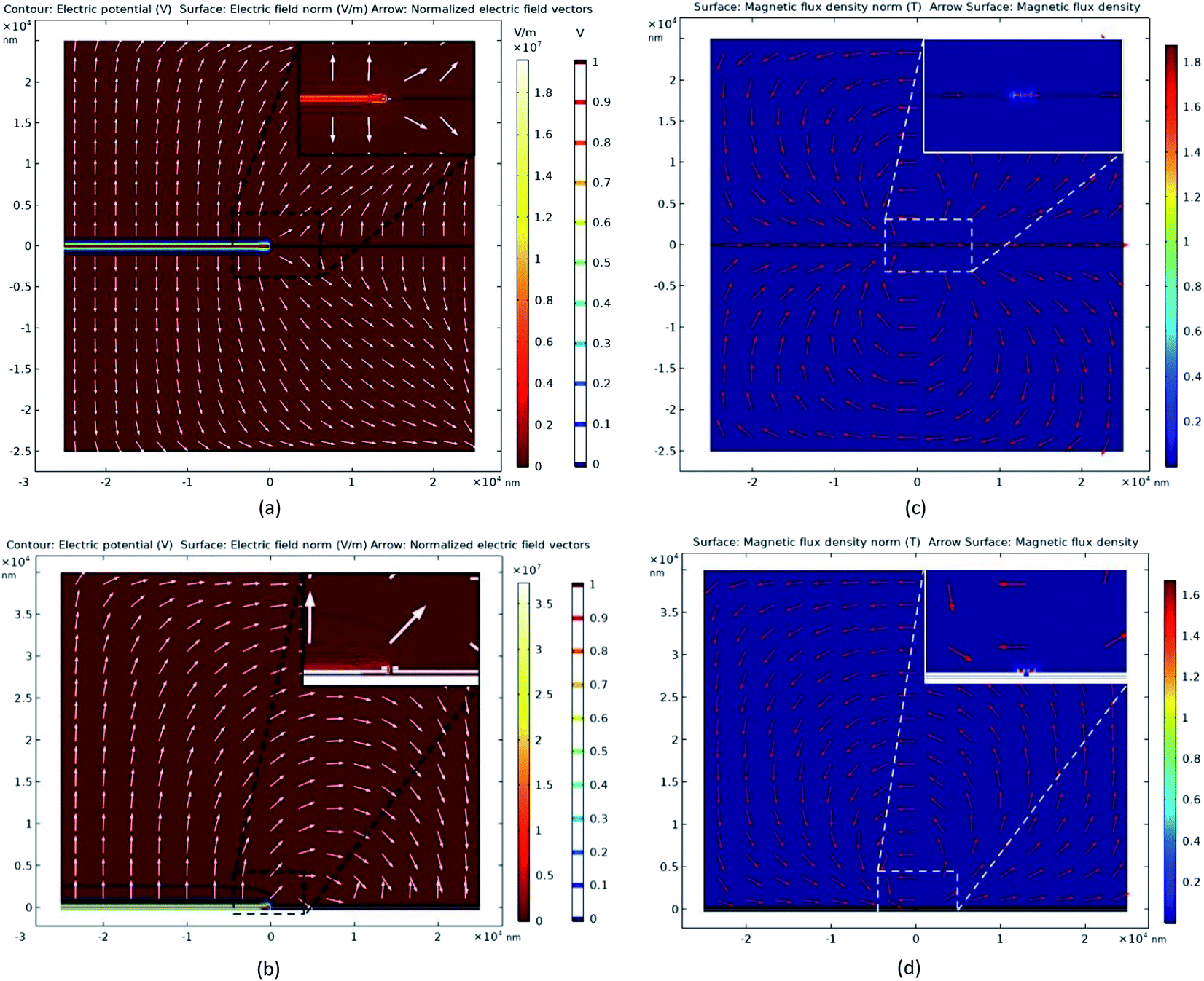 | ||
| Fig. 2 (a) Top view and (b) side view of electric field distribution within the simulation workspace, and (c) top view and (d) side view of magnetic field density distribution within the simulation workspace. The inset in each image shows that the field maxima in the inter-electrode gap region is located asymmetrically near the biasing electrode for electric field and symmetrically for the magnetic field. | ||
The simulation workspace consists of a 50 μm × 50 μm × 40 μm region on top of a 200 nm silicon nitride layer and the nanoelectrode stack is located at the center of this workspace. The bottom of this silicon nitride layer is grounded. The medium through which electric and magnetic fields are calculated is composed of ethanol suspension. The outer boundaries of the simulation workspace are maintained at zero charge boundary conditions, which lead to a replication of the electrode pairs into a longitudinal array design over the on-chip platform. The workspace size has been chosen big enough so that its boundary conditions have an insignificant effect on the electric and magnetic fields generated in proximity to the electrode stack. It can be seen from Fig. 2 that maxima of electric and magnetic fields are located around the inner edges of the electrode stack. Furthermore, the distribution of electric fields is asymmetric with regards to the nanoelectrode pair, while that of the magnetic fields is approximately symmetric with respect to Co nanomagnet pair. This causes the electric forces to be directed asymmetrically towards the biasing electrode.
The electric field, which is computed by the FEM model, is then used in a MATLAB R2019b script to calculate the DEP forces, which act on a nickel NW within the simulation workspace. The underlying computational procedure has been described elsewhere in our previous report.24 To calculate the electric forces, the NWs are assumed to be a prolate ellipsoid along which the applied electric field is constant and invariant. The time averaged value of this DEP force is given as:25
 | (1) |
 | (2) |
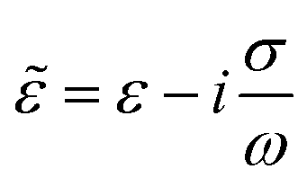
![[small epsilon, Greek, tilde]](https://www.rsc.org/images/entities/i_char_e0de.gif) NW and m are the complex permittivities of the NW and suspension medium, respectively. The variation of the CM factor as a function of the biasing frequency is shown in Fig. 3 for the Ni NW suspension in ethanol. The complex permittivities of the NW/medium are calculated based on their dielectric permittivity (ε), conductivity (σ) and applied frequency (ω) of electric field:
NW and m are the complex permittivities of the NW and suspension medium, respectively. The variation of the CM factor as a function of the biasing frequency is shown in Fig. 3 for the Ni NW suspension in ethanol. The complex permittivities of the NW/medium are calculated based on their dielectric permittivity (ε), conductivity (σ) and applied frequency (ω) of electric field:
 | (3) |
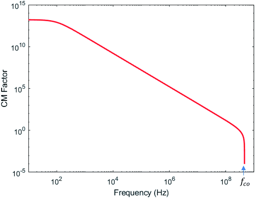 | ||
| Fig. 3 Clausius–Mossotti factor as a function of frequency for Ni NWs in an ethanol suspension. | ||
Both the electric and magnetic field components of the model assume a suspension of magnetized nickel NWs (with a nominal diameter of 50 nm and length of 1 μm) in ethanol. In these simulations, we have assumed the following values for the material properties: εNW, εm, σNW, and σm have values of 5.13 × 10⁻¹¹ F m−1, 2.17 × 10⁻¹⁰ F m−1, 2.19 × 10⁶ S m−1, and 1.35 × 10⁻⁷ S m−1, respectively. The NWs are more polarizable than the suspension medium and are therefore attracted towards the electric field maxima located at the inner edge of the biasing electrode. This phenomenon of NW attraction towards biasing electrodes (positive DEP) is observed at frequencies (ω) below the crossover frequency (fCO), which is shown in Fig. 3. From this figure, it can be seen that the Clausius–Mossotti (CM) factor turns negative at frequencies higher than 2 × 10⁸ Hz, which would result in negative DEP and a repulsion of NWs from regions of electrode field maxima, i.e. away from the biasing electrodes. In these calculations, we have chosen a frequency of 10 MHz to insure operation in the positive DEP regime with forces that are reasonable enough to achieve controlled NW deposition within a few seconds to a few minutes.
The magnetic force exerted by cobalt nanomagnets (with a magnetization of 1.45 × 10⁶ A m−1) on a Ni NW can be calculated as:31
![[F with combining right harpoon above (vector)]](https://www.rsc.org/images/entities/i_char_0046_20d1.gif) MAG = ∇( MAG = ∇(![[M with combining right harpoon above (vector)]](https://www.rsc.org/images/entities/i_char_004d_20d1.gif) NW · NW · ![[B with combining right harpoon above (vector)]](https://www.rsc.org/images/entities/i_char_0042_20d1.gif) ) )
| (4) |
NW is the magnetic moment of the nickel NW and is the magnetic flux density created by cobalt contact pads.
Assuming that the magnetic moment NW is spatially uniform across the NW, the magnetic force simplifies to:
|
MAG = NW · ∇
| (5) |
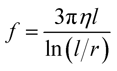
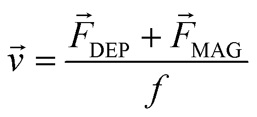
The motion of NWs under the action of DEP and magnetic forces is resisted by frictional drag, which is induced by the viscosity of the suspension. The drag force is accounted in this model through the use of an average friction factor f, which is defined as:33
 | (6) |
 | (7) |
In addition to forces, the non-uniform electric and magnetic fields also induce electro- and magneto-orientation torques (Tz-DEP and Tz-MAG, respectively) on the NW during its motion towards the electrodes. These torques are calculated as:
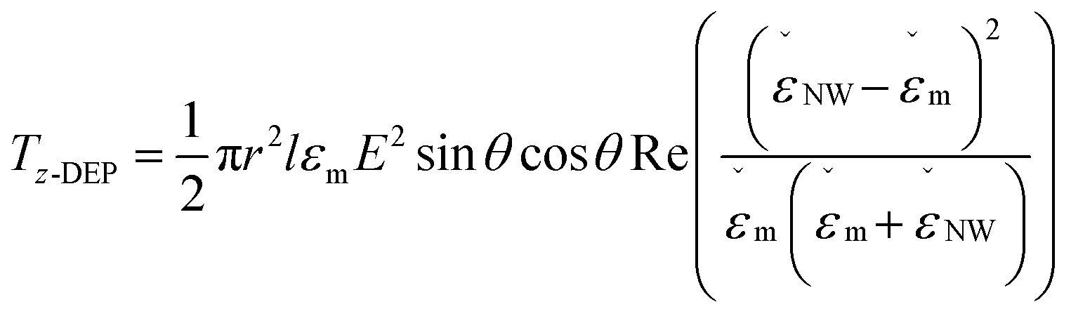 | (8) |
|
Tz-MAG = NW ×
| (9) |
For simplicity, we have only considered the NW torques in X–Y plane (i.e., about the z-axis). Similar to the translational motion of the NW, its rotation also depends on the frictional drag torque induced by suspension medium. The rotational frictional factor (fθ) experienced by the NW is calculated as:33
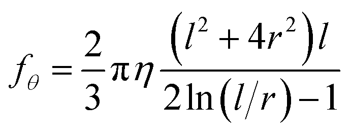 | (10) |
Thereafter, the angular velocity of the NW at different locations in the simulation workspace is calculated as:
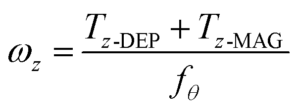 | (11) |
Eqn (7) and (11) are utilized in the MATLAB script to calculate the NW translational and rotational velocities at various nodes in the computational workspace. These velocities are then used to compute the NW trajectorie, its eventual trapping location and orientation, and the deposition time. Note that the assembly orientation of a NW is dependent on its initial orientation in the suspension medium. As the initial orientation is unknown, we have assumed the NW to be oriented along the electric field vectors at the start of the assembly process, and the orientation of NW changes according to eqn (11) during its transport towards the eventual localization location.
Results and discussion
To understand the impact of the magnetic-field component on the assembly process, we have computed the trajectory and final deposition location/orientation for NWs starting from all locations (mesh nodes) within the simulation workspace for both assembly methods: pure FE-DEP and magnetic field assisted FE-DEP. The deposition of NWs on electrode sites is found to predominantly occur in four configurations: cantilevered deposition on the biasing electrode, cantilevered deposition on the floating electrode, bridging deposition on top of the gold nanoelectrode pair, and bridging deposition on top of the cobalt nanomagnet pairs. In contrast to the three former configurations, the bridging deposition on top of the cobalt nanomagnets represents the desired yield for this deposition process (schematically illustrated in Fig. 1(a)). In this condition, the NW is both centrally localized and aligned in a parallel fashion with respect to the electrode stack, resulting in an assembly precision of better than 25 nm.The effect of magnetic field on dielectrophoretic assembly of nickel NWs can be visualized through the trajectories pursued by a NW from two starting locations, which are plotted in Fig. 4(a). In this figure, the NWs start from the two different locations: SL1 (3153, 0, 2277) and SL2 (4114, 25, 3588). The origin of the coordinate system is located at the centre of the electrode pair, and all coordinates are indicated in nm. It can be seen from the final NW landing location and orientation (Fig. 4(b)) that the deposition using magnetic field assisted DEP (blue NWs) results in a bridging configuration closer to the centre of the electrode stack and right on top of the Co nanomagnets, as compared to cantilevered localization on top of the biasing electrode deposition through pure FE-DEP (red NW). Furthermore, the orientation of NWs deposited using magnetic-field assisted DEP are more closely aligned to the electrode pair axis as compared to that observed with a pure FE-DEP deposition process. This is due to the short-range magnetic forces and torques imposed by the nanomagnets on the ferromagnetic NWs during their transport through the suspension. These forces and torques sufficiently enable changes to the NW trajectory and its landing position/orientation, and ultimately lead to an improvement in ultra-high precision assembly of NWs for the starting locations under consideration in Fig. 4.
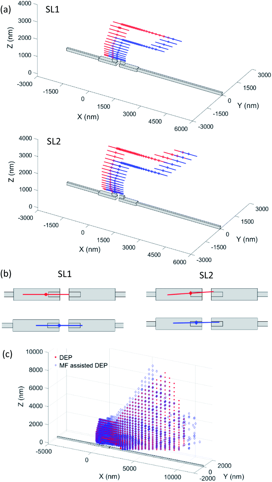 | ||
| Fig. 4 (a) Trajectories followed by NWs starting from two locations [SL1 (3153, 0, 2277) and SL2 (4114, 25, 3588)] in the simulation workspace during pure FE-DEP (red NWs) and magnetic-field assisted FE-DEP (blue NWs); (b) corresponding final deposition location and orientation for NWs starting from SL1 and SL2; and (c) starting workspace locations that yield high precision NW deposition on Co nanomagnets in a bridging configuration within 30 seconds. | ||
To quantitatively compare the effectiveness of magnetic field assisted FE-DEP and pure FE-DEP for NW localization with a precision better than 25 nm, we have computed all the starting locations for NWs that ultimately lead to bridging NW deposition within the central 100 nm wide region of the electrode stack (i.e., on top of the nanomagnets) over a 30 second assembly time period. These results are plotted in Fig. 4(c). It is found that magnetic field assisted DEP successfully captures NWs from more starting locations within the simulation workspace than the pure FE-DEP process. Furthermore, the total capture volume (or, the assembly workspace volume) for successful ultra-high precision assembly is calculated for both methods by adding the volume of each mesh element that yields successful NW deposition. It is found that the capture volume increases from 3.89 × 10⁹ nm3 for pure FE-DEP to 5.53 × 10⁹ nm3 for magnetic-field assisted FE-DEP, which represents a 42% improvement in total capture volume for a 30 second nanoassembly process. Therefore, magnetic field assisted DEP offers a much higher probability for ultra-high precision NW deposition as compared to pure FE-DEP.
With the establishment of favourable performance through the use of magnetic-field assisted FE-DEP, we now present a method to estimate and optimize the yield of successful NW deposition on top of cobalt nanomagnets using this approach. In a past report,24 we had presented a method involving the use of patterned resist wells or reservoirs that confine the nanowire suspension to stay within regions that present a high density of starting locations that yield successful FE-DEP assembly. It is clear from Fig. 4(c) that in order to yield NW deposition on Co nanomagnets in a bridging configuration using magnetic-field assisted DEP, the NWs have to start predominantly from regions above the floating electrode and very few locations over the biasing electrode lead to such successful assembly outcomes. This asymmetric nature of the NW sourcing volume can be used to design a fluidic reservoir that allows a higher yield of NWs assembling on top of the Co nanomagnets. A representative cuboid resist reservoir and the corresponding capture volume within the reservoir leading to NW deposition on Co nanomagnets are shown in Fig. 5(a). The fluidic reservoir represents the volume within which the suspension needs to be confined in order to improve yields for NW assembly on contact pads. It can be created by lithographically patterning a reservoir within a photoresist layer which confines the NW suspension within that reservoir region, as shown in Fig. 5(b). The reservoir is positioned asymmetrically over the floating electrode region in order to predominantly encompass the favoured starting NW locations (as shown in Fig. 4(c)) and has dimension of 6400 nm × 200 nm × 4000 nm. We can calculate the corresponding assembly yields by computing the ratio of total NW capture volume shown in Fig. 5(a) to the total reservoir volume. It is found that a 49% yield can be achieved for NW deposition on top of Co nanomagnets through the use of magnetic field assisted FE-DEP. While this number is lower than the ∼80% yields achieved in previous reports for the assembly of NWs through pure FE-DEP, it is important to note that those results considered assembly within microscopically wide electrodes as successful outcomes for the manipulation process. On the other hand, the presented methodology yields assembly with better than a 25 nm precision and hence, represents a substantive advance over pure electric field driven assembly approaches.
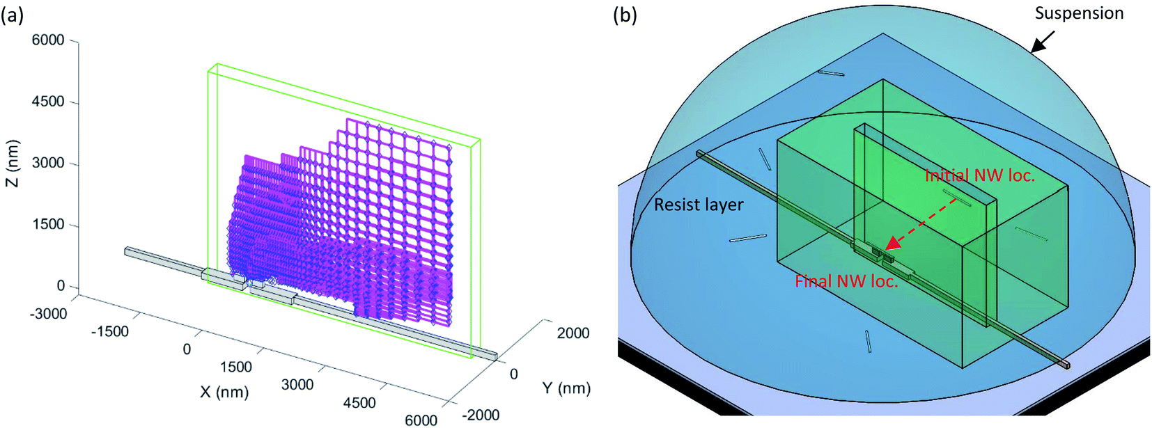 | ||
| Fig. 5 (a) Resist reservoir volume (green) and volume corresponding to each starting location within the reservoir that leads to NW deposition in a bridging configuration at cobalt nanomagnets after 30 seconds of magnetic field assisted DEP (magenta), and (b) schematic illustration of the patterned resist layer that preferentially sources NWs from starting locations that yield ultra-high precision assembly. | ||
Conclusions
A 3-D NanoMagnetoElectrokinetic model is presented to investigate an ultra-high precision method for assembly of ferromagnetic NWs. The assembly method involves a combination of FE-DEP and magnetic-field driven forces and torques to centre and align NWs on an on-chip platform. The numerical model computes the forces and torques imposed on the NW within the assembly workspace and yields their three-dimensional trajectory as well as final landing location/orientation. Through the use of the NanoMagnetoElectrokinetic model, magnetic-field assisted FE-DEP is demonstrated to localize 50 nm diameter ferromagnetic NWs on top of 100 nm wide Co nanomagnetic pads from a much higher number of workspace starting locations as compared to pure FE-DEP (a 42% improvement in volume). A larger sourcing volume and higher precision for bridging deposition of ferromagnetic NWs onto contact pads makes this method better suited for next-generation nanoelectronics and sensing applications, which would benefit from such high precision assembly of NWs. Finally, this assembly method is employed alongside a strategy to confine the NW suspension to remain within favourable regions of the workspace (from the perspective of yielding assembly in the desired ultra-high precision configuration) to enable competitive assembly yields for this deposition process.Conflicts of interest
There are no conflicts to declare.Acknowledgements
A. S. and S. K. S. also acknowledge support, in part, from the National Science Foundation under Grant No. 1655496 and 1661038. The electrokinetics module used in the presented NanoMagnetoElectrokinetic modeling framework was developed with support from these grants.References
- A. Rotaru, J. Dugay, R. P. Tan, I. A. Guralskiy, L. Salmon, P. Demont, J. Carrey, G. Molnar, M. Respaud and A. Bousseksou, Adv. Mater., 2013, 25, 1745 CrossRef CAS.
- S. Schuerle, M. K. Tiwari, K. Shuo, D. Poulikakos and B. J. Nelson, Microelectron. Eng., 2011, 88, 2740 CrossRef CAS.
- A. Subramanian, N. S. Hudak, J. Y. Huang, Y. Zhan, J. Lou and J. P. Sullivan, Nanotechnology, 2014, 25, 265402 CrossRef CAS.
- P. Stokes and S. I. Khondaker, Nanotechnology, 2008, 19, 175202 CrossRef.
- S. K. Jangir, H. K. Malik, P. Saho, R. Muralidharan, T. Srinivasan and P. Mishra, Nanotechnology, 2019, 30, 105706 CrossRef CAS.
- C. G. Nunez, A. F. Brana, N. Lopez, J. L. Pau and B. J. Garcia, Nanotechnology, 2020, 31, 225604 CrossRef CAS.
- H. Yan, H. S. Choe, S. W. Nam, Y. Hu, S. Das, J. F. Klemic, J. C. Ellenbogen and C. M. Lieber, Nature, 2011, 470, 240 CrossRef CAS.
- S. Fringes, C. Schwemmer, C. D. Rawlings and A. W. Knoll, Nano Lett., 2019, 19, 8855 CrossRef CAS.
- B. D. Gates, Nat. Nanotechnol., 2010, 5, 484 CrossRef CAS.
- K. Oh, J.-H. Chung, J. J. Riley, Y. Liu and W. K. Liu, Langmuir, 2007, 23, 11932 CrossRef CAS.
- E. M. Freer, O. Grachev, X. Duan, S. Martin and D. P. Stumbo, Nat. Nanotechnol., 2010, 5, 525 CrossRef CAS.
- M. Li, R. B. Bhiladvala, T. J. Morrow, J. A. Sioss, K.-K. Lew, J. M. Redwing, C. D. Keating and T. S. Mayer, Nat. Nanotechnol., 2008, 3, 88 CrossRef CAS.
- C. R. Barry and H. O. Jacobs, Nano Lett., 2006, 6, 2790 CrossRef CAS.
- J.-H. Lee, C. K. Najeeb, G.-H. Nam, Y. Shin, J.-H. Lim and J.-H. Kim, Chem. Mater., 2016, 28, 6471 CrossRef CAS.
- C. M. Hangarter, Y. Rheem, B. Yoo, E.-H. Yang and N. V. Myung, Nanotechnology, 2007, 18, 205305 CrossRef.
- M. Beheshti, J. Choi, X. Geng, E. P. Murphy and S. Park, Microelectron. Eng., 2018, 193, 71 CrossRef CAS.
- C. M. Hangarter and N. V. Myung, Chem. Mater., 2005, 17, 1320 CrossRef CAS.
- O. Trotsenko, A. Tokarev, A. Gruzd, T. Enright and S. Minko, Nanoscale, 2015, 7, 7155 RSC.
- J. Jimenez, R. Sheparovych, M. Pita, A. N. Garcia, E. Dominguez, S. Minko and E. Katz, J. Phys. Chem. C, 2008, 112, 7337 CrossRef CAS.
- M. Gong, J. Zhang and S. Ren, Nanotechnology, 2018, 29, 345602 CrossRef.
- A. Hultgren, M. Tanase, C. S. Chen, G. J. Meyer and D. H. Reich, J. Appl. Phys., 2003, 93, 7554 CrossRef CAS.
- Y. P. Ivanov, A. Alfadhel, M. Alnassar, J. E. Perez, M. Vazquez, A. Chuvilin and J. Kosel, Sci. Rep., 2016, 6, 24189 CrossRef CAS.
- R. S. M. Rikken, R. J. M. Nolte, J. C. Maan, J. C. M. van Hest, D. A. Wilson and P. C. M. Christianen, Soft Matter, 2014, 10, 1295 RSC.
- S. K. Singh, N. Aryaan, M. R. A. Shikder, B. W. Byles, E. Pomerantseva and A. Subramanian, Nanotechnology, 2019, 30, 025301 CrossRef.
- N. K. R. Palapati, E. Pomerantseva and A. Subramanian, Nanoscale, 2015, 7, 3109 RSC.
- J. Kim, W. J. D. Silva, A. R. B. M. Yusoff and J. Jang, Sci. Rep., 2016, 6, 19813 CrossRef CAS.
- S. Wang, K. Chen, M. Wang, H. Li, G. Chen, J. Liu, L. Xu, Y. Jian, C. Meng, X. Zheng, S. Liu, C. Yin, Z. Wang, P. Du, S. Qu and C. W. Leung, J. Mater. Chem. C, 2018, 6, 4737 RSC.
- H. Zeng, R. Skomski, L. Menon, Y. Liu, S. Bandyopadhyay and D. J. Sellmyer, Phys. Rev. B, 2002, 65, 134426 CrossRef.
- S. Raychaudhuri, S. A. Dayeh, D. Wang and E. T. Yu, Nano Lett., 2009, 9, 2260 CrossRef CAS.
- L. Liu, K. Chen, N. Xiang and Z. Ni, Electrophoresis, 2019, 40, 873 CrossRef CAS.
- D. J. Griffiths, Introduction to Electrodynamics, Prentice Hall, 1999 Search PubMed.
- R. E. Hummel, Electronic Properties of Materials, Springer, 2001 Search PubMed.
- E. W. Small and I. Isenberg, Biopolymers, 1977, 16, 1907 CrossRef CAS.
| This journal is © The Royal Society of Chemistry 2020 |