DOI:
10.1039/D0RA08211B
(Paper)
RSC Adv., 2020,
10, 41755-41763
Room temperature synthesis of BiOBr1−xIx thin films with tunable structure and conductivity type for enhanced photoelectric performance
Received
25th September 2020
, Accepted 7th November 2020
First published on 16th November 2020
Abstract
The surface states of semiconductors determine the semiconductor type. Although BiOCI, BiOBr and BiOI all belong to the bismuth oxyhalide semiconductor family and have similar crystal structures and electronic structures, they exhibit different conductivity types due to their respective surface states. In this paper, a modified successive ionic layer adsorption and reaction (SILAR) method was developed to fabricate I-doped BiOBr1−xIx nanosheet array films on FTO substrates at room temperature for the first time. Interestingly, the properties of p-type BiOBr were changed by doping an appropriate amount of iodine into a BiOBr film to form an n-type BiOBr1−xIx thin film. The I-doped BiOBr1−xIx (x = 0.2, 0.4, 0.5) nanosheet arrays had a perfect single-crystal structure, and the dominant growth plane was (110). A higher doping amount of I led to a darker colour of the BiOBr1−xIx film and a redshift of the absorption wavelength; consequently, the bandgap value changed from 2.80 eV to 1.85 eV. The highest short-circuit current and open-circuit voltage of the solar cell based on BiOBr0.5I0.5 film could reach 1.73 mA cm−2 and 0.55 V, which was considered to be attributed to the effective light absorbance, long photogenerated charge lifetime and sufficient charge separation in the BiOBr0.5I0.5 film.
Introduction
Bismuth oxyhalides (BiOX, X = Cl, Br, I) are bismuth-based ternary compounds that have recently attracted attention because of their layered growth structure and high stability,1–5 which provide interesting potential applications in electronics, catalysis and energy storage.6–8 The BiOX materials exhibit a tetragonal matlockite structure consisting of [Bi2O2] layers sandwiched between double halide [X] layers to form [X–Bi–O–Bi–X] layers, held together by van der Waals interactions through the halogen atom along the [001] direction.9,10 The arrangement of these layers provides a large space for polarization of the atoms favourable for forming a built-in static electric field, which can promote the separation and transport of photoinduced electron–hole pairs.11 Among the bismuth oxyhalide family (BiOCl, BiOBr and BiOI), BiOCl exhibits no visible light activity owing to its wide bandgap energy (Eg = 3.5 eV).12 BiOBr and BiOI can respond to visible light, indicating the efficient conversion of solar energy, but BiOI exhibits a faster photocarrier recombination rate than BiOBr.13 To improve the BiOBr visible light absorption, some strategies have been applied, including controlling the synthesis of BiOBr with specific morphology and structure,14,15 constructing BiOBr-based composites with other semiconductors,16–18 doping with metal atoms and so on.19,20 In addition, within ion doping, self-doping of halogens (Cl, Br, I) is an effective method to strengthen the visible light utilization and overcome the drawback of the high recombination rate of electron–hole pairs. In particular, BiOMxR1−x (M, R = Cl, Br, I) composite systems have been recently synthesized, such as BiOClxI1−x,21 BiOBrxI1−x,22 BiOClxBr1−x,23,24 BiOIxBr(1−x)25 and BiO(ClBr)(1−x)/2Ix,26 which showed higher photocatalytic activities than the corresponding single components. For instance, Jia et al. synthesized a solid solution of BiOBrxI1−x and demonstrated its visible-light-induced photocatalytic properties.27 Ren et al. reported that the optimized solid solutions exhibited higher visible-light photocatalytic activities towards rhodamine-B (RhB) degradation than BiOM (M = Cl, Br, I) because of the wider visible-light absorption range and the improved separation efficiency of the photocatalytic carriers.28 Bi et al. prepared I−-doped BiOBr with tuneable photocatalytic properties by regulating the pH values of the reaction solution.29 Although successful, these reports mainly focused on the preparation and photocatalytic properties of BiOMxR1−x (M, R = Cl, Br, I) powder materials. To our best knowledge, studies regarding low-temperature synthesis of BiOMxR1−x (M, R = Cl, Br, I) films are very limited. In particular, the photoelectric properties and photogenerated charge dynamics (lifetime and separation efficiency) of BiOMxR1−x films have not been investigated. Recently, we synthesized ordered 2D BiOX (X = CI, Br, I) nanosheet array films at room temperature through a modified SILAR method,30 which is a facile, low-temperature and low-cost strategy compared to physical deposition methods.9,31
In view of the above study, we attempted to employ the SILAR method to prepare BiOBr1−xIx nanosheet array films. By changing the molar ratio of bromine and iodine, the bandgap and conductivity type of the BiOBr1−xIx films can be fine-tuned. The band edge positions of the BiOBr1−xIx films were established by UV-vis diffuse reflectance spectra and Mott–Schottky plots. The separation, transfer behaviour and lifetime of photoinduced electron–hole pairs at the surface/interface of BiOBr1−xIx films were systematically investigated by time-resolved PL (TRPL) decay spectra and transient photovoltage (TPV) techniques. The current density–voltage (J–V) characteristic curves of solar cell devices based on BiOBr1−xIx were measured using a Keithley 2400 source meter under illumination (simulated AM 1.5 sunlight), and the charge transfer mechanism in the solar cell was discussed. This work may provide a good reference for the design and synthesis of bismuth oxyhalides photoelectric films and new insights into the photoelectric mechanisms of bismuth oxyhalide heterostructures.
Results and discussion
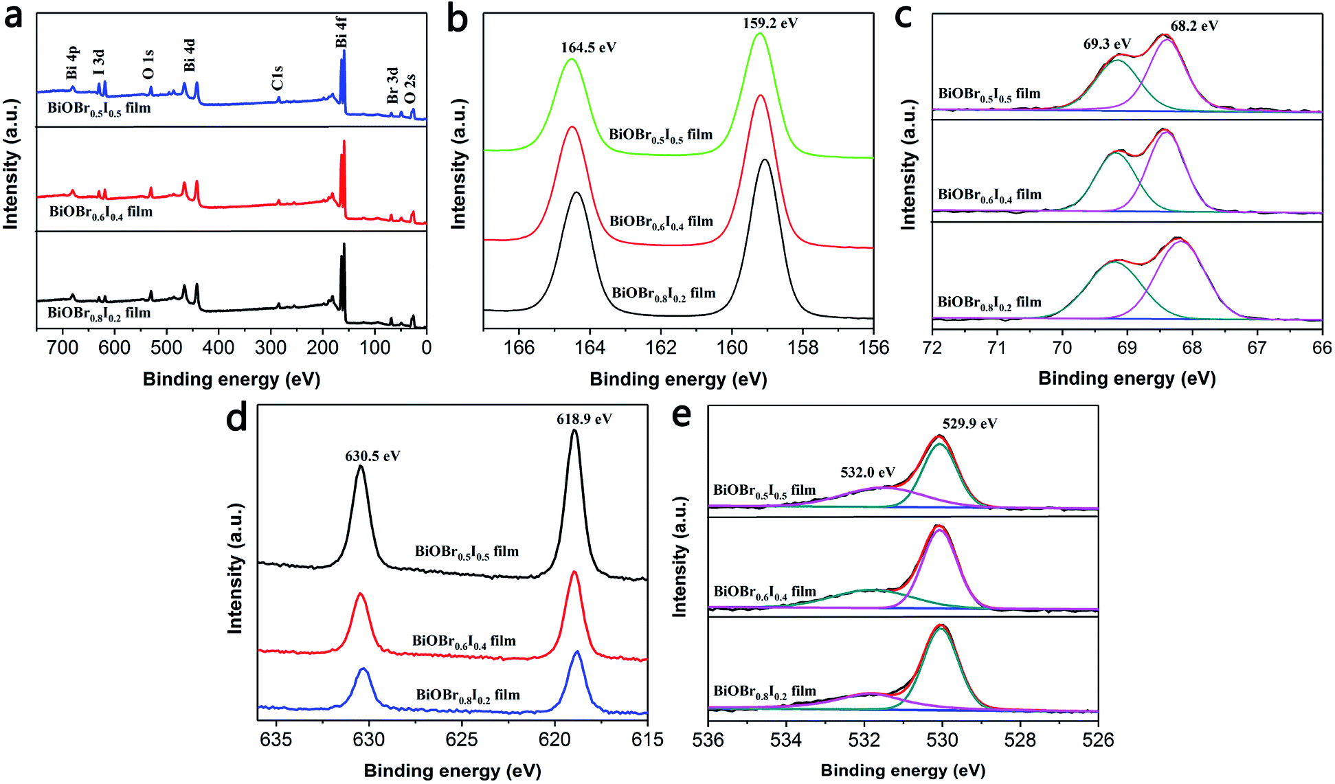
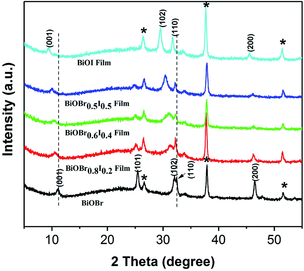
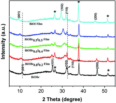
XPS was employed to characterize the surface chemical composition and valence state of the BiOBr1−xIx thin films. The XPS survey spectrum shows that Bi, O, Br and I elements coexist in all samples (Fig. 2a). Fig. 2b displays two characteristic XPS peaks located at 159.2 and 164.5 eV, which are attributed to Bi 4f7/2 and Bi 4f5/2, respectively.33,34 Thus, the chemical state of Bi was confirmed to be of +3 valency.35 Fig. 2c displays the typical Br 3d XPS spectrum. The two peaks observed at 68.2 and 69.3 eV are attributed to Br d5/2 and Br 3d3/2, corresponding to Br− in the BiOBr1−xIx films. From the high-resolution I 3d spectrum (Fig. 2d), it can be concluded that the doped I element was of −1 valency because the binding energies were located at 618.9 eV (I 3d5/2) and 630.5 eV (I 3d3/2). In the high-resolution XPS spectrum of O 1s (Fig. 2e), the main peak at 529.9 eV is attributed to Bi–O bonds in [Bi2O2]2+ slabs of the BiOBr1−xIx layered structure,36 and the peak at 532.0 eV is assigned to hydroxyl groups on the surface and other components such as OH− and H2O. According to the atomic concentrations of each element in Table 1, we calculated the actual composition ratios of Br to I in the BiOBr1−xIx films. Fig. 3 depicts the X-ray diffraction (XRD) patterns of pure BiOBr, BiOI and BiOBr1−xIx films. All the diffraction peaks for the BiOBr and BiOI films can be indexed to the tetragonal phase of BiOBr (JCPDS card no. 09-0393, a = b = 3.926 Å, c = 8.103 Å) and the tetragonal phase of BiOI (JCPDS card no. 10-445, a = b = 3.994 Å, c = 9.149 Å). The remaining diffraction peaks (labelled by asterisks) were derived from the FTO substrate (JCPDS 41-1445), and no impurity diffraction peaks were detected. In addition, the (001), (101), (102) and (110) characteristic peaks of the BiOBr1−xIx films gradually shifted to lower angles with increasing x compared to those for the pure BiOBr film. This suggests that some of the Br− ions were efficiently replaced by small amounts of I− ions,37 as the ionic radius of the I− ion is greater than that of the Br− ion (2.16 Å vs. 1.96 Å). This gradual shift in the peak positions in the XRD patterns as a function of x indicates that the BiOBr1−xIx films are solid solutions. Perceptibly, the intensity of the (101) diffraction peak weakened with increasing x, which was consistent with the decrease in the bromine content.
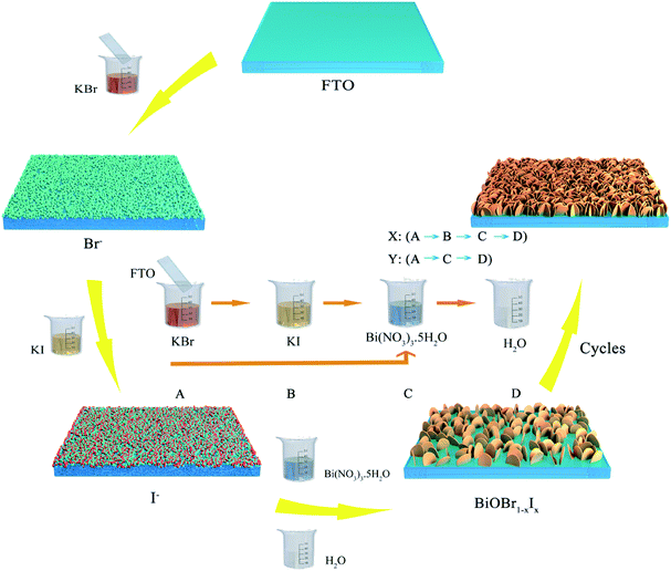 |
| | Fig. 1 Schematic for the preparation of BiOBr1−xIx films by the SILAR process. | |
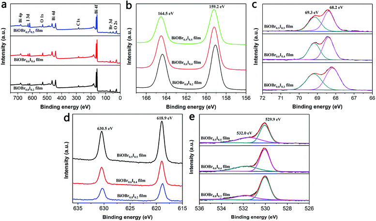 |
| | Fig. 2 The XPS spectra of BiOBr1−xIx films (a) survey, (b) Bi 4f, (c) Br 3d, (d) I 3d, (e) O 1s. | |
Table 1 Atomic concentration table of as-prepared BiOBr1−xIx films
| Samples |
Br 3d |
I 3d |
BiOBr1−xIx |
| BRI-1 |
3.67 |
3.67 |
BiOBr0.5I0.5 |
| BRI-2 |
5.01 |
3.47 |
BiOBr0.6I0.4 |
| BRI-3 |
5.23 |
1.32 |
BiOBr0.8I0.2 |
 |
| | Fig. 3 XRD patterns of BiOBr, BiOBr0.5I0.5, BiOBr0.6I0.4, BiOBr0.8I0.2 and BiOI films. | |
The size and morphology of the as-prepared BiOBr1−xIx films generated by SILAR at room temperature were investigated via field-emission scanning electron microscopy (FESEM), as shown in Fig. 4. Fig. 4a shows that the BiOBr0.8I0.2 film is composed of numerous nanosheets with an individual thickness of approximately 15 to 25 nm. These nanosheets are arranged in a staggered manner, forming a nanosheet array structure vertically on the FTO surface. As x increases in the BiOBr1−xIx films (0.2 to 0.5), the nanosheets in the BiOBr0.5I0.5 film become thicker and denser than those in the BiOBr0.8I0.2 film (Fig. 4a and c). This observation can be attributed to the radii of I− (2.16 Å) being larger than that of Br− (1.95 Å), and the growth of BiOBr1−xIx films may be accelerated by the I− ions. In addition, the composition of the BiOBr0.5I0.5 film was analysed by energy dispersive X-ray spectroscopy (EDS) (Fig. 4d), and the results confirmed the existence of Bi, O, Br and I. To further obtain information on the as-prepared BiOBr1−xIx film on a small scale, two-dimensional (2D) AFM surface height morphologies of BiOBr1−xIx films on FTO substrates were obtained with a scanning area of 2 μm × 2 μm, as shown in Fig. 4e and f.
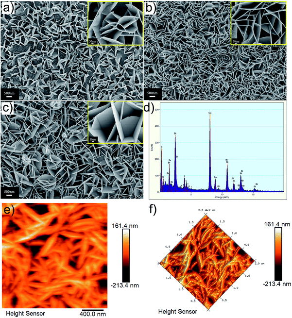 |
| | Fig. 4 SEM images of the as-prepared BiOBr1−xIx films, (a) BiOBr0.8I0.2 film, (b) BiOBr0.6I0.4 film, and (c) BiOBr0.5I0.5 films. (d) EDS pattern, (e and f) AFM height images of BiOBr0.5I0.5 film. | |
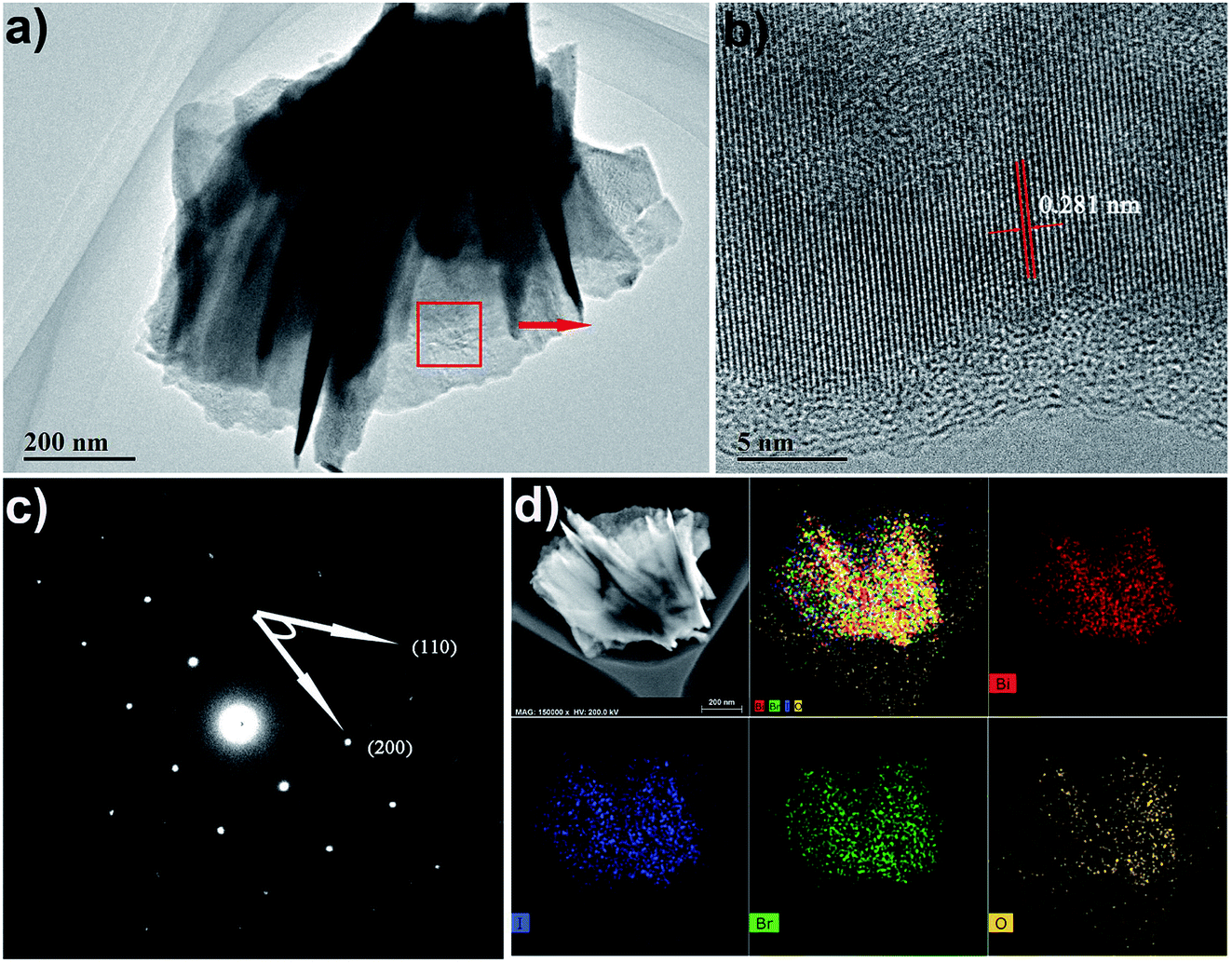
To further investigate the morphology and structure of the BiOBr1−xIx films, TEM and HRTEM analyses were performed. TEM and HRTEM images further proved that the BiOBr0.5I0.5 film obtained at room temperature has high crystallinity, indicating single-crystalline characteristics (Fig. 5a and c). From Fig. 5b, it can be seen that the spacing of the adjacent lattice planes is 0.281 nm, which corresponds well to the (110) facet. It is well known that the distance between the adjacent (110) planes of BiOI is 0.282 nm, and the value for that of BiOBr is 0.278 nm. The above result is consistent with Vegard's law38 and indicates that the I− ion has been successfully inserted into the crystal lattice of BiOBr and replaced the Br− ion. As depicted in Fig. 5c, the corresponding SAED pattern exhibits a clear spot pattern, indicating the excellent single-crystalline character of BiOBr0.5I0.5. The angle between adjacent spots labelled in the SAED pattern is 45°, which is identical to the theoretical value of the angle between the (110) and (200) planes of tetragonal BiOBr0.5I0.5. This means that the set of diffraction spots can be indexed as the [001] zone axis. The elemental composition and distribution of the BiOBr0.5I0.5 nanosheet films were detected by EDS mapping of elements. As shown in Fig. 5d, the EDS mapping of BiOBr0.5I0.5 nanosheets shows that Bi, O, Br, and I elements are homogeneously distributed in the BiOBr0.5I0.5 nanosheets. This indicates that I was homogeneously doped in the BiOBr0.5I0.5 sample.
 |
| | Fig. 5 (a) TEM image, (b) HRTEM image, (c) SAED pattern and (d) EDS mapping images of the as-prepared BiOBr0.5I0.5 nanosheets. | |
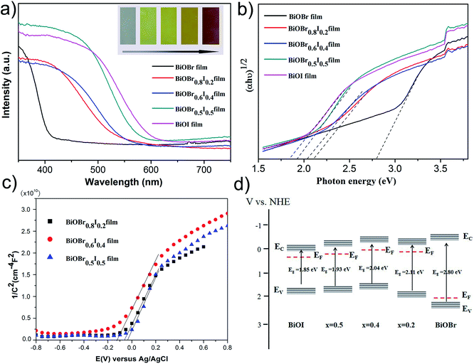
The UV-vis diffuse reflectance spectra (DRS) of the as-prepared films are shown in Fig. 6a. It is found that the optical absorption edges have a clear redshift with increasing iodine content (x from 0.2 to 0.5). Accordingly, the colour of the samples varies gradually from white to brick red. The corresponding maximum absorption wavelength of the pure BiOBr film is 410 nm. The absorption band edge of the BiOBr0.5I0.5 film was broadened compared to that of pure BiOBr to 596 nm due to the significant doping effect of I− ions. The as-prepared BiOBr1−xIx films show strong absorption in the visible light region, illustrating the practicability of the utilization of visible light. It is well known that the relationship between the band edge and optical absorption of a crystalline semiconductor follows the equation:39
where
α,
hν,
A and
Eg represent the optical absorption coefficient, photon energy, proportionality constant and bandgap, respectively. For BiOBr
1−xI
x films, the value of
n is 4 for an indirect bandgap semiconductor.
40 Therefore, the bandgap energy could be estimated from a plot of (
αhν)
1/2 versus photon energy (
hν), which is given in
Fig. 6b. The bandgap energies of the BiOBr, BiOBr
0.8I
0.2, BiOBr
0.6I
0.4, BiOBr
0.5I
0.5 and BiOI films are 2.80, 2.11, 2.04, 1.93 and 1.85 eV, respectively. It can be deduced that the bandgap energies and band structures for BiOBr
1−xI
x films can be tuned by controlling the molar ratio of bromine and iodine.
 |
| | Fig. 6 (a) UV-vis DRS spectra (inset image is photograph), (b) energy gap calculated by plotting (αhν)1/2 versus hν, (c) Mott–Schottky plots and (d) band structures of BiOBr, BiOBr1−xIx and BiOI films. | |
To confirm the type of semiconductor and flat-band potentials of the BiOBr1−xIx films, Mott–Schottky (M–S) curves of the as-prepared films were produced, as shown in Fig. 6c. According to the positive slopes of the straight lines found in the measured plots, the BiOBr0.8I0.2, BiOBr0.6I0.4 and BiOBr0.5I0.5 films were identified as n-type semiconductors.30,41 The flat-band potential (Vfb) was determined by the equation:8
| |
 | (2) |
here,
ε0,
εr,
NA and
V represent the permittivity in vacuum, relative permittivity, carrier density and applied potential, respectively.
kB is the Boltzmann constant,
T is the absolute temperature, and
e corresponds to the electronic charge. Hence, a plot of 1/
C2 vs. potential (
V) will yield a line that, when extrapolated to the
x-axis, corresponds to the flat-band potential of the semiconductor.
9,41 The flat-band position (
Vfb) values of the BiOBr
0.8I
0.2, BiOBr
0.6I
0.4 and BiOBr
0.5I
0.5 films were thus calculated to be −0.06, −0.12 and −0.03 V
vs. the Ag/AgCl electrode, equivalent to 0.15, 0.09 and 0.18 V
vs. the normal hydrogen electrode (NHE), respectively.
17 Based on the results of the Mott–Schottky plots and UV-vis DRS spectra, a schematic diagram of the band structures for BiOBr, BiOI, BiOBr
0.8I
0.2, BiOBr
0.6I
0.4 and BiOBr
0.5I
0.5 films is drawn in
Fig. 6d. Interestingly, the BiOBr film exhibits a predominant location of the conduction band (CB) and valence band (VB) due to its wide bandgap. In addition, both the CB and VB positions of BRI-1, BRI-2 and BRI-3 significantly shift up with the decrease in the I/Br molar ratio compared to the CB and VB positions of the BiOI film.
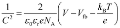
To reveal the effective transfer of photoelectrons intuitively, time-resolved photoluminescence (TRPL) decay spectra were obtained. As clearly seen from Fig. 7a, all of the TRPL spectra display a monoexponential decay process. In addition, their decay dynamics can be obtained through fitting to a monoexponential function:42
| |
I = I0![[thin space (1/6-em)]](https://www.rsc.org/images/entities/char_2009.gif) exp(−t/τ) exp(−t/τ)
| (3) |
where
I0 is the PL intensity and
τ is the corresponding lifetime. The fitted TRPL spectra indicate that the average lifetimes of the carriers (
τavg) are 1.22, 1.11 and 1.08 ns for the BiOBr
0.5I
0.5, BiOBr
0.6I
0.4 and BiOBr
0.8I
0.2 films, respectively. The increased
τavg of the BiOBr
0.5I
0.5 film implies that the existence of shallow surface states could prolong the photogenerated charge lifetime.
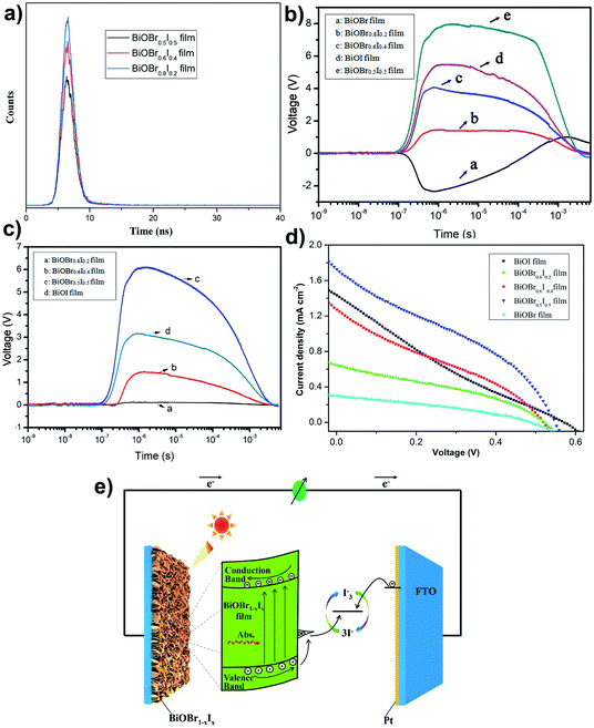 |
| | Fig. 7 (a) TRPL spectra, TPV spectra of BiOBr, BiOBr1−xIx and BiOI films with front side illumination by 355 nm laser (b) and 532 nm laser (c), respectively. (d) I–V curves of based-on BiOBr, BiOBr1−xIx and BiOI solar cells. (e) Schematic illustration of photogenerated charge transfer in the BiOBr1−xIx based-on solar cells. | |
Transient photovoltaic (TPV) measurements were carried out to reveal the kinetics of photoinduced charge carrier separation and transfer at the surface and interface. Fig. 7b and c shows the TPV spectra of BiOBr1−xIx films under front illumination by 355 nm and 532 nm laser pulses, respectively. For a single BiOBr film, a negative photovoltage implies that photoinduced electrons accumulate on the surface, driven by a surface electric field directed from the surface to the interior of BiOBr. However, the TPV signals of the BiOBr1−xIx and BiOI films are positive, indicating accumulation of photoinduced holes on the surface. According to the TPV results (Fig. 7b and c), the TPV signal of the BiOBr1−xIx film is stronger with increasing iodine doping amount, and the BiOBr0.5I0.5 film has the strongest TPV signal under irradiation with 355 nm or 532 nm laser pulses. However, the single BiOBr film cannot be excited by the 532 nm laser to generate a surface photovoltage signal (Fig. 7c). The photoinduced carrier concentration reached its maximum at 7.5 × 10⁻⁷ s on the surface of the BiOBr0.5I0.5 film under 355 nm light illumination as a result of the drift of photogenerated carriers under an electric field. Moreover, recombination of photo-generated electrons and holes occurred at 5.0 × 10⁻⁴ s, and the recombination time of 4.8 × 10⁻³ s for the BiOBr0.5I0.5 film was slower than that of the other BiOBr1−xIx films. Fig. 7d shows the current density–voltage (J–V) characteristic curves of the solar cells under illumination (simulated AM 1.5 sunlight), and the main photovoltaic parameters are listed in Table 2. On the basis of these results, a single BiOBr film electrode has a relatively poor photovoltaic performance. However, the BiOBr1−xIx-based solar cells showed a marked increase in the conversion of light to electric current compared with the single BiOBr-based or BiOI-based solar cells. The BiOBr0.5I0.5-based solar cell can achieve the highest short-circuit current of 1.73 mA cm−2, an open-circuit voltage of 0.55 V, a PCE (η) of 0.53, and a fill factor (FF) of 0.34. The improved photovoltaic performance was attributed to the effective light absorbance and sufficient charge separation in the BiOBr0.5I0.5 film. Fig. 7e gives a charge transfer mechanism in the solar cell, different from that in traditional TiO2-based dye sensitized solar cells (DSSCs). First, the incident photons are absorbed by the BiOBr1−xIx film, and electron–hole pairs are generated. The photogenerated electrons transfer to the conduction band and move to the FTO substrate. Meanwhile, the holes are trapped by the donor surface state formed by iodine doping, and the localized holes can react with the electrons in the electrolyte. Based on the above inference, it is easily demonstrated that iodine doping in BiOBr film is beneficial to the separation and transmission of photogenerated charge carriers and improves the photoelectric conversion performance.
Table 2 Summary of device performance for the cells based on the BiOBr, BiOBr1−xIx and BiOI solar cells
| Samples |
Voc (V) |
Jsc (mA cm−2) |
FF (%) |
η (%) |
| BiOBr |
0.49 |
0.30 |
32.3 |
0.079 |
| BiOBr0.8I0.2 |
0.52 |
0.65 |
35.0 |
0.20 |
| BiOBr0.6I0.4 |
0.52 |
1.28 |
28.7 |
0.32 |
| BiOBr0.5I0.5 |
0.55 |
1.73 |
33.7 |
0.53 |
| BiOI |
0.57 |
1.44 |
19.8 |
0.27 |
Conclusion
In summary, I-doped BiOBr1−xIx (x = 0.2, 0.4, 0.5) nanosheet array films with perfect single-crystal structures were prepared by a simple and low-energy SILAR method at room temperature for the first time. The as-obtained BiOBr1−xIx films were constructed by numerous nanosheets, which exhibited a thickness of 15–25 nm. The modification of the energy band structure for the BiOBr1−xIx films was determined, and the bandgap could be tuned from 2.80 to 1.85 eV by varying the Br/I molar ratio. The Mott–Schottky curves and surface photovoltage results demonstrate that the BiOBr1−xIx films have the characteristics of an n-type conductor, indicating that the doping of I− ions changes the conductivity type of the p-type BiOBr film semiconductor. Due to the existence of a donor surface state formed by iodine doping, the BiOBr0.5I0.5 film has a long photogenerated charge lifetime, a better and wider surface photovoltage response and significantly improved photoelectric conversion performance. In recent years, we have constructed a series of bismuth oxyhalide films at room temperature and systematically studied the separation and transfer behaviour of photoinduced electron–hole pairs in bismuth oxyhalide films. Our study provides a new idea for the design and synthesis of bismuth oxyhalide photoelectric films and new insights into the photoelectric mechanisms of bismuth oxyhalide heterostructures.
Experimental section
Materials
All of the reagents used for preparing the samples were of analytical grade, obtained from Sinopharm Chemical Reagent Co., Ltd. (Shanghai, China) and used without further purification. Fluorine-doped tin oxide (FTO) glass was purchased from Nippon Sheet Glass Co., Ltd. Deionized (DI) water was used in all experiments.
Synthesis of BiOBr1−xIx films
BiOBr1−xIx nanosheet films were deposited directly onto FTO substrates through a modified successive ionic layer adsorption and reaction (SILAR) method. In a typical experiment, 5 mmol KBr, 5 mmol KI and 5 mmol Bi(NO3)3·5H2O were dissolved in 40 mL deionized water under continuous stirring at room temperature, respectively. In each cycle, the pretreated FTO substrates were successively immersed into the KBr and KI solutions for 10 s to absorb Br− and I− ions. Subsequently, the FTO substrates were impregnated by the Bi(NO3)3 solution for 10 s to generate BiOBr1−xIx nanosheets on the FTO through reaction with Bi3+ ions, followed by rinsing with deionized water. The above single SILAR cycle was denoted one X cycle. After thirty X cycles, the obtained films were vacuum-dried at 60 °C for 2 h. The resulting BiOBr1−xIx film sample was denoted BRI-1. To obtain BiOBr1−xIx film samples with different atomic ratios of bromine and iodine, the following parallel experiments were carried out. (1) In odd number cycles, the FTO substrate was successively immersed into the KBr, KI and Bi(NO3)3 solutions for 10 s. Then, the substrate was rinsed with deionized water to remove excess ions. One X cycle was completed. Subsequently, the above resulting FTO substrate was immersed only into the KBr and Bi(NO3)3 solutions for 10 s in even number cycles, in which one Y cycle was performed. After fifteen (XY) cycles, the obtained BiOBr1−xIx film samples were vacuum-dried at 60 °C and denoted BRI-2. (2) The FTO substrate was immersed into the KBr, KI and Bi(NO3)3 solutions for one X cycle. In the second and third cycles, the resulting FTO substrate was only immersed into the KBr and Bi(NO3)3 solutions for two Y cycles. After ten (XYY) cycles, the obtained BiOBr1−xIx film samples were vacuum-dried at 60 °C and denoted BRI-3. A schematic for the preparation of BiOBr1−xIx films by the SILAR process is depicted in Fig. 1.
Characterization
The morphologies and microstructures of the resulting thin films were characterized by field-emission scanning electron microscopy (FESEM, S-4800) and field-emission transmission electron microscopy (FETEM, JEM-2100F). Prior to TEM analysis, the samples were scraped from the films on the FTO substrates, dispersed in ethanol using an ultrasonication process, and deposited onto carbon-copper grids. Energy dispersive X-ray spectroscopy (EDS) images and selected area electron diffraction (SAED) patterns were measured using a JEM-2100F. The purity and crystallinity of the as-prepared films were recorded by X-ray diffraction (XRD, Bruker D8 Advance diffractometer) with nickel-filtered CuKα radiation (λ = 1.5418 Å). The UV-vis absorption spectra of the as-prepared films were recorded on a Varian Cary 5000 UV-vis-NIR spectrophotometer. X-ray photoelectron spectroscopy (XPS) was employed to analyse the chemical composition and atomic valence states of the samples (XPS, Thermo Scientific Escalab 250 Xi). In the experiments, Al Kα was used as the excitation source, with CIs = 284.6 eV as the energy reference. Time-resolved PL (TRPL) decay spectra were obtained on an FLS 920 fluorescence spectrometer (Edinburgh).
Photoelectrochemical measurements
The Mott–Schottky curves were evaluated using an electrochemical system (CHI-760E) in a three-electrode assembly with 0.5 M Na2SO4 (pH = 5.8) as the electrolyte. A Pt plate and a Ag/AgCl electrode were used as the counter and reference electrodes, respectively. The Mott–Schottky measurements were recorded using an AC voltage amplitude of 5 mV and a frequency of 1 kHz. Time-resolved photovoltage (TPV) measurements were carried out with the device described in our previous paper.32 The sandwich-like structure was constructed using the sample, mica, and ITO substrate for all TPV tests. The samples were excited with different laser radiation pulses (wavelengths of 355 nm and 532 nm, pulse width of 4 ns) from a third harmonic Nd:YAG laser (Quantel Brilliant Eazy: BRILEZ/IR-10). The transient surface photovoltage data were recorded using a 500 MHz digital oscilloscope (TDS 3054C, Tektronix). The J–V curves of solar cell devices based on BiOBr1−xIx (using as-prepared samples as the working electrode, sputtered Pt/FTO as the counter electrode and a redox electrolyte composed of 0.05 M I2, 0.5 M LiI, 0.3 M DMPII and 0.5 M 4-TBP in 3-methoxy acrylonitrile) were measured using a Keithley 2400 source meter under simulated solar light illumination (Newport 91192STS simulator equipped with an AM 1.5 G filter).
Conflicts of interest
The authors declare no competing financial interest.
Acknowledgements
This work is supported financially by the National Natural Science Foundation of China (51772256), the Program for Innovative Research Team (in Science and Technology) in University of Henan Province (19IRTSTHN026), the Zhongyuan Thousand Talents Project of Henan Province (204200510016).
Notes and references
- Y. Huo, J. Zhang, M. Miao and Y. Jin, Appl. Catal., B, 2012, 111–112, 334–341 CrossRef CAS.
- H. Liu, Y. Su, Z. Chen, Z. Jin and Y. Wang, J. Hazard. Mater., 2014, 266, 75–83 CrossRef CAS.
- J. Y. Xia, S. Yin, H. M. Li, H. Xu, Y. S. Yan and Q. Zhang, Langmuir, 2011, 17, 1200–1206 CrossRef.
- T. Li, X. C. Zhang, C. M. Zhang, R. Li, J. X. Liu, R. Lv, H. Zhang, P. D. Han, C. M. Fan and Z. F. Zheng, Phys. Chem. Chem. Phys., 2019, 21, 868–875 RSC.
- L. Chen, C. T. Yang and C. Y. Yan, J. Mater. Sci. Technol., 2020, 48, 100–104 CrossRef.
- J. Li, Y. Yu and L. Zhang, Nanoscale, 2014, 6, 8473–8488 RSC.
- M. Guan, C. Xiao, J. Zhang, S. J. Fan, R. An, Q. M. Cheng, J. F. Xie, M. Zhou, B. J. Ye and Y. Xie, J. Am. Chem. Soc., 2013, 135, 10411–10417 CrossRef CAS.
- L. S. Gómez-Velázquez, A. Hernández-Gordillo, M. J. Robinson, V. J. Leppert, S. E. Rodil and M. Bizarro, Dalton Trans., 2018, 47, 12459–12467 RSC.
- D. S. Bhachu, S. J. A. Moniz, S. Sathasivam, D. O. Scanlon, A. Walsh, S. M. Bawaked, M. Mokhtar, A. Y. Obaid, I. P. Parkin, J. W. Tang and C. J. Carmalt, Chem. Sci., 2016, 7, 4832–4841 RSC.
- A. M. Ganose, M. Cuff, K. T. Butler, A. Walsh and D. O. Scanlon, Chem. Mater., 2016, 28, 1980–1984 CrossRef CAS.
- J. Li, L. Z. Zhang and Y. J. Li, Nanoscale, 2014, 6, 167–171 RSC.
- C. J. Huang, J. L. Hu, S. Cong, Z. G. Zhao and X. Q. Qiu, Appl. Catal., B, 2015, 174–175, 105–112 CrossRef CAS.
- S. M. Wang, Y. Guan, L. P. Wang, W. Zhao, H. He, J. Xiao, S. G. Yang and C. Sun, Appl. Catal., B, 2015, 168–169, 448–457 CrossRef CAS.
- G. Hani and S. Yoel, ACS Catal., 2013, 3, 186–191 CrossRef.
- J. Xiong, Q. Dong, T. Wang, Z. Jiao, G. Lu and Y. Bi, RSC Adv., 2014, 4, 583–586 RSC.
- Y. C. Yu, C. J. Li, S. S. Huang, Z. J. Hu, Z. W. Chen and H. W. Gao, RSC Adv., 2018, 8, 32368–32376 RSC.
- Y. L. Ling and Y. Z. Dai, Appl. Surf. Sci., 2020, 509, 145201–145213 CrossRef CAS.
- X. Lou, J. Shang, L. Wang, H. F. Feng, W. C. Hao, T. M. Wang and Y. Du, J. Mater. Sci. Technol., 2017, 33, 281–284 CrossRef.
- Y. G. Xu, H. Xu, J. Yan, H. M. Li, L. Y. Huang, Q. Zhang, C. J. Huang and H. L. Wan, Phys. Chem. Chem. Phys., 2013, 15, 5821–5830 RSC.
- C. L. Yu, F. F. Cao, G. Li, R. F. Wei, J. C. Yu, R. C. Jin, Q. Z. Fan and C. Y. Wang, Sep. Purif. Technol., 2013, 120, 110–122 CrossRef CAS.
- Y. Huang, B. Long, H. Li, M. S. Balogun, Z. Rui, Y. Tong and H. Ji, Adv. Mater. Interfaces, 2015, 2, 1500249 CrossRef.
- L. Cai, G. Q. Zhang, Y. F. Zhang and Y. Wei, CrystEngComm, 2018, 20, 3647–3656 RSC.
- H. Gnayem and Y. Sasson, J. Phys. Chem. C, 2015, 119, 19201–19209 CrossRef CAS.
- M. B. Hussain, M. S. Khan, H. M. Loussala and M. S. Bashir, RSC Adv., 2020, 10, 4763–4771 RSC.
- L. F. Qi, Y. W. Yang, P. X. Zhang, Y. Le, C. Wang and T. Wu, Appl. Surf. Sci., 2019, 467–468, 792–801 CrossRef CAS.
- G. Liu, T. Wang, S. Ouyang, L. Liu, H. Jiang, Q. Yu, T. Kako and J. Ye, J. Mater. Chem. A, 2015, 3, 8123–8132 RSC.
- Z. Jia, F. Wang, F. Xin and B. Zhang, Ind. Eng. Chem. Res., 2011, 50, 6688–6694 CrossRef CAS.
- K. Ren, J. Liu, J. Liang, K. Zhang, X. Zheng, H. Luo, Y. Huang, P. Liu and X. Yu, Dalton Trans., 2013, 42, 9706–9712 RSC.
- C. Bi, J. Cao, H. Lin, Y. Wang and S. Chen, RSC Adv., 2016, 6, 15525–15534 RSC.
- H. M. Jia, W. W. He, B. B. Zhang, L. Yao, X. K. Yang and Z. Zheng, Appl. Surf. Sci., 2018, 441, 832–840 CrossRef CAS.
- N. T. Hahn, S. Hoang, J. L. Self and C. B. Mullins, ACS Nano, 2012, 6, 7712–7722 CrossRef CAS.
- H. M. Jia, B. B. Zhang, W. W. He, Y. Xiang and Z. Zheng, Nanoscale, 2017, 9, 3180–3187 RSC.
- J. Y. Liu, Y. Bai, P. Y. Luo and P. Q. Wang, Catal. Commun., 2013, 42, 58–61 CrossRef CAS.
- H. Liu, W. R. Cao, Y. Su, Y. Wang and X. H. Wang, Appl. Catal., B, 2012, 111–112, 271–279 CrossRef CAS.
- J. J. Hu, G. Q. Xu, J. W. Wang, J. Lv, X. Y. Zhang, Z. X. Zheng, T. Xie and Y. C. Wu, New J. Chem., 2014, 38, 4913–4921 RSC.
- G. Cheng, J. Y. Xiong and F. J. Stadler, New J. Chem., 2013, 37, 3207–3213 RSC.
- C. R. Zheng, C. B. Cao and Z. Ali, Phys. Chem. Chem. Phys., 2015, 17, 13347–13354 RSC.
- S. S. Khalil, V. Uvarov and Y. L. Kritsman, Catal. Commun., 2011, 12, 1136–1141 CrossRef.
- Y. Peng, J. Xu, T. Liu and Y. G. Mao, CrystEngComm, 2017, 19, 6473–6480 RSC.
- L. Cai, G. Q. Zhang, Y. F. Zhang and Y. Wei, CrystEngComm, 2018, 20, 3647–3656 RSC.
- Y. Zhang, Q. Pei, J. C. Liang, T. Feng, X. Zhou, H. Mao, W. Zhang, Y. Hisaeda and X. M. Song, Langmuir, 2015, 3, 10279–10284 CrossRef.
- L. Zhang, C. G. Niu, X. F. Zhao, C. Liang, H. Guo and G. M. Zeng, ACS Appl. Mater. Interfaces, 2018, 10, 39723–39734 CrossRef CAS.
|
| This journal is © The Royal Society of Chemistry 2020 |
Click here to see how this site uses Cookies. View our privacy policy here. 
 Open Access Article
 This Open Access Article is licensed under a Creative Commons Attribution-Non Commercial 3.0 Unported Licence
 *,
Yuxing Li,
Yuanyang Mao,
Dufei Yu,
Weiwei He
*,
Yuxing Li,
Yuanyang Mao,
Dufei Yu,
Weiwei He