
 Open Access Article
 This Open Access Article is licensed under a Creative Commons Attribution-Non Commercial 3.0 Unported Licence
Multilevel storage and photoinduced-reset memory by an inorganic perovskite quantum-dot/polystyrene floating-gate organic transistor†
Risheng Jina,
Jin Wang b,
Keli Shi*a,
Beibei Qiua,
Lanchao Mac,
Shihua Huang*a and
Zhengquan Li*b
b,
Keli Shi*a,
Beibei Qiua,
Lanchao Mac,
Shihua Huang*a and
Zhengquan Li*b
aCollege of Physics and Electronic Information Engineering, Zhejiang Normal University, Jinhua, Zhejiang 321004, P. R. China. E-mail: shikl@zjnu.edu.cn; huangshihua@zjnu.cn
bKey Laboratory of the Ministry of Education for Advanced Catalysis Materials, Zhejiang Normal University, Jinhua, Zhejiang 321004, P. R. China. E-mail: zqli@zjnu.edu.cn
cCollege of Materials Science and Engineering, Beijing Key Laboratory of Special Elastomer Composite Materials, Beijing Institute of Petrochemical Technology, Beijing 102617, P. R. China
First published on 27th November 2020
Abstract
Inorganic halide perovskite quantum dots (IHP QDs) have been widely studied in optoelectronic devices because of their size-dependent tunable bandgaps, long electron–hole diffusion lengths and excellent absorption properties. Herein, a novel floating-gate organic field-effect transistor memory (FGOFETM) is demonstrated, comprising a floating-gate of IHP QDs embedded in a polystyrene matrix. Notably, the FGOFETM exhibits photoinduced-reset characteristic that allows data removal by photo irradiation. This feature makes low energy-consuming memory and innovative devices possible. The nonvolatile devices also show a large memory window (≈90 V), ultrahigh memory on/off ratio (over 107) and therefore excellent multilevel information storage, in which 4 recognizable non-volatile states and long retention time (up to 10 years) are obtained. This work not only offers an effective guideline of high-performance FGOFETMs, but also shows great potential to realize multilevel data storage under electrical programming and photoinduced-reset processes.
Introduction
In the past two decades, non-volatile memory based on organic field-effect transistors (OFETs) has attracted much attention due to its merits of non-destructive read-out, light weight, easy processing, low fabrication cost and strong compatibility with current integrated circuit process.1–3 Among various types of OFET memory, the floating-gate OFET memory (FGOFETM) is considered as a candidate for the next generation organic flash memory due to tunable floating-gate for device sizing, low temperature solution-processability, fast data storage and viabilities of device fabrication on flexible substrates.4,5 Compared to traditional floating gate, the composite film, monodispersed nanoparticles (NPs) or quantum dots (QDs) impregnated in a dielectric polymer, as a floating gate layer has following advantages:6–8 (1) the floating gate layer can be prepared by a simple and highly effective solution process method; (2) the morphology and nano-floating gate structure can be controlled by adjusting the mixing ratio of nanoparticles materials and polymers, therefore improving the OFET memory performance; (3) the memory devices have higher film uniformity and lower gate leakage. In addition, it also has better size scalability, higher data storage density and prevention of lateral charge movement.9 Owing to the above advantages, the FGOFETMs based on NPs or QDs/polymer composite film can obtain large memory window, high memory on/off ratio and enhanced memory data retention, which is suitable for practical multilevel storage.10 It is challenging but rewarding to realize multilevel organic memory due to: (1) internet of things (IoT), the demand for information storage is ever-increasing to meet the demands of artificial intelligence and machine learning; (2) Moore's law approaches the physical limit, thus it is urgent to further increase storage density for larger memory space;3,11 (3) the size of memory device is limited by the precision of the photolithography process, which makes it difficult to further reduce the size of each memory cell. Currently, it is a hot topic to explore the use of multilevel memory devices instead of single-level memory devices to achieve high-density data storage performance.3,8,12–15 However, the capability of storing multilevel information is one of the biggest challenges in memory technologies.5,10,11,15–17 Thus, there is an urgent demand to search for suitable NPs/QDs and organic semiconductor (OSC) channel materials for highly efficient, multilevel and endurable OFET memory devices.Recently, all-inorganic halide perovskite quantum dots (IHP QDs) have been widely applied in the fields of photovoltaics, photodetectors and non-volatile memories owing to their fascinating properties including narrow emission bandwidths, excellent absorption properties, long charge carrier lifetime and colossal ferroelectricity.18–20 It has been believed that the IHP QDs could be an excellent candidate as the nano-floating gate to fabricate high-performance FGOFETMs. In addition, due to the excellent optical properties of IHP QDs, the IHP QDs based FGOFETMs have the optical memory characteristics.21 According to photo illumination's role in device operations, the optical-related OFET memory can be divided into photo-programming/electrical erasing and electrical programming/photo-erasing OFET-type memories.21–23 At present, progress in the IHP QDs based FGOFETMs is mainly limited to the former genre.21 Nevertheless, recently, electrical programming/photo-erasing OFET memories with photoinduced-reset characteristic are of great interest, because they offer a novel strategy for information acquisition in the field of OFET optical memories.24–27 For example, Liao and co-workers reported the 2D perovskite-based transistor-type photomemory using a 2D Cs2Pb(SCN)2Br2/polymer hybrid film as the floating gate.27 Compared to the conventional OFET-type memories modulated only by electrical bias, optical memories with “photoinduced-reset” behavior can be erased by light-only bias that completely replace electrical stress to act as a charge erasing method to realize the memory behaviors of the OFET-type memories. It can not only conveniently eliminate the stored charges and energy savings (bias-free erasing), but also extend application as a memory-related photosensor.24–26 In addition, benefiting from the integration of photodetection and charge storage functions, the memory can possess remarkable advantages of excellent charge storage ability, data protection capability and the utilization of green energy in a single device.21,28,29 Thus, the rapid development of optical memories is extremely significant to the further development of their practical application.1,16,25 Based on our knowledge, there are limited reports to study both the photoinduced-reset characteristic and multilevel storage of FGOFETMs based on IHP QDs/polymer composite film as floating gates. Furthermore, at present, there are two possible operation principles explaining the “photoinduced reset”.26 The first operation principle: photoexcitons are generated initially in organic semiconductor layer under light. The second operation principle: quantum dots or nanoparticles embedded in polymer are excited. Therefore, the mechanism of photoinduced-reset memory devices based on IHP QDs/polymer is ambiguous and detailed studies on the mechanism of the photoinduced-reset process are urgently needed.
In this work, a non-volatile transistor memory with both multilevel storage and photoinduced-reset is demonstrated, in which a floating-gate comprising polystyrene (PS) matrix impregnated with CsPbBr3 (CPB) QDs is employed. CPB QDs are chosen owing to the high charge carrier mobility, outstanding thermal stability, good absorption properties and excellent charge storage property.19,21 In addition to floating-gate materials, the organic semiconductor channel materials are also crucial for high performance FGOFETMs. Among a variety of organic semiconductors, pentacene and C8-BTBT are chosen as proper materials to fabricate our FGOFETMs because of well-matched energy band with CPB QDs, high hole mobility, high Ion/Ioff ratio, ultralow off-current and good stability in air.30,31 The majority of the reported high performance FGOFETMs were fabricated with C8-BTBT or pentacene as the active layers due to their advantages.21,24,26,32 As a result, our non-volatile devices exhibit eminent overall memory performance, including a large memory window (≈90 V), ultrahigh memory on/off ratio (over 107), excellent multilevel storage and good reliability with the retention time over 10 years. Furthermore, the FGOFETM shows photoinduced-reset characteristic, which leads to lower energy consumption erasing operation. At last, we further investigated the mechanism of photoinduced-reset memory devices and proposed the guideline for such photoinduced-reset and multilevel memory devices.
Experimental section
Materials
Polystyrene (PS, Mw = 280![[thin space (1/6-em)]](https://www.rsc.org/images/entities/char_2009.gif) 000, 99%), C8-BTBT (99%), pentacene (99.995%), PbBr2 (99.999%), octadecene (ODE, 99.8%), oleic acid (OA, 90%), oleylamine (OAm, 70%), and Cs2CO3 (99.9%) were purchased from Sigma Aldrich. Hexane, ethyl acetate (EA) and toluene were purchased from Aladdin. Heavily n-doped silicon wafers with 300 nm thick SiO2 dielectric layer were used as substrates. All regents were commercially available and used without further purification.
000, 99%), C8-BTBT (99%), pentacene (99.995%), PbBr2 (99.999%), octadecene (ODE, 99.8%), oleic acid (OA, 90%), oleylamine (OAm, 70%), and Cs2CO3 (99.9%) were purchased from Sigma Aldrich. Hexane, ethyl acetate (EA) and toluene were purchased from Aladdin. Heavily n-doped silicon wafers with 300 nm thick SiO2 dielectric layer were used as substrates. All regents were commercially available and used without further purification.
Synthesis of CsPbBr3 QDs
CsPbBr3 QDs were synthesized according to a literature procedure.33 Briefly, PbBr2 (0.188 mmol) and ODE (5 mL) were added into 3-neck round-bottom flask. The mixture was dried under vacuum at 120 °C for 1 h. Afterwards, OAm (0.5 mL) and OA (0.5 mL) were injected into the PbBr2 precursor at 140 °C under N2. In the meantime, the Cs-oleate solution was prepared by mixing Cs2CO3 (100 mg), OA (0.6 mL) and ODE (4 mL) at 150 °C for 1 h under N2 flow. The temperature was raised to 180 °C after the PbBr2 salt was completely dissolved, and Cs-oleate solution (0.5 mL, 0.125 M) was rapidly injected. After 5 s, the mixture was cooled by using an ice-water bath. The crude QDs solution was added into 5 mL hexane and was centrifuged at 6000 rpm for 5 minutes to separate the undissolved particles. Subsequently, EA (hexane:EA = 1:1, v/v) was added into the supernatant to obtain CsPbBr3 QDs. The aggregation was centrifuged at 6000 rpm for 5 min. After centrifugation, the supernatant was discarded and the QDs were dried.
Fabrication of the floating-gate memory
The SiO2/Si substrates were ultrasonically cleaned with deionized water, isopropyl alcohol, acetone and alcohol, respectively. After we dried the substrates with pure nitrogen, they were treated with UV-generated O3 flow (UVO) for 15 min. The 1.5 mg mL−1 CPB QDs dissolved in toluene were mixed with 5 mg mL−1 PS into ratios of 1:1, 3:1, 4:1, and 6:1 according to their volumes. The PS and CPB QDs/PS layers were spin-coated (3000 rpm, 60 s) onto the substrates and the samples were annealed at 80 °C for 60 min to remove residual solvent. The pentacene film or C8-BTBT film was then deposited on CPB QDs/PS composite films by vacuum evaporation under a pressure of about 8.0 × 10⁻⁵ Pa. After the pentacene film or C8-BTBT film was deposited, patterned gold source–drain electrodes (80 nm) were deposited by vacuum evaporation. The channel lengths (L) and widths (W) of our FGOFETMs were 40 and 1400 μm, respectively.
Characterization
The electrical properties of all devices were measured with a Keysight B1500A semiconductor characterization system in ambient atmosphere. The UV-visible absorption spectra of C8-BTBT, pentacene and CPB QDs films were characterized by using a PerkinElmer UV-vis lambda 365 spectrophotometer. Transmission electron microscope (TEM) image was recorded with JEOL JEM-2100F TEM. The images of the surfaces were performed through a field emission scanning electron microscope (ZEISS Gemini SEM 300). The morphologies of film surfaces were measured using an atomic force microscopy (VistaScope, Dimension 3100V). The light sources were white, blue (470 nm) and red (630 nm) LEDs. The illumination intensities of lights were measured by visible light-near infrared irradiatometer (400–1000 nm).Results and discussion
The device structure of the bottom-gate top-contact FGOFETM and the chemical structures of pentacene and C8-BTBT are shown in Fig. 1a and b, respectively. The UV-visible absorption spectra of C8-BTBT, pentacene and CPB films on quartz glass are shown in Fig. 1c and d. The pentacene film exhibits absorption in the wavelength range of 500–700 nm. The absorption spectra of CPB QDs and C8-BTBT films show obvious absorption peaks at wavelength of 400–500 nm and in the UV region, respectively. Fig. 1e shows the TEM image of CPB QDs. We prepared CPB QDs/PS composite films with different volume ratios (CPB QDs:PS = 1:1, 3:1, 4:1 and 6:1). The surface morphologies of CPB QDs/PS composite films were investigated by scanning electron microscope (SEM) in Fig. S1a–d.†
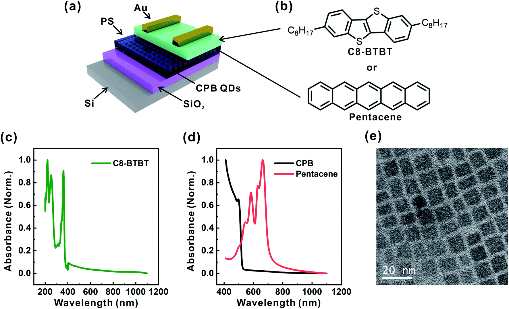 | ||
| Fig. 1 (a) The schematic diagram of the FGOFETMs based on CPB QDs/PS composite film. (b) The molecular structures of pentacene and C8-BTBT. UV-vis spectra of (c) C8-BTBT film, (d) pentacene and CPB films. (e) The TEM image of CPB QDs. | ||
In order to evaluate the memory characteristics of FGOFETMs, the transfer characteristics of devices based on pentacene with different ratios of CPB QDs/PS composite films (CPB QDs:PS = 1:1, 3:1, 4:1 and 6:1) were measured and then illustrated in Fig. 2a–d. The drain voltage (VD) was fixed at −40 V and the gate bias (VG) was changed from 60 V to −100 V. After the applying of VG = −200 V for only 10 ms, the transfer curves of these FGOFETMs all exhibit remarkable shifts to the negative direction, while the device with pure PS film just displays quite negligible shift, as shown in Fig. S2.† The negative gate voltage applied results in the capture of holes in CPB QDs, which is hole-trapping mode, and the stored positive charges further hinder the formation of hole channels.22,24 Interestingly, when positive gate voltage was applied, that is traditional electrical erasing operation, the transfer curve of the programmed devices hardly shifted in Fig. S3.† The reason for this phenomenon may be that the injected holes in the CPB QDs have high stability, resulting in the trapped charges cannot be released by applying the positive gate bias.25 Notably, once the memory devices are exposed to white light with an intensity of 14.4 mW cm−2 for 60 s, the negatively shifted transfer curves recover to the initial state, which shows photoinduced-reset characteristic. The devices based on CPB QDs/PS composites (CPB QDs:PS = 1:1, 3:1, 4:1 and 6:1) exhibit large memory windows (41.27 V, 44.54 V, 42.96 V, and 36.59 V), while the memory window of device without CPB QDs is only 9.11 V, which indicates that the storage capacity of charges is attributed to CPB QDs embedded in the PS. And the above characteristics show that the trapped holes can be completely eliminated only by light illumination, suggesting that light could be utilized as an independent impetus and fulfill the same function as electric stress does. Among them, the device based on CPB QDs/PS composite film (CPB QDs:PS = 3:1) shows the largest memory window (44.54 V). The atomic force microscopy (AFM) topographies of the CPB QDs/PS composite films prepared from various ratios were measured in Fig. S4.† We find that as the ratio of CPB QDs and PS increases, the composite films gradually change from flat surface to mesh-like morphology, which might be CPB QDs aggregation in the PS matrix due to phase segregation. According to the previous research, when the memory layer exists the microphase separation, the corresponding memory device displays a larger memory window.15 In this work, as the ratio of CPB QDs and PS increases from 1:1 to 3:1, the phase separation emerges in the composite film, as shown in Fig. S4.† Therefore, the memory window of the device based on CPB QDs:PS = 3:1 composite film is larger than that of the device based on CPB QDs:PS = 1:1 composite film. On the other hand, for a memory based on a composite film as a floating gate, the storage window is related to the ratio of two components in the composite film. For example, in a previous paper,34 Chen et al. explored the effect of nanoparticle compositions in PMAA on the memory characteristics. When the concentration of the nanoparticles of polyfluorene (PF) increased from 5% to 10%, the memory window increases from 9.47 V to 22.68 V. However, when the concentration increased further, the memory window decreased (concentration = 15%, memory window = 21.22 V; concentration = 20%, memory window = 19.75 V). Similarly, in this work, when the concentration of CPB QDs in the composite film is too large, the memory window decreases. Therefore, the ratios of CPB QDs and PS further increased (from 3:1 to 4:1 and 6:1), that is, the concentration of CPB QDs is too large, exceeding the optimal concentration, the memory window decreased. The AFM images shown in Fig. S5a–d† reveal the surface roughness and morphologies of pentacene films grown on different ratios of CPB QDs/PS composite films (CPB QDs:PS = 1:1, 3:1, 4:1 and 6:1).
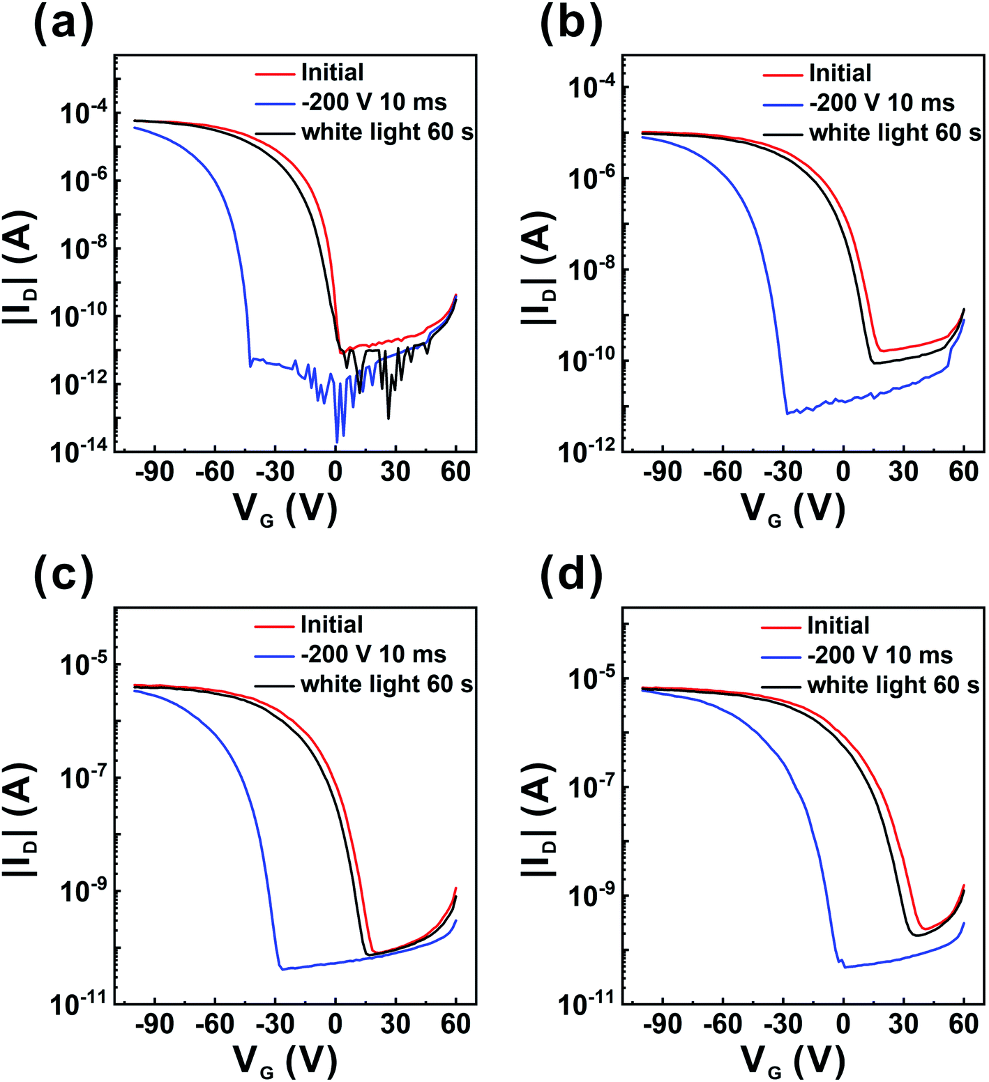 | ||
| Fig. 2 Transfer characteristics (VD = −40 V) of the FGOFETMs based on pentacene with CPB QDs/PS composite floating-gate layers. (a) CPB QDs/PS = 1:1, (b) CPB QDs/PS = 3:1, (c) CPB QDs/PS = 4:1, (d) CPB QDs/PS = 6:1. | ||
Furthermore, in order to prove the adaptability of this photoinduced-reset phenomenon, the FGOFETMs based on C8-BTBT, in which the CPB QDs/PS composite film (CPB QDs:PS = 3:1) was used as floating-gate layer, were further prepared. Fig. 3a shows the transfer characteristics (VD = −40 V) of the FGOFETMs. After a negative gate bias of −200 V was applied to the FGOFETMs for 10 ms under dark, the transfer curve shifted toward the negative direction. Similarly, the programmed memory devices also show ignorable shift when a positive gate bias of 200 V was applied (Fig. S6†) and as they were exposed to white light for 60 s, the transfer curve recovered to the initial state. As a result, the memory devices exhibit excellent memory performance with maximum memory window of ≈90 V and ultrahigh memory on/off ratios over 107. And the effect of light intensity on the photo-erasure process is shown in Fig. S7.† The minimal intensity needed to recharge the device is almost 1 mW cm−2. Retention characteristics of the CPB QDs/PS composites based OFET memories are obtained by independently measuring IDS (VG = −60 V, VD = −40 V) at electrical programming and photo-erasing states, as presented in Fig. 3b. It is demonstrated that both current states could be maintained stably over 104 s, suggesting that the electrical programming as well as photoinduced-reset states are very stable.
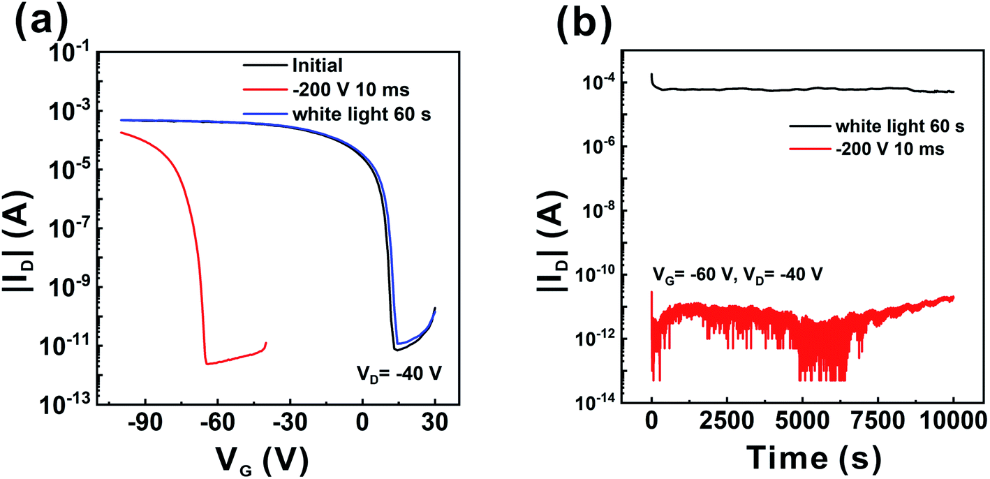 | ||
| Fig. 3 (a) The transfer characteristics and (b) the retention characteristics of the FGOFETMs based on C8-BTBT in electrical programming and photoinduced-reset states. | ||
Due to that the C8-BTBT based FGOFETMs with large memory window and ultrahigh memory on/off ratio (over 107), it has great potential to achieve the multilevel data storage.10,35 Fig. 4a shows the transfer curves of the devices measured after being applied by the various programming voltages of VG, Pro = −50, −100, −120, −140, −160, −180, −200 V (fully programmed state, VD = 0 V, t = 10 ms) and illuminated by white light (fully erased state). The corresponding  versus VG is shown in Fig. 4b. We also observe that the device exhibits controllable levels in the programmed states by varying the program pulse VG input. As shown in Fig. S8,† the ΔVth (memory window) is approximately proportional to the applied gate-voltages. All the phenomena are the prerequisites of realizing multilevel storage in a single device. In addition to adjustable Vth levels and high memory on/off ratios, durability and long retention time are also required to utilize our memory devices as a multilevel non-volatile memory for practical application. First, the cycling tests performed during reduplicative programming/erasing operations are shown in Fig. 4c and d. Consistent and repeatable current level cycles were obtained, indicating the good reliability of the devices. Then, we also measure the retention of the four current states of the FGOFETMs based on C8-BTBT in Fig. 4e. The retention time of 4 current levels are all well maintained even after 10000 s without obvious degradation. Importantly, for our multilevel FGOFETM, highly stable charge storage characteristics in CPB QDs with a quasi-permanent retention time of over 10 years were obtained, as shown in Fig. 4f. Overall, the memory devices based on CPB QDs/PS possess good reliability to stored data for practical applications.36
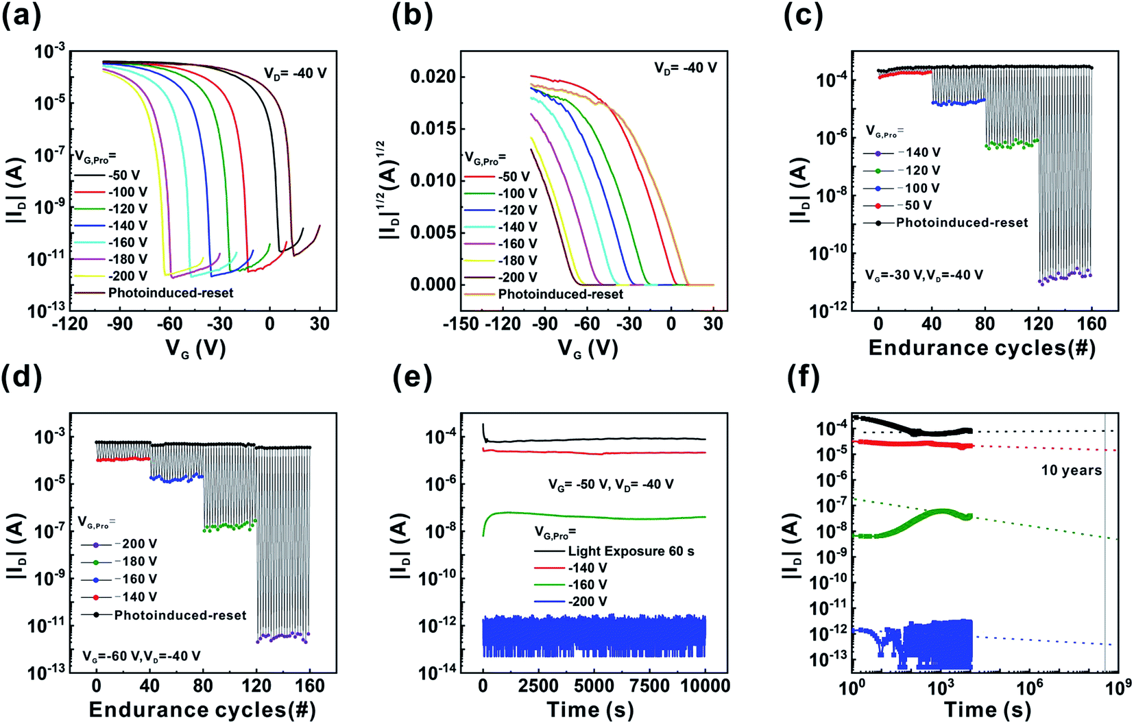 | ||
Fig. 4 (a) I–V characteristics and (b) 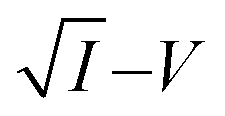 characteristics of the devices based on C8-BTBT with CPB QDs/PS composite floating-gate layer. Program/Erase switching twenty cycles (c) at VG = −30 V, VD = −40 V and (d) at VG = −60 V, VD = −40 V. (e) Retention characteristics of different current levels after programming at VG = −140, −160 and −200 V and photoinduced-reset process. (f) Retention time estimated by the extrapolation of each on- and off-state plot. characteristics of the devices based on C8-BTBT with CPB QDs/PS composite floating-gate layer. Program/Erase switching twenty cycles (c) at VG = −30 V, VD = −40 V and (d) at VG = −60 V, VD = −40 V. (e) Retention characteristics of different current levels after programming at VG = −140, −160 and −200 V and photoinduced-reset process. (f) Retention time estimated by the extrapolation of each on- and off-state plot. | ||
We further investigated the work mechanism of the FGOFETM based on CPB QDs/PS composite film. The corresponding energy band diagrams of CPB QDs/pentacene and CPB QDs/C8-BTBT are shown in Fig. 5a and b, respectively.18,34,37 There are two mechanisms to explain the photoinduced-reset process according to the previous studies, which elaborates that the process is realized through the generation and separation of photoexcitons either in semiconductor layer (Mechanism I) or photoactive charge trapping layer (Mechanism II).26 According to the absorption spectra in Fig. 1d, CPB QDs effectively absorb light at the wavelength region of 400–500 nm, while the maximum absorption peak of C8-BTBT locates at the UV region and it has no absorption in the visible region. However, as shown in Fig. 3a, the programmed memory devices based on C8-BTBT still return to the initial state once being exposed to white light. Thus, for the FGOFETMs based on C8-BTBT, the “photoinduced-reset effect” attributes to the photoresponse of the CPB QDs in the PS matrix under white light (Mechanism II). For the FGOFETMs based on pentacene, both pentacene and CPB QDs have absorption at visible light, it is possible that “photoinduced-reset effect” could attributed to pentacene and CPB QDs simultaneously. In order to further clearly investigate the mechanism of the photoinduced-reset of the memory device, control experiments were carried out. We exposed the programmed devices based on pentacene to light with wavelengths of 470 nm (absorption of CPB QDs) or 630 nm (absorption of pentacene). The device regained its initial transfer characteristics under both 470 nm (6 mW cm−2, corresponding to Mechanism II) and 630 nm monochromatic light (6 mW cm−2, corresponding to Mechanism I) for 60 s, as shown in Fig. S9a and S9b.† Thus, both mechanisms exist in the pentacene based FGOFETM under white light, while for C8-BTBT based FGOFETM, exciton generation is confined to CPB layer under white light (mechanism II).
 | ||
| Fig. 5 The corresponding energy band diagrams of (a) CPB QDs/pentacene and (b) CPB QDs/C8-BTBT. | ||
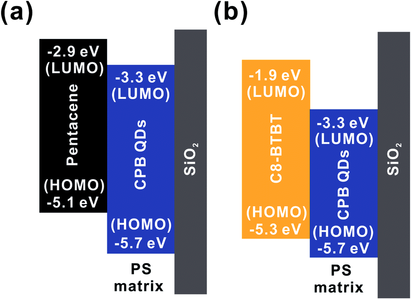
According to the above analysis, the possible electrical programming/photoinduced-reset mechanisms of the C8-BTBT based devices and pentacene based devices are depicted in Fig. 6a–d. First, these two devices have the same electrical program process, that is, as a negative VG was applied on the FGOFETMs under dark (Fig. 6a and c), holes might be transferred from C8-BTBT or pentacene layers to deep-level states of CPB QDs via tunneling because of the low PS thickness. After the holes were trapped into CPB QDs, the concentration of holes in the conductive channel of the FGOFETMs decreased, leading to programmed states. Consequently, the transfer curves moved to the negative direction. At the same time, the trapped holes formed an internal electric field (Ein) between the semiconductor layers and CPB QDs/PS composite floating-gate layer. However, due to their different absorption characteristics of pentacene and C8-BTBT in the visible light region, these two devices have different photoinduced-reset process. The detailed photoinduced-reset process of devices based on C8-BTBT and pentacene are shown in Fig. 6b and d respectively. Upon application of white light illumination, high density of excitons were generated in CPB QDs for C8-BTBT based devices. These excitons were immediately separated into holes and electrons under the existence of Ein. The photo-generated electrons recombined with the holes that trapped in deep-level states of CPB QDs, whereas the shallow level photo-generated holes with high energy would easily escape from CPB QDs to C8-BTBT due to an energetic driving force.38,39 The process increased the concentration of holes in the conductive channel of C8-BTBT and led to the photoinduced-reset behavior. As for pentacene based devices, when they were exposed to white light, excitons could be generated in both pentacene and CPB QDs. Driven by Ein, the excitons generated in pentacene were divided into holes and electrons, the photo-generated holes would flow into the conductive channel of pentacene to enhance the concentration of holes and the photo-generated electrons would undergo downward to recombine with the trapped holes in deep-level states of CPB QDs. The excitons generated in CPB QDs would encounter the same process as those in CPB QDs of C8-BTBT based devices. Finally, the stored charges were eventually depleted in the floating-gate layer and the concentration of holes in the conductive channel of pentacene also increased, leading to transfer curves shifted back to their initial states.
 | ||
| Fig. 6 Operational mechanisms of C8-BTBT based devices operated in (a) electrical programming mode, (b) photoinduced-reset mode. Operational mechanisms of pentacene based devices operated in (c) electrical programming mode, (d) photoinduced-reset mode. | ||
Conclusions
In conclusion, a photoinduced-reset FGOFETM based on pentacene or C8-BTBT has been fabricated using CPB QDs/PS composite floating-gate layer. The C8-BTBT based FGOFETM shows a large memory window (≈90 V) and ultrahigh memory on/off ratio (over 107), which leads to excellent multilevel storage ability in a single OFET and long retention time. These characteristics are believed to originate from the use of CPB QDs/PS composite floating-gate and organic semiconductors with suitable energy levels. In addition, the “photoinduced-reset effect” could be observed in programmed FGOFETMs based on CPB QDs/PS composite film under white light and the corresponding photoinduced-reset mechanism was obtained. Furthermore, the 4 current levels were all steadily maintained over 10 years, indicating our FGOFETM has the highly stable data retention capability. Our devices with good overall performances provide the potential for application in photorecorders and photosensitive smart tags.Conflicts of interest
The authors declare no competing financial interest.Acknowledgements
The authors would like to acknowledge the financial support from National Natural Science Foundation of China (No. 22005270), Zhejiang Provincial Natural Science Foundation of China (No. LQ21E030003), the Education Department Program of Zhejiang Province, China (No. Y201943039), the National Key R&D Program of China (2018YFB1500102), Zhejiang Provincial Key Laboratory (No. 2013E10022).References
- Y. Yu, Q. H. Ma, H. F. Ling, W. Li, R. L. Ju, L. Y. Bian, N. E. Shi, Y. Qian, M. D. Yi, L. H. Xie and W. Huang, Adv. Funct. Mater., 2019, 29, 1904602 CrossRef CAS.
- Y. Park, K.-J. Baeg and C. Kim, ACS Appl. Mater. Interfaces, 2019, 11, 8327–8336 CrossRef CAS.
- X. M. Wu, S. Q. Lan, D. B. Hu, Q. Z. Chen, E. L. Li, Y. J. Yan, H. P. Chen and T. L. Guo, J. Mater. Chem. C, 2019, 7, 9229–9240 RSC.
- R. H. Kim, J. Lee, K. L. Kim, S. M. Cho, D. H. Kim and C. Park, Small, 2017, 13, 1603971 CrossRef.
- M. L. Xu, X. D. Zhang, S. Z. Li, T. Xu, W. F. Xie and W. Wang, J. Mater. Chem. C, 2019, 7, 13477–13485 RSC.
- C.-C. Shih, W.-Y. Lee, Y.-C. Chiu, H.-W. Hsu, H.-C. Chang, C.-L. Liu and W.-C. Chen, Sci. Rep., 2016, 6, 20129 CrossRef CAS.
- K.-J. Baeg, D. Khim, D.-Y. Kim, S.-W. Jung, J. B. Koo and Y.-Y. Noh, J. Phys. Soc. Jpn., 2010, 49, 05EB01 Search PubMed.
- J.-Y. Chen, Y.-C. Chiu, Y.-T. Li, C.-C. Chueh and W.-C. Chen, Adv. Mater., 2017, 29, 1702217 CrossRef.
- X. Hou, H. Zhang, C. S. Liu, S. J. Ding, W. Z. Bao, D. W. Zhang and P. Zhou, Small, 2018, 14, 1800319 CrossRef.
- D. Lee, E. Hwang, Y. Lee, Y. Choi, J. S. Kim, S. Lee and J. H. Cho, Adv. Mater., 2016, 28, 9196–9202 CrossRef CAS.
- H. H. Yang, Y. J. Yan, X. M. Wu, Y. Q. Liu, Q. Z. Chen, G. C. Zhang, S. M. Chen, H. P. Chen and T. L. Guo, J. Mater. Chem. C, 2020, 8, 2861–2869 RSC.
- D. Xiang, T. Liu, J. L. Xu, J. Y. Tan, Z. H. Hu, B. Lei, Y. Zheng, J. Wu, A. H. C. Neto, L. Liu and W. Chen, Nat. Commun., 2018, 9, 2966 CrossRef.
- T. Leydecker, M. Herder, E. Pavlica, G. Bratina, S. Hecht, E. Orgiu and P. Samorì, Nat. Nanotechnol., 2016, 11, 769–775 CrossRef CAS.
- C. Qian, J. Sun, L.-A. Kong, Y. Fu, Y. Chen, J. X. Wang, S. T. Wang, H. P. Xie, H. Huang, J. L. Yang and Y. L. Gao, ACS Photonics, 2017, 4, 2573–2579 CrossRef CAS.
- C.-C. Shih, Y.-C. Chiang, H.-C. Hsieh, Y.-C. Lin and W.-C. Chen, ACS Appl. Mater. Interfaces, 2019, 11, 42429–42437 CrossRef CAS.
- Y. L. Guo, C.-A. Di, S. H. Ye, X. N. Sun, J. Zheng, Y. G. Wen, W. P. Wu, G. Yu and Y. Q. Liu, Adv. Mater., 2009, 21, 1954–1959 CrossRef CAS.
- Y. Zhang, C. L. Lang, J. Z. Fan, L. Shi, Y. P. Yi, Q. J. Yu, F. Y. Guo, J. Wang and L. Zhao, Org. Electron., 2016, 35, 53–58 CrossRef CAS.
- Y. T. Chen, Y. L. Chu, X. H. Wu, W. Ou-Yang and J. Huang, Adv. Mater., 2017, 29, 1704062 CrossRef.
- M. V. Kovalenko, L. Protesescu and M. I. Bodnarchuk, Science, 2017, 358, 745–750 CrossRef CAS.
- Z. L. Chen, Y. T. Zhang, H. Zhang, Y. Yu, X. X. Song, H. T. Zhang, M. X. Cao, Y. L. Che, L. F. Jin, Y. Q. Li, H. T. Dai, J. B. Yang and J. Q. Yao, Appl. Phys. Lett., 2018, 112, 212101 CrossRef.
- Y. Wang, Z. Y. Lv, J. R. Chen, Z. P. Wang, Y. Zhou, L. Zhou, X. L. Chen and S.-T. Han, Adv. Mater., 2018, 30, 1802883 CrossRef.
- M. D. Yi, M. Xie, Y. Q. Shao, W. Li, H. F. Ling, L. H. Xie, T. Yang, Q. L. Fan, J. L. Zhu and W. Huang, J. Mater. Chem. C, 2015, 3, 5220–5225 RSC.
- W. C. Yang, Y. C. Chiang, J. Y. Lam, T. H. Chuang, E. Ercan, C. C. Chueh and W. C. Chen, Adv. Electron. Mater., 2020, 6, 2000458 CrossRef CAS.
- Y. J. Jeong, D.-J. Yun, S. H. Noh, C. E. Park and J. Jang, ACS Nano, 2018, 12, 7701–7709 CrossRef CAS.
- C.-H. Chen, Y. Wang, H. Tatsumi, T. Michinobu, S.-W. Chang, Y.-C. Chiu and G.-S. Liou, Adv. Funct. Mater., 2019, 29, 1902991 CrossRef.
- Y. J. Jeong, D.-J. Yun, S. H. Kim, J. Jang and C. E. Park, ACS Appl. Mater. Interfaces, 2017, 9, 11759–11769 CrossRef CAS.
- M. Y. Liao, Y. C. Chiang, C. H. Chen, W. C. Chen and C. C. Chueh, ACS Appl. Mater. Interfaces, 2020, 12, 36398–36408 CrossRef CAS.
- S.-W. Cheng, T. Han, T.-Y. Huang, Y.-H. Chien Chang, C.-L. Liu, B. Z. Tang and G.-S. Liou, ACS Appl. Mater. Interfaces, 2018, 10, 18281–18288 CrossRef CAS.
- S.-T. Han, Y. Zhou, L. Zhou, Y. Yan, L.-B. Huang, W. Wu and V. Roy, J. Mater. Chem. C, 2015, 3, 3173–3180 RSC.
- H. Klauk, M. Halik, U. Zschieschang, G. Schmid, W. Radlik and W. Weber, J. Appl. Phys., 2002, 92, 5259–5263 CrossRef CAS.
- Y. B. Yuan, G. Giri, A. L. Ayzner, A. P. Zoombelt, S. C. B. Mannsfeld, J. Chen, D. Nordlund, M. F. Toney, J. S. Huang and Z. N. Bao, Nat. Commun., 2014, 5, 3005 CrossRef.
- M. J. Pei, J. Qian, S. Jiang, J. H. Guo, C. D. Yang, D. F. Pan, Q. J. Wang, X. R. Wang, Y. Shi and Y. Li, J. Phys. Chem. Lett., 2019, 10, 2335–2340 CrossRef CAS.
- L. Protesescu, S. Yakunin, M. I. Bodnarchuk, F. Krieg, R. Caputo, C. H. Hendon, R. X. Yang, A. Walsh and M. V. Kovalenko, Nano Lett., 2015, 15, 3692–3696 CrossRef CAS.
- C. C. Shih, Y. C. Chiu, W. Y. Lee, J. Y. Chen and W. C. Chen, Adv. Funct. Mater., 2015, 25, 1511–1519 CrossRef CAS.
- W. Li, F. N. Guo, H. F. Ling, P. Zhang, M. D. Yi, L. Y. Wang, D. Q. Wu, L. H. Xie and W. Huang, Adv. Sci., 2017, 4, 1700007 CrossRef.
- Y. R. Ren, Y. W. Zhu, D. F. Li, P. Wei, W. L. Lu, L. J. Bub and G. H. Lu, J. Mater. Chem. C, 2019, 7, 12862–12868 RSC.
- M. L. Li, J. W. Wang, X. Y. Cai, F. J. Liu, X. J. Li, L. Wang, L. Liao and C. Jiang, Adv. Electron. Mater., 2018, 4, 1800211 CrossRef.
- B. C. Thompson and J. M. J. Frechet, Angew. Chem., Int. Ed., 2008, 47, 58–77 CrossRef CAS.
- I. Gur, N. A. Fromer, M. L. Geier and A. P. Alivisatos, Science, 2005, 310, 462–465 CrossRef CAS.
Footnote |
| † Electronic supplementary information (ESI) available. See DOI: 10.1039/d0ra08021g |
| This journal is © The Royal Society of Chemistry 2020 |