
 Open Access Article
 This Open Access Article is licensed under a Creative Commons Attribution-Non Commercial 3.0 Unported Licence
Preparation of a CuGaSe2 single crystal and its photocathodic properties
Shigeru Ikeda *a,
Wakaba Fujitaa,
Riku Okamotoa,
Yoshitaro Noseb,
Ryoji Katsubeb,
Kenji Yoshinoc and
Takashi Haradad
*a,
Wakaba Fujitaa,
Riku Okamotoa,
Yoshitaro Noseb,
Ryoji Katsubeb,
Kenji Yoshinoc and
Takashi Haradad
aDepartment of Chemistry, Konan University, Kobe, Hyogo 658-8501, Japan. E-mail: s-ikeda@konan-u.ac.jp
bDepartment of Materials Science and Engineering, Kyoto University, Kyoto 606-8501, Japan
cDepartment of Applied Physics and Electronic Engineering, University of Miyazaki, Miyazaki 889-2192, Japan
dResearch Center for Solar Energy Chemistry, Osaka University, Toyonaka, Osaka 560-8531, Japan
First published on 5th November 2020
Abstract
Chalcopyrite CuGaSe2 single crystals were successfully synthesized by the flux method using a home-made Bridgman-type furnace. The grown crystals were nearly stoichiometric with a Se-poor composition. Although a wafer form of the thus-obtained single crystal showed poor p-type electrical properties due to such unfavorable off-stoichiometry, these properties were found to be improved by applying a post-annealing treatment under Se vapor conditions. As a result, an electrode derived from the Se-treated single crystalline wafer showed appreciable p-type photocurrents. After deposition of a CdS ultrathin layer and a nanoparticulate Pt catalyst on the surface of the electrode, appreciable photoelectrochemical H2 evolution was observed over the modified electrode under photoirradiation by simulated sunlight with application of a bias potential of 0 VRHE.
1. Introduction
Wide-gap chalcopyrite materials have been attractive materials for efficient utilization of sunlight energy because of their potential applications for a wide variety of devices. One of the significant applications is as a top cell in tandem solar cells.1 for example, S- and Ga-based chalcopyrite materials, namely Cu(In,Ga)S2 and CuGaSe2, have shown high potential with over 10% sunlight conversion efficiencies.2 The other possible application of these materials is photoelectrochemical (PEC) conversion of sunlight energy into chemical energy. Specifically, PEC water splitting for hydrogen (H2) generation is a representative example of the PEC system; several studies have demonstrated successful evolution of H2 by using CuGa(S,Se)2, Cu(In,Ga)Se2, and Cu(In,Ga)S2.3 As an another typical system among the PEC energy conversion system, we have proved the applicability of S-based wide-gap chalcopyrite CuGaS2 for PEC reduction of carbon dioxide (CO2).4 However, all of these wide-gap-chalcopyrite-based PEC systems reported did not reach the necessary level for applying a realistic system and thereby recent studies on these PEC systems have also focused on developments of several candidates other than these chalcopyrite materials.5For the application of chalcopyrite and related materials to PEC systems, thin film forms are usually utilized. As mentioned above, one of the reasons is of curse their successful applications in photovoltaic systems. Among the various thin film growth techniques, the co-evaporation process is the best method for obtaining high photovoltaic and PEC efficiencies.6 An alternative non-vacuum spray deposition method is also a promising method for obtaining wide-gap chalcopyrite thin films for photovoltaic and PEC applications.7 As is well known empirically, however, these techniques are only applicable to chalcopyrite compounds with limited compositions: thus-obtained compound thin films other than these materials often have small grain sizes, insufficient compactness, and/or remaining secondary phases inappropriate not only for photovoltaic applications but also PEC usages.8
In order to find new materials efficient for PEC applications, therefore, fundamental studies by using well-grown bulk crystals as model materials are needed. Specifically, high-quality single crystals are desirable to investigate the fundamentals of bulk properties such as the effects of intrinsic point defects, grain boundaries and nanocomposites on reduction of carrier diffusion lengths as well as factors controlling electrical properties induced by extrinsic doping, compositional deviations, and alloying with other elements. In this study, we focused on CuGaSe2 as an example of p-type materials applicable for several PEC applications and investigated the growth of CuGaSe2 single crystals using a traveling heater technique. Structural, electrical, and PEC properties of the thus-obtained single crystal as well as successful demonstration of PEC hydrogen production over a photocathode based on the CuGaSe2 single crystal are reported.
2. Experimental
2.1 Growth of CuGaSe2 single crystals
The growth of a CuGaSe2 single crystal was performed by a unidirectional solidification of Cu–Ga–Se solutions using a home-made vertically aligned Bridgman (type) furnace as was used for the growth of ZnSnP2 and In-doped Zn3P2.9 Source materials were elemental shots of constituent elements (Cu (99.99%), Ga (99.9999%), and Se (99.999%)) purchased from Kojundo Chemical Laboratory. The elemental shots with compositional ratios of Cu/Ga/Se = 35.0/22.5/42.5 were charged into a carbon-coated quartz ampoule with an inner radius of 7 mm and length of ca. 20 mm at Pa below 10−3 and then sealed off. Prior to sealing, starting Cu and Ga shots were etched with 1 M HCl for 1 min to remove surface contaminants and then rinsed in distilled water. The sealed ampoule was passed through the vertical zone melting furnace. The temperature at the initial point and temperature gradient in the furnace were controlled by three separate coil heaters. During the single crystal growth, travelling velocity of the ampoule in the downward direction was fixed at 1 cm per day. The thus-obtained grown CuGaSe2 crystal was cut into wafers with diameters of 7 mm and thicknesses of ca. 0.5 mm. The surface of each wafer was mechanically polished with emery papers and finally with 1 μm of diamond slurry on a buff sheet. The single crystal was also pulverized in a mortar for crystallographic measurements (see below).2.2 Characterization
Crystallographic structures were determined by X-ray diffraction (XRD) analyses using a Panalytical X'Pert Pro Alpha-1 diffractometer (Cu Kα, Ni filter) and Raman spectroscopy using a JASCO NRS 3100 laser Raman spectrophotometer (532 nm). Elemental distributions of wafer-form samples were analysed by using a JEOL JCM-6000 Plus scanning electron microscope (SEM) equipped with a JEOL MP-05030-EDK energy dispersive X-ray spectrometer (EDS). The electrical properties were analysed by using a TOYO ResiTest8300 Hall effect measurement system in a 0.45 T magnetic field in the Van der Pauw geometry. For electrical measurements, Au contacts, each with a diameter of 1 mm and thickness of about 200 nm, were deposited by thermal evaporation onto the corners of a sample.2.3 PEC analyses
PEC measurements were performed using a conventional three-electrode setup. Three electrodes, namely, Pt wire, Ag/AgCl, and CuGaSe2 wafer-based electrode, as counter, reference, and working electrodes, respectively, were inserted into a three-necked flask with a flat window containing 0.2 M Eu(NO3)3 solution (pH 4). The CuGaSe2 wafer-based electrodes were prepared by deposition of an Mo back contact on the polished surface of a CuGaSe2 wafer by direct current (DC) sputtering followed by adhesion to an FTO-coated glass substrate using a silver paste. Since the Eu3+ ion works as an efficient electron acceptor for the p-type photocathode,10 the thus-obtained CuGaSe2 wafer-based electrode without any surface modifications was used. The potential sweep was controlled by a Hokuto Denko HSV-110 automatic polarization system. Measurements were conducted by a linear sweep voltammetric (LSV) mode with a negative scan direction at the scan rate of 10 mV s−1 under chopped illumination of simulated sunlight (AM 1.5G) using an Asahi Spectra HAL320 solar simulator.In order to examine water reduction (H2 production) properties of the CuGaSe2 wafer-based electrode, surface modification by a CdS thin layer followed by deposition of Pt particles was performed. For the CdS modification, the CuGaS2 wafer-based electrode was immersed in an aqueous solution containing 12.5 mM CdSO4, 0.22 M thiourea and 11 M NH4OH at 60 °C for 7 min. After washing with demineralized water, the CdS-modified wafer electrode was put into the above-described PEC setup. The electrolyte used for the Pt deposition was composed of 0.1 M Na2SO4 and 1 mM H2PtCl6 at pH adjusted to 4 using a diluted HCl solution; photoirradiation was performed by using a Cermax LX-300F 300 W xenon lamp at a fixed potential of −0.7 V (vs. Ag/AgCl) for 30 s. An LSV plot for the water reduction over the thus-obtained Pt- and CdS-modified wafer electrode under chopped illumination of simulated sunlight (AM 1.5G) was recorded at pH 6.5 using a phosphate buffer solution (0.2 M Na2HPO4/NaH2PO4) as an electrolyte. Potentials for the PEC water reduction that referred to the Ag/AgCl electrode (VAg/AgCl) were converted to those that referred to the reversible hydrogen electrode (VRHE) by using the following equation:
| VRHE = VAg/AgCl + 0.059 × pH + 0.199. |
A PEC cell connected to an online gas chromatography system (Agilent 490 Micro GC Gas Analyzer equipped with an MS-5A column and a thermal conductivity detector) was used to obtain a time course curve of H2 liberation. The PEC cell was immersed in a water bath to maintain the temperature at 293 K, and photoirradiation was performed at 0 VRHE under illumination of simulated sunlight (AM 1.5G).
3. Results and discussion
3.1 Crystallographic properties
The compositional ratio for the single crystal growth was determined by a phase diagram of the pseudo-binary Cu2Se–Ga2Se3 system reported in the literature.11 In order to avoid formation of a Cu-deficient undesired phase, we chose a Cu-excess composition (see Experimental) to grow a CuGaSe2 single crystal; it is likely to grow in a Cu–Ga–Se flux under the present conditions. The Bridgman-type furnace used was composed of three heaters; temperatures of upper, main, and bottom heaters were set to 1020 °C, 1010 °C and 1000 °C, respectively. The temperature profile of the furnace produced by these set temperatures is shown in Fig. 1a. According to the reported phase diagram,11 the melting point at the present charged composition is ca. 1020 °C. Thus, actual temperatures from the initial point (14 cm from the bottom of the furnace) to ca. 30 cm in the upper part were kept above that temperature. After several trials, the optimum traveling velocity of the ampoule in the downward direction at the present temperature gradient was determined to be 1 mm per day, i.e., it took 14 days for completion of the growth experiment. A typical photograph of the thus-obtained ingot is shown in Fig. 1b. The rod-shaped ingot was 7 mm in diameter and 70 mm in length. In subsequent experiments, we used a ca. 5–30 mm part from the tip of the ingot. | ||
| Fig. 1 (a) Temperature profile of the growth furnace used and (b) photograph of the thus-obtained ingot. | ||
The powder XRD pattern of the thus-obtained crystal is shown in Fig. 2a. The XRD pattern exhibited major peaks corresponding to diffraction patterns of the chalcopyrite structure of CuGaSe2 (ICDD #01-076-1735). There was no reflection assignable to probable impurities such as CuxSe. Observations of clear peak separations between the (220) and (204) planes as well as between the (312) and (116) planes indicated the absence of analogous Cu-deficient CuGa3Se5 and CuGa5Se8 secondary phases.12 In addition, an XRD pattern of a wafer form obtained by cutting the ingot perpendicular to the growth direction did not show appreciable diffraction, though it showed an unknown spike at ca. 29° that was probably due to an artifact (Fig. 2b), implying that the sample is a single crystal. Raman spectroscopy was performed in order to further confirm the formation of phase pure CuGaSe2. As shown in Fig. 2c, the Raman spectrum exhibited an intense peak at 184 cm−1 in addition to a broad band at ca. 225–255 cm−1, which corresponded to the reported Raman spectrum of CuGaSe2.13 The absence of a distinct peak assignable to CuGa3Se5 (166 cm−1)14 or CuxSe (around 260 cm−1)15 in the spectrum indicated the formation of phase-pure CuGaSe2, being consistent with the above-described XRD results.
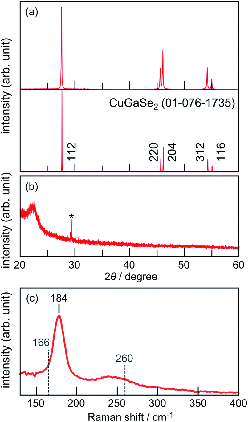 | ||
| Fig. 2 (a) XRD pattern of the thus-obtained ingot measured by a powdered form of the sample and (b) corresponding XRD pattern of the ingot obtained by cutting the ingot perpendicular to the growth direction. (c) Raman spectra of the powdered form of the ingot. Reference XRD profile of CuGaSe2 (ICDD #01-076-1735) shown in panel (a) was obtained by VESTA software. Asterisk (*) in panel (b) denotes an unidentified spike. | ||
3.2 Compositional and electric properties
The composition of a CuGaSe2 single crystal was analysed by EDS using wafer forms of samples obtained by cutting the ingot ca. 5–30 mm from the end perpendicular to the growth direction (see Fig. 1b). Fig. 3a–c show EDS mappings of main elements of the wafer formed sample thus obtained. It was confirmed that the main elements of Cu, Ga and Se are seemed to be homogeneously distributed. Average Cu, Ga, and Se contents estimated by analyses of 45 positions (45 squares with the length of each side being ca. 10 μm) in an SEM image of the wafer were determined to be 26.75 ± 0.14%, 26.03 ± 0.17%, and 47.22 ± 0.25%, respectively (Fig. 3d, left). Significantly low values of errors, defined as the confidence interval (99%), indicate homogeneous distribution of these elements, as expected from the above EDS mappings. The compositional ratio of Cu to Ga (Cu/Ga) was almost stoichiometric but that of Se to the sum of Cu and Ga (Se/(Cu + Ga)) was appreciably lower than unity, indicating that the present CuGaSe2 single crystal was deviated to the Se-poor composition compared to its stoichiometry. It is known that p-type conductivity is derived from the Cu vacancy (VCu); the Se vacancy (VSe) is a typical n-type defect.16 Therefore, for the use of a p-type photocathode material, the CuGaSe2 single crystal obtained in this study has an unfavourable off-stoichiometry composition. The off-stoichiometry of the CuGaSe2 single crystals is likely to be tuneable by compositional control of the source Cu–Ga–Se mixture. Such studies are now in progress.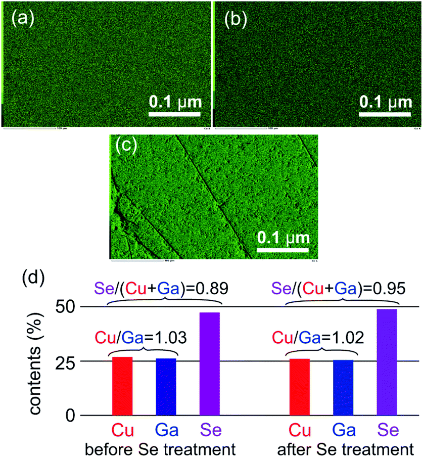 | ||
| Fig. 3 (a) Cu, (b) Ga and (c) Se EDS mappings and (d) average compositions of Cu, Ga, and Se elements of the wafer form of a CuGaSe2 single crystal. Average compositions of Cu, Ga, and Se elements of the sample after applying Se annealing is also shown in panel (d). | ||
The electrical properties of the CuGaSe2 single crystal analysed by the Van der Pauw method are summarized in Table 1. The hole concentration (p), conductivity (σ), and mobility (μh) obtained by results of Hall effect measurements at room temperature were estimated to be 6.3 × 1014 cm−3, 1.6 × 10⁻⁴ S cm−1, and 0.28 cm2 V−1 s−1, respectively. As mentioned above, significantly low p, σ, and μh values of the present CuGaSe2 single crystal are attributed to its unfavourable off-stoichiometry composition (i.e., Se-poor composition). In order to improve these electric properties, annealing treatment was applied to the CuGaSe2 single crystalline wafer at 750 °C for 10 h in an Se vapor condition. Elemental compositions of Cu, Ga, and Se of thus-obtained sample calculated by EDS analyses indicated appreciable increment of the Se content (Fig. 3d), suggesting a partial compensation of the VSe vacancy. As we expected, the p value was improved by two figures accompanied by significant increase in σ and μh values (Table 1).
| Sample | p (cm−3) | σ (S cm−1) | μh (cm2 V−1 s−1) |
|---|---|---|---|
| W/o annealing | 7.0 × 10¹⁴ | 9.2 × 10⁻⁵ | 0.82 |
| After annealing | 2.9 × 10¹⁶ | 5.4 × 10⁻² | 11.6 |
3.3 PEC characteristics
PEC current–voltage characteristics of CuGaSe2 single crystals were investigated by LSV measurement in an aqueous Eu3+ solution. An electrode based on the wafer form of a CuGaSe2 single crystal was obtained by formation of an ohmic contact with an FTO/glass substrate by interposing an Mo layer. Although a p-type semiconducting feature appeared in the Hall effect measurements, the CuGaSe2 single crystal-based electrode did not show an appreciable p-type PEC characteristic: there was almost no current flow in the whole range measured because of its high resistivity (Fig. 4). On the other hand, when the electrode was prepared by using a CuGaSe2 single crystal wafer annealed in Se vapor at 750 °C for 10 h, significant photocurrents appeared, as expected from the results of electrical property measurements. Although the exact photocurrent onset is not clear owing to the appearance of a positive dark current derived from the shunt, it is assumed to be ca. −0.05 V (vs. Ag/AgCl), which is close to the value of several sulfur (S)-based p-type chalcopyrite and related compound thin films applied to solar cells and PEC water splitting.7,17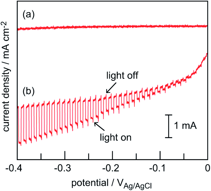 | ||
| Fig. 4 LSV plots of CuGaSe2 single crystal-based electrodes based on (a) a bare CuGaSe2 single crystal (w/o Se annealing) and (b) a CuGaSe2 single crystal after applying Se annealing in 0.1 M europium nitrate under chopped illumination of simulated sunlight (AM 1.5G). | ||
3.4 PEC water reduction properties
We attempted to construct a photocathode specified to water reduction by applying appropriate surface modifications2,4,7,16 to the CuGaSe2 wafer-based electrode. Fig. 5a shows an LSV plot in a pH 6.5 phosphate buffer solution obtained by a CuGaSe2 wafer-based electrode modified with a CdS layer and Pt deposits (Pt–CdS/CuGaSe2) under chopped illumination of simulated sunlight (AM 1.5G). A gradual increment of photocurrents with increase in cathodic polarization was obtained, though appreciable dark currents also existed. The primary event inducing the observed photocurrents is likely to be water reduction into H2. In order to measure gas-phase H2 quantitatively, H2 liberation over the Pt–CdS/CuGaSe2 electrode at a fixed potential (VRHE = 0) was examined. Fig. 5b shows a time course curve of H2 liberation from a unit area of the electrode under illumination of simulated sunlight (AM 1.5G). A current density profile during photoirradiation is also shown in this figure. As expected, a monotonous increase in H2 was observed, though a gradual decrease in the amount of H2 accompanied by a drop in current density appeared in the initial 6 h photoirradiation. The rate of H2 liberation estimated from the slope of the plot at the latter half part (6–11 h) was ca. 2.4 μmol h−1. Although the value is as low as values obtained for several thin-film-based photocathodes, this is the first demonstration of detection of actual H2 liberation over a chalcopyrite-based single crystalline electrode. Faradic efficiency, defined as the ratio in percent of the amount of H2 evolution to that of half electrons passing through the outer circuit (e−/2), was estimated to be 72%, suggesting inclusion of an unfavourable side reaction as was observed by significant dark currents in the LSV plot (see Fig. 5a) Thus, further improvement in the quality of the CuGaSe2 single crystal as well as optimizations of procedures and/or structures of surface modifications are now in progress.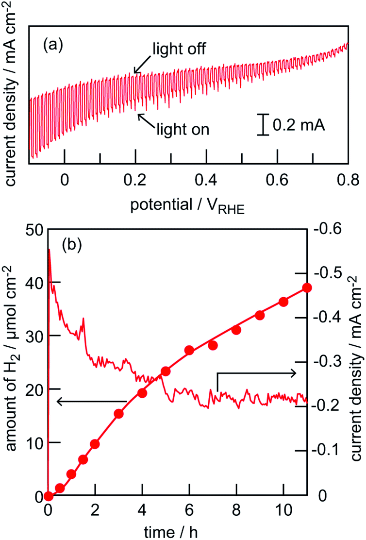 | ||
| Fig. 5 (a) A LSV plot of the Pt–CdS/CuGaSe2 electrode based on a CuGaSe2 single crystal after applying Se annealing under chopped illumination of simulated sunlight (AM 1.5G). (b) Time course curves of H2 liberation and current flow over the electrode during photoirradiation of simulated sunlight (AM 1.5G) with application of a constant bias (0 VRHE). A pH 6.5 phosphate buffer solution (0.2 M Na2HPO4/NaH2PO4) was used as an electrolyte for water reduction experiments. | ||
4. Conclusions
We reported the growth of a p-type CuGaSe2 single crystal in a Cu–Ga–Se flux and its physicochemical properties. Applications of optimal growth temperature, optimal temperature gradient in the furnace, and optimal traveling velocity of the ampoule containing the source materials led to successful formation of phase-pure chalcopyrite CuGaSe2, as confirmed by XRD and Raman spectroscopy analyses. The composition ration of the thus-obtained CuGaSe2 single crystal was found to be Se-poor compared to its stoichiometric ratio. Although the composition is not optimal for photovoltaic and PEC applications, post-annealing in Se vapor was found to be effective to compensate the Se-vacancy and thus leading to an appreciable p-type PEC function. As a result, the CuGaSe2 single crystal was proved to be applicable for PEC H2 production from water after the appropriate surface modification. The results, therefore, suggest that a single crystalline wafer form of a compound semiconductor would be a useful reference to study intrinsic properties and potentials of compound semiconductors that are applicable for several PEC systems for sunlight-to-chemical-energy conversion.Conflicts of interest
There are no conflicts to declare.Acknowledgements
This work was performed under the Hirao Taro Foundation of KONAN GAKUEN for Academic Research and Kinoshita Memorial Foundation. This work was also supported by JSPS Grants-in-Aid for Scientific Research (KAKENHI), awards no. 19H02822 and 20H05120. Prof. Takahiro Wada (Ryukoku University) is acknowledged for his suggestions about structural characterizations.Notes and references
- T. K. Todorov, D. M. Bishop and Y. S. Lee, Sol. Energy Mater. Sol. Cells, 2018, 180, 350–357 CrossRef CAS; K. Kim, S. K. Ahn, J. H. Choi, J. Woo, Y.-J. Eo, J.-S. Cho, A. Cho, J. Gwak, S. Song, D.-H. Cho, Y.-D. Chung and J. H. Yun, Nano Energy, 2018, 48, 34–35 Search PubMed.
- S. Merdes, D. Abou-Ras, R. Mainz, R. Klenk, M. Ch. Lux-Steiner, A. Meeder, H. W. Schock and J. Klaer, Prog. Photovolt: Res. Appl., 2013, 21, 88–93 CrossRef CAS; F. Larsson, N. S. Nilsson, J. Keller, C. Frisk, V. Kosyak, M. Edoff and T. Törndahl, Prog. Photovolt: Res. Appl., 2017, 25, 755–763 CrossRef; J. Kim, H. Hiroi, T. K. Todorov, O. Gunawan, M. Kuwahara, T. Gokmen, D. Nair, M. Hopstaken, B. Shin, Y. S. Lee, W. Wang, H. Sugimoto and D. B. Mitzi, Adv. Mater., 2014, 26, 7427–7431 CrossRef; S. Ishizuka, Phys. Status Solidi A, 2019, 216, 1800873 CrossRef.
- M. Moriya, T. Minegishi, H. Kumagai, M. Katayama, J. Kubota and K. Domen, J. Am. Chem. Soc., 2015, 135, 3733–3735 CrossRef CAS; A. D. DeAngelis, K. Horsley and N. Gaillard, J. Phys. Chem. C, 2018, 122, 14304–14312 CrossRef; H. Kobayashi, N. Sato, M. Orita, Y. Kuang, H. Kaneko, T. Minegishi, T. Yamada and K. Domen, Energy Environ. Sci., 2018, 11, 3003–3009 RSC; N. Gaillard, D. Prasher, M. Chong, A. Deangelis, K. Horsley, H. A. Ishii, J. P. Bradley, J. Varley and T. Ogitsu, ACS Appl. Energy Mater., 2019, 2, 5515–5524 CrossRef.
- S. Ikeda, Y. Tanaka, T. Kawaguchi, S. Fujikawa, T. Harada, S. Nakanishi, T. Takayama, A. Iwase and A. Kudo, Chem. Lett., 2018, 47, 1424–1426 CrossRef CAS.
- H. Kaneko, T. Minegishi, M. Nakabayashi, N. Shibata, Y. Kuang, T. Yamada and K. Domen, Adv. Funct. Mater., 2016, 26, 4570–4577 CrossRef CAS; C. P. Muzzillo, W. E. Klein, Z. Li, A. D. DeAngelis, K. Horsley, K. Zhu and N. Gaillard, ACS Appl. Mater. Interfaces, 2018, 10, 19573–19579 CrossRef; F. Jiang, Gunawan, T. Harada, Y. Kuang, T. Minegishi, K. Domen and S. Ikeda, J. Am. Chem. Soc., 2015, 137, 13691–13697 CrossRef; K. Wang, D. Huang, L. Yu, K. Feng, L. Li, T. Harada, S. Ikeda and F. Jiang, ACS Catal., 2019, 9, 3090–3097 CrossRef; S. Ikeda, S. Fujikawa, T. Harada, T. H. Nguyen, S. Nakanishi, T. Takayama, A. Iwase and A. Kudo, ACS Appl. Energy Mater., 2019, 2, 6911–6918 CrossRef; Y. F. Tay, S. S. Hadke, M. Zhang, N. Lim, S. Y. Chiam and L. H. Wong, J. Mater. Chem. A, 2020, 8, 8862–8867 RSC.
- A. M. Gabor, J. R. Tuttle, D. S. Albin, M. A. Contreras, R. Noufi and A. M. Hermann, Appl. Phys. Lett., 1994, 65, 198–200 CrossRef CAS.
- S. Ikeda, M. Nonogaki, W. Septina, G. Gunawan, T. Harada and M. Matsumura, Catal. Sci. Technol., 2013, 3, 1849–1854 RSC; W. Septina, M. Kurihara, S. Ikeda, Y. Nakajima, T. Hirano, Y. Kawasaki, T. Harada and M. Matsumura, ACS Appl. Mater. Interfaces, 2015, 7, 6472–6479 CrossRef CAS; W. Septina, Gunawan, S. Ikeda, T. Harada, M. Higashi, R. Abe and M. Matsumura, J. Phys. Chem. C, 2015, 119, 8576–8583 CrossRef; W. Septina, M. Sugimoto, D. Chao, Q. Shen, S. Nakatsuka, Y. Nose, T. Harada and S. Ikeda, Phys. Chem. Chem. Phys., 2017, 19, 12502–12508 RSC.
- S. Wang, T. Nazuka, H. Hagiya, Y. Takabayashi, S. Ishizuka, H. Shibata, S. Niki, M. M. Islam, K. Akimoto and T. Sakurai, J. Electron. Mater., 2018, 47, 4944–4949 CrossRef CAS.
- S. Nakatsuka, H. Nakamoto, Y. Nose, T. Uda and Y. Shirai, Phys. Status Solidi C, 2015, 12, 520–523 CrossRef CAS; R. Katsube, H. Hayashi, A. Nagaoka, K. Yoshino, Y. Nose and Y. Shirai, Jpn. J. Appl. Phys., 2016, 55, 041201 CrossRef.
- J. J. Scragg, P. J. Dale and L. M. Peter, Electrochem. Commun., 2008, 10, 639–642 CrossRef CAS; S. Ikeda, T. Nakamura, S. M. Lee, T. Yagi, T. Harada, T. Minegishi and M. Matsumura, ChemSusChem, 2011, 4, 262–268 Search PubMed.
- O. M. Strok, I. D. Olekseyuk, O. F. Zmiy, I. A. Ivashchenko and L. D. Gulay, J. Phase Equilib. Diffus., 2013, 34, 94–103 CrossRef CAS.
- K. Ueda, T. Maeda and T. Wada, Thin Solid Films, 2017, 633, 23–30 CrossRef CAS.
- C. Rincón and F. J. Ramírez, J. Appl. Phys., 1992, 72, 4321–4324 CrossRef.
- C. Rincón, S. M. Wasim, G. Marin, J. M. Delgado, J. R. Huntzinger, A. Zwick and J. Galibert, Appl. Phys. Lett., 1998, 73, 441–443 CrossRef.
- C. Xue, D. Papadimitriou, Y. S. Raptis, W. Richter, N. Esser, S. Siebentritt and M. Ch. Lux-Steiner, J. Appl. Phys., 2004, 96, 1963–1966 CrossRef CAS.
- T. Maeda and T. Wada, J. Phys. Chem. Solids, 2005, 66, 1924–1927 CrossRef CAS.
- T. H. Nguyen, T. Kawaguchi, J. Chantana, T. Minemoto, T. Harada, S. Nakanishi and S. Ikeda, ACS Appl. Mater. Interfaces, 2018, 10, 5455–5463 CrossRef CAS.
| This journal is © The Royal Society of Chemistry 2020 |