DOI:
10.1039/D0RA07776C
(Paper)
RSC Adv., 2020,
10, 42172-42177
Synthesis of 2D MoS2(1−x)Se2x semiconductor alloy by chemical vapor deposition†
Received
10th September 2020
, Accepted 6th November 2020
First published on 20th November 2020
Abstract
Alloying/doping in two-dimensional (2D) materials is emerging as an increasingly important strategy due to the wide-range bandgap tunability and versatility of these materials. Monolayer 2D transition metal dichalcogenide (TMD) alloy has been investigated both theoretically and experimentally in recent years. Here, we synthesized a bilayer MoS2(1−x)Se2x semiconductor alloy via the chemical-vapor deposition technique. The as-grown triangular MoS2(1−x)Se2x flakes with size of roughly 10 μm were observed by optical microscope and scanning electron microscope (SEM). The 1.4–1.9 nm thickness of the samples, as measured by AFM, means that bilayer MoS2(1−x)Se2x alloys were grown. The characteristic Raman modes related to Mo–S and Mo–Se vibrations were observed in the Raman spectrum. Two emission peaks were respectively found, corresponding to the A and B excitons in the photoluminescence (PL) spectrum. XPS measurements confirmed the Se doping of the alloy. The first-principles calculation results show a contraction of the band gap value with the increase of Se doping in the MoS2 lattice. Compared with monolayer MoS2(1−x)Se2x alloy, the band bending effect is more obvious, and the bilayer MoS2(1−x)Se2x alloy still shows the direct band gap luminescence characteristic, which has certain guiding significance for the growth of two-dimensional materials and for device preparation.
Introduction
The transition-metal dichalcogenides have attracted intense attention due to their unique physical properties, and they have potential application as efficient electrodes in photoelectrochemical solar cells,1–3 the catalyst industry, and in secondary batteries4–6 or solid-state lubricants.7 The typical transition-metal dichalcogenides MoS2 and MoSe2 have a structure composed of three similar sublayers: one layer of Mo atom sandwiched by two planes of S or Se atoms, and their bandgap variability is from 1.8 to 1.5 eV. Moreover, theoretical calculation and experimental work showed that the mixed layered crystals with thermodynamic stability allow continuous tuning of the band gap,8 which enhances the application of the 2D transition-metal dichalcogenides in electronic and optoelectronic devices.9,10 Among all kinds of approaches for tuning the bandgap, such as alloying/doping TMDs with other elements,11 strain12 or stacking in the form of heterostructures,13 alloying/doping provides an easily scalable route to engineer the band structure.14,15
A variety of methods have been demonstrated in previous studies to synthesize monolayer MoS2(1−x)Se2x, including mechanical exfoliation of bulk material,16 gentle sputtering,17 physical vapor deposition,18 and chemical vapor deposition.19 Among these methods, the CVD technique is considered a promising method for the controllable synthesis of MoS2(1−x)Se2x flakes, particularly for fabricating monolayer MoS2(1−x)Se2x. Also, theoretical (ab initio) calculations have been performed to reveal the modification of the band structure and bandgap of monolayer MoS2 with Se doping.20 In order to explore the bandgap difference between bilayer and monolayer MoS2(1−x)Se2x, the MoS2(1−x)Se2x flakes were synthesized by the low-pressure chemical vapor deposition technique. The difficulty in synthesizing MoS2(1−x)Se2x bilayer is in controlling the growth parameters in the alloying process, such as deposition temperature, evaporation concentration, and pressure for deposition. The bilayer MoS2(1−x)Se2x alloys are found to be achieved easily when x is smaller than 50% in Ar atmosphere.
Experiments
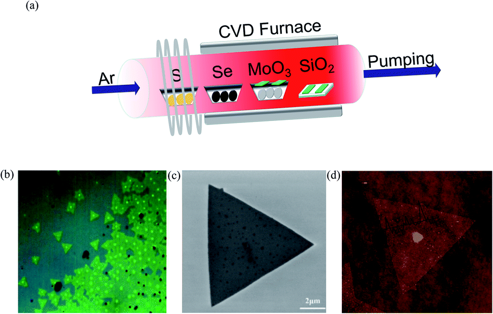
In the present work, MoS2 bilayer and MoSe2 bilayer with controllable morphology and size were firstly obtained using chemical vapor deposition (CVD), and the optical bandgaps of the resulting compounds are 1.53 and 1.82 eV, as given by photoluminescence spectra. Then, we explore the bandgap of MoS2(1−x)Se2x bilayer as a function of Se/S ratio. The growth of MoS2(1−x)Se2x sheets was carried out in a three-zone tube furnace with a 2.5-inch diameter quartz tube, as shown in Fig. 1(a), where different shades of red indicate different temperatures. Sulfur, selenium and molybdenum trioxide precursors were loaded in ceramic boats and were placed from downstream to upstream in the furnace tube, respectively. Argon gas of 200 sccm was provided throughout the experiment. The furnace was heated to 650 °C at a rate of 10 °C min−1; in the meantime, selenium was heated to 350 °C and sulfur was heated to 250 °C by heating belt. When the furnace reached 850 °C, the argon gas carries the vaporized selenium, sulfur and molybdenum trioxide to the substrates during the deposition process. After the growth, the furnace was naturally cooled to room temperature. The heating and cooling process of the tube furnace in the experiment is shown in Fig. S1.† More details of the experiment can be seen in the ESI.†
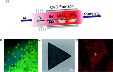 |
| | Fig. 1 (a) Illustration of the three-heating-zone furnace setup for MoS2(1−x)Se2x growth; (b) OM image, (c) SEM image and (d) AFM image of bilayer MoS2(1−0.37)Se2(0.37). | |
Results and discussion
A typical optical image of the as-grown bilayer MoS2(1−0.37)Se2(0.37) is shown in Fig. 1(b). It is not difficult to find some dots distributed within the surface of the MoS2(1−x)Se2x samples. The bright dot located at the center of the nanoflake indicates the original nucleation sites for the crystals. Similar to the perylene-3,4,9,10-tetracarboxylic acid tetrapotassium salt (PTAS) of MoS2,21 we can conclude that these bright dots coming from PTAS serve as a seeding promoter for the growth of the MoS2(1−x)Se2x. The shape and scale of MoS2(1−0.37)Se2(0.37) are given by the SEM images shown in Fig. 1(b). Unlike SbTe2,22 α-MoO3 (ref. 23) and Bi2Se3,24 MoS2 (ref. 25) and MoSe2 (ref. 26) grow in the triangular direction. By controlling the quantity of evaporation source, triangles of MoS2(1−x)Se2x with a size >5 μm were obtained. It is noteworthy that the morphology of the material will not be influenced by the composition. As displayed in Fig. 1(c), the thickness and morphology of MoS2(1−0.37)Se2(0.37) was further confirmed by AFM technique. The height profile from the Si/SiO2 substrate to the triangular regions falls in the range of 1.4 nm, which is in good relation to the thickness of the MoS2(1−0.37)Se2(0.37) bilayer.
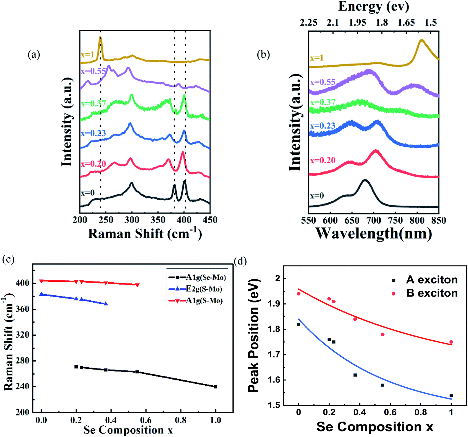
Raman spectroscopy (wavelength of laser, 514 nm) was used to investigate the structure of the MoS2(1−x)Se2x samples. Two sets of Raman peaks are observed in Fig. 2(a). One set of Raman peaks are MoS2-like peaks around 380–400 cm−1, which can be attributed to the E1 2g mode resulting from in-plane vibration and the A1g mode originating from out-of-plane vibration.27 Also, the intensity of A1g mode is higher than that of E1 2g mode because the intralayer bonding is thought to be strong and predominantly covalent, whereas the interlayer weak bonding is of the van der Waals type.28 The other set, consisting of 240 and 280 cm−1 peaks, corresponds to MoSe2-like A1g and E1 2g modes, but slightly shifts to lower wavenumber values than those of pure MoSe2.29 Apart from these peaks, the spectrum contains a peak around 300 cm−1, which is independent of the composition.30 It is reasonable to infer that the peak is ascribed to the silicon substrate. It should be noted that the original material MoS2 bilayer has two Raman modes, as earlier reported, and by introducing the Se during the growth process, the synthesized MoS2(1−x)Se2x alloy presents two sets of Raman modes. Moreover, with the increasing Se component, the intensity of MoS2-like modes weakens gradually and finally disappears, but the intensity of MoSe2-like modes is enhanced, which agrees with the reported result of monolayer material.31 In addition, the kind and intensity of Raman peaks were changed with the introduction of Se to the original MoS2, as shown in Fig. 2(c). All peaks are shifted to lower wavenumbers with increasing Se content, which is consistent with the behavior of monolayer MoS2(1−x)Se2x.32 The pristine monolayer MoS2 consists of three sublayers, one layer of Mo atom sandwiched by two planes of sulfur atoms. As the Se atoms substitute for a part of the S sites, the symmetry of original MoS2 crystals is broken due to the larger radius of Se atoms.33 The original Mo–S and Mo–Mo bond lengths are changed by the distortion, leading to an external tensile stress exerting on the original MoS2 lattice. Therefore, the atomic vibration due to the E1 2g and A1g modes of MoS2 is softened.34
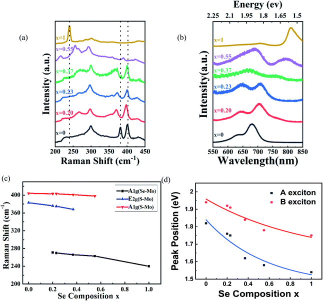 |
| | Fig. 2 (a) Raman spectra and (b) PL spectra of the bilayer MoS2(1−x)Se2x (x = 0.00–1.00); (c) plots of MoS2(1−x)Se2x Raman modes with Se composition increasing; (d) plots of A-exciton and B-exciton energy of MoS2(1−x)Se2x. | |
Photoluminescence measurements were performed to study the optical properties of as-grown MoS2(1−x)Se2x. We control the composition of the alloy by adjusting the amount of reactants Se, S and MoO3. The photoluminescence spectra of the bilayer MoS2(1−x)Se2x (x = 0–1) are shown in Fig. 2(b). In comparison with monolayer MoS2(1−x)Se2x, all bilayer alloys have two PL peaks originating from the direct excitonic transition at the K-point of the first Brillouin zone.35 The peak located at the higher wavelength is generally termed as exciton A, and the other at the lower wavelength as exciton B.36 The difference between these PL peaks can be inferred from the spin–orbit coupling of the valence band.37 The plots of A and B exciton energy of bilayer MoS2(1−x)Se2x with different Se contents (x) are displayed in Fig. 2(d). The results reveal that the emission energy can be continually tuned from 1.82 eV (680 nm) to 1.53 eV (810 nm). We find a decrease of the optical bandgap with Se content increasing in the bilayer MoS2(1−x)Se2x alloy, which is similar to monolayer MoS2(1−x)Se2x. However, the bandgap bowing effect is more obvious than that in monolayer MoS2(1−x)Se2x.38 There is no doubt that the redshift of PL peaks is related to the band structure variation via Se introduction to MoS2. According to the molecular orbital theory, the non-bonding d bands of MoS2 are mainly derived from the Mo-dz2, Mo-dx2−y2,xy and Mo-dxz,yz orbitals.39,40 Mo and S atoms are coordinated through ionic–covalent interaction. With Se introduction into MoS2, the strong covalent effects in MoS2(1−x)Se2x subsequently occur, resulting in the non-bonding d bands broadening and, thus, the band gap reduced.28,39 Beyond the optical properties based on PL, we evaluated the stoichiometric features of bilayer MoS2(1−x)Se2x.
According to the following formula, a quadratic rule is introduced to describe the relationship between bandgap and x value of the ternary alloy:
| | |
Eg(x) = xEg(MoSe2) + (1 − x)Eg(MoS2) − bx(1 − x),
| (1) |
where E
g(
x) is the bandgap of the alloy. We can firstly estimate the
x of as-grown MoS
2(1−x)Se
2x. In bilayer MoS
2(1−x)Se
2x, we choose B exciton energy in the PL spectrum as E
g(
x), and
b is the bowing parameter of MoS
2(1−x)Se
2x, approximated to 0.05.
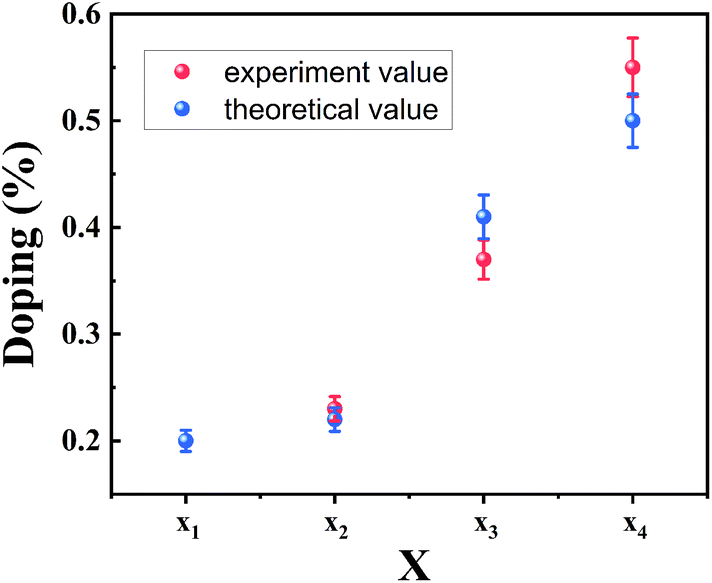
41 The calculated
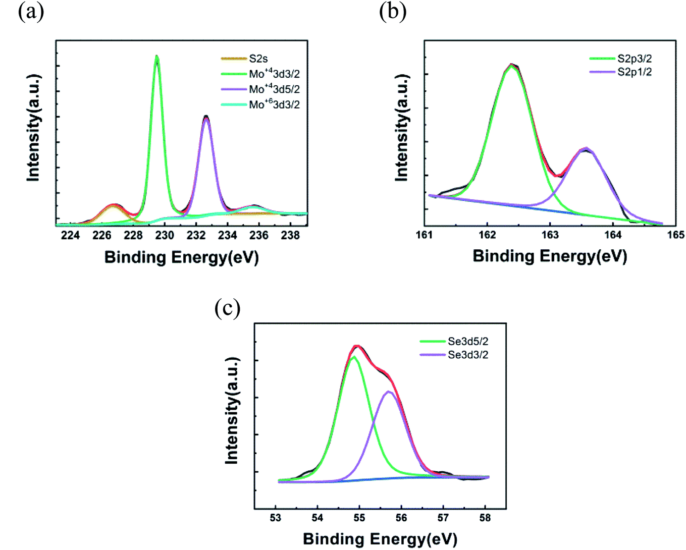
x values are approximately equal to 0.20, 0.22, 0.41 and 0.50. On the other hand, X-ray photoelectron spectroscopy (XPS) was adapted to characterize the chemical composition of crystals. In
Fig. 3, the XPS spectrum of as-grown MoS
2(1−0.37)Se
2(0.37) is displayed. The Mo 3d, S 2p, and Se 3d regions of the XPS spectra for MoS
2(1−0.37)Se
2(0.37) with different Se composition can be deconvoluted into various peaks. The Mo 3d window (
Fig. 3(a)) consists of Mo
4+ 3d5/2, Mo
4+ 3d3/2, Mo
6+ and S 2s, and the corresponding binding energies are 229.5, 232.6, 235.7 and 226.8 eV, which is in good agreement with the previous literature.
42 The presence of Mo
4+ 3d5/2, Mo
4+ 3d3/2 and S 2s is due to Mo 3d spin–orbit splitting in the formation of MoS
2 and MoSe
2. The reason for Mo
6+ in the energy spectrum may be the presence of MoO
3−xS
x in the reaction system. MoO
3−xS
x may be derived from incomplete vulcanization (or selenization) of metal Mo during the heating process, or it may be generated by the partial decomposition of MoS
2(1−x)Se
2x deposited during the cooling process. The S 2p doublet is shown in
Fig. 3(b), and it exhibits two peaks located at 162.4 eV and 163.6 eV, corresponding to S 2p3/2 and S 2p1/2 components, respectively. Further, as displayed in
Fig. 3(c), the Se 3d spectra can be deconvoluted into two peaks at 54.9 eV and 55.7 eV, corresponding to Se 3d3/2 and Se 3d5/2 components, respectively. The orbital binding energy diagram of S 2p and Se 3d with doping concentration is shown in Fig. S2.
† From the XPS results, we analyze the Se/S ratio by
eqn (2),
37| |
 | (2) |
where the
FS and
FSe are the relative sensitivity factors for S 2p3/2 (0.4453) and Se 3d3/2 (0.8493);
43 IS and
ISe represent the areas of the S and Se peaks. The Se content
x was estimated to be 0.20, 0.23, 0.37 and 0.55, corresponding to the Se/S ratios of 0.40
![[thin space (1/6-em)]](https://www.rsc.org/images/entities/char_2009.gif)
:
1.60, 0.46
:
1.54, 0.74
:
1.26 and 1.10
:
0.90, respectively. As compared with the
x value obtained from the bandgap (B exciton) by formula
(1), the XPS results are in good agreement with the theoretically calculated value, as displayed in
Fig. 4. The good agreement also indicates that the B exciton energy can be used to estimate the bandgap of bilayer MoS
2(1−x)Se
2x.
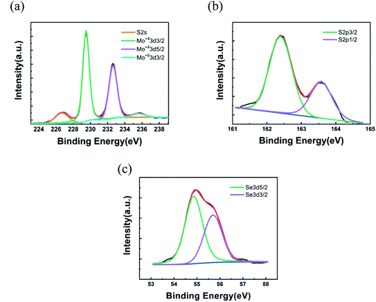 |
| | Fig. 3 XPS spectra of MoS2(1−0.37)Se2(0.37): (a) Mo 3d; (b) S 2p; (c) Se 3d. | |
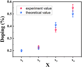 |
| | Fig. 4 Se composition of as-grown MoS2(1−x)Se2x by two methods. | |
In order to further understand the properties of bilayer MoS2(1−x)Se2x semiconductor alloy with different Se doping concentrations, we chose VASP (Vienna ab initio simulation package) for density functional theory (DFT) calculation and used the Perdew–Burke–Ernzerhof (PBE) functional to evaluate the band gap changes of the doped alloys.44 The 4 × 4 × 2 supercell was selected for the study of the pristine bilayer MoS2, which contains 96 atoms (32 Mo atoms and 64 S atoms). The side and top views of the atomic structure of MoS2(1−0.37)Se2(0.37) are shown in Fig. 5(a) and (b), respectively. MO, Se and S are represented by purple, green and yellow, respectively. The results of DFT calculation show that the bilayer MoS2 is an indirect band gap semiconductor with a band gap value of 1.70 eV, as seen in Fig. 5(c), which is consistent with a previous report.45 The direct bandgap of bilayer MoSe2 is 1.42 eV, which is lower than the 0.28 eV of bilayer MoS2. The band structures calculated at x = 0, 0.20, 0.37, 0.55 and 1 are shown in Fig. 5(d), and with the increase of Se doping content, the band gap value of bilayer MoS2(1−x)Se2x alloy has a decreasing trend corresponding to the PL spectrum shown in Fig. 2(b), but the band gap values are slightly lower than the experimental values. From the band structure theory, when Se enters the MoS2 lattice, the highest occupied molecular orbital (HOMO) and lowest unoccupied molecular orbital (LUMO) approach the Fermi level, resulting in band gap value decrease, which is a contraction of the band gap value.39 Compared with monolayer MoS2(1−x)Se2x alloy, the band bending effect of bilayer MoS2(1−x)Se2x alloy is more obvious,46 and the bilayer MoS2(1−x)Se2x alloy still shows the luminescence characteristic of direct band gap, which benefits the electronic structure research of 2D materials.
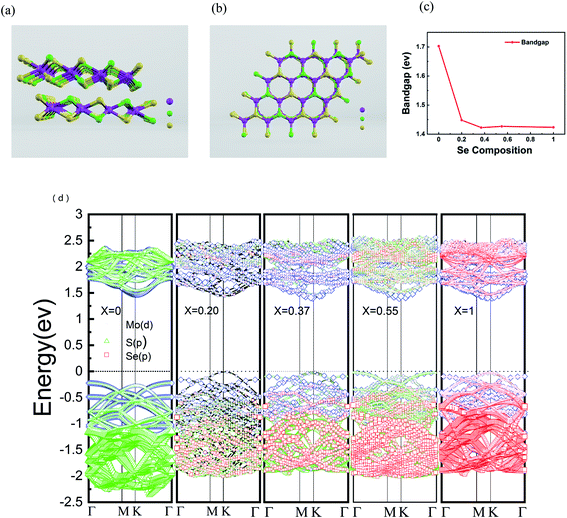 |
| | Fig. 5 (a and b) Side view and top view of the atomic structure of MoS2(1−0.37)Se2(0.37). MO, Se and S are represented by purple, green and yellow atoms, respectively. (c) Band energy of MoS2(1−x)Se2x when x = 0, 0.20, 0.37, 0.55, 1; (d) electronic band structure of bilayer Se-doped MoS2. | |
Conclusion
We have demonstrated an approach for preparing bilayer MoS2 using low-pressure chemical vapor deposition. Then, by introducing the Se component in the growth process of MoS2, MoS2(1−x)Se2x bilayers with various Se contents were synthesized. The formation of triangular-shaped microcrystals was confirmed by SEM, AFM, Raman, PL and XPS measurements. Because the MoS2 lattice is modified by Se doping, the grown alloys possess bandgaps between the values characteristic of bilayer MoS2 and MoSe2. The two sets of Raman modes and two PL peaks of bilayer MoS2(1−x)Se2x are consistent with the variation trend of the properties of monolayer MoS2(1−x)Se2x. Furthermore, we regard the B exciton energy as the bandgap of MoS2(1−x)Se2x ranging from 1.82 eV to 1.53 eV to estimate the x values, which is in good agreement with the XPS result. Additionally, we also use first-principles calculations to confirm the experimental results. With the addition of Se to bilayer MoS2 lattice, the band gap decreases. Changing of the Se/S ratio in growth crystals results in the band structure and bandgap adjustment, which provides a promising approach to produce 2D crystals with fancy properties in particular applications. The application of layered MoS2(1−x)Se2x could be further considered in later papers.
Conflicts of interest
There are no conflicts to declare.
Acknowledgements
This work was supported by the Fundamental Research Funds for the Central Universities (JB2019MS051, JB2015RCY03, JB2020MS042) and the National Natural Science Foundation of China (No. 91545122, No. 61704054).
References
- E. Fortin and F. Raga, Phys. Rev. B: Condens. Matter Mater. Phys., 1975, 11, 905 CrossRef CAS.
- W. Kautek, H. Gerischer and H. Tributsch, Cheminform, 1981, 12, 2471 Search PubMed.
- K. K. Kam and B. A. Parkinson, J. Phys. Chem. C, 1982, 86, 463 CrossRef CAS.
- S. J. Li, J. C. Bernède, J. Pouzet and M. Jamali, J. Phys. Condens. Matter, 1996, 8, 2291 CrossRef CAS.
- P. G. Moses, B. Hinnemann, H. Topsøe and J. K. Nørskov, J. Catal., 2007, 248, 188 CrossRef CAS.
- P. Grange and B. Delmon, J. Less Common Met., 1974, 36, 353 CrossRef CAS.
- C. T. Tye and K. J. Smith, Catal. Today, 2006, 116, 461 CrossRef CAS.
- Y. J. Wu, P. H. Wu, J. Jadczak, Y. S. Huang, C. H. Ho, H. P. Hsu and K. K. Tiong, J. Appl. Phys., 2014, 115, 193 Search PubMed.
- Y. Yoon, K. Ganapathi and S. Salahuddin, Nano Lett., 2011, 11, 3768 CrossRef CAS.
- J. Liu, Z. Zeng, X. Cao, G. Lu, L. H. Wang, Q. L. Fan, W. Huang and H. Zhang, Small, 2012, 8, 3517 CrossRef CAS.
- A. A. Tedstone, D. J. Lewis and P. O’Brien, Chem. Mater., 2016, 28, 1965 CrossRef CAS.
- P. Johari and V. B. Shenoy, ACS Nano, 2012, 6, 5449 CrossRef CAS.
- X. Hu, L. Kou and L. Sun, Sci. Rep., 2016, 6, 31122 CrossRef CAS.
- Z. m. Shi, Z. h. Zhang, A. Kutana and B. I. Yakobson, ACS Nano, 2015, 9, 9802 CrossRef CAS.
- Q. Zeng, H. Wang, W. Fu, Y. Gong and Z. Liu, Small, 2015, 11, 1868 CrossRef CAS.
- K. Zhou, N. Mao, H. Wang, Y. Peng and H. Zhang, Angew. Chem., Int. Ed., 2011, 50, 10839 CrossRef CAS.
- Q. Ma, M. Isarraraz, C. S. Wang, E. Preciado, V. Klee, S. Bobek, K. Yamaguchi, E. Li, P. M. Odenthal, N. Ariana, D. Barroso, D. Sun, G. v. S. Palacio, M. Gomez, N. Andrew, D. Le, G. Pawin, J. Mann, T. F. Heinz, T. S. Rahman and L. Bartels, ACS Nano, 2014, 8, 4672 CrossRef CAS.
- Q. Feng, N. Mao, J. Wu, H. Xu and L. Xie, ACS Nano, 2015, 9, 7450 CrossRef CAS.
- L. Yang, Q. Fu, W. Wang, J. Huang, J. Huang, J. Zhang and B. Xiang, Nanoscale, 2015, 7, 10490 RSC.
- G. Li, M. Q. Chen, S. X. Zhao, P. W. Li, J. Hu, S. B. Sang and J. J. Hou, Acta Phys.-Chim. Sin., 2016, 32, 2905 CAS.
- X. Ling, Y. H. Lee, Y. Lin, W. Fang and J. Kong, Nano Lett., 2014, 14, 464 CrossRef CAS.
- K. A. Kokh, V. V. Atuchin, T. A. Gavrilova, N. V. Kuratieva, N. V. Pervukhina and J. S. S. C. Surovtsev, Solid State Commun., 2014, 177, 16 CrossRef CAS.
- V. V. Atuchin, T. A. Gavrilova, T. I. Grigorieva, N. V. Kuratieva, K. A. Okotrub, N. V. Pervukhina and N. V. Surovtsev, J. Cryst. Growth, 2011, 318, 987 CrossRef CAS.
- V. V. Atuchin, S. V. Borisov, T. A. Gavrilova, K. A. Kokh, N. V. Kuratieva and N. V. Pervukhina, Particuology, 2016, 26, 118 CrossRef CAS.
- J. Chen, W. Tang, B. Tian, B. Liu, X. Zhao, Y. Liu, T. Ren, W. Liu, D. Geng, H. Y. Jeong, H. S. Shin, W. Zhou and K. P. Loh, Adv. Sci., 2016, 3, 1600033 Search PubMed.
- J. Xia, X. Huang, L.-Z. Liu, M. Wang, L. Wang, B. Huang, D.-D. Zhu, J.-J. Li, C.-Z. Gu and X.-M. Meng, Nanoscale, 2014, 6, 8949 RSC.
- H. S. S. R. Matte, A. Gomathi, A. K. Manna, D. J. Late and R. Datta, Angew. Chem., Int. Ed., 2010, 49, 4059 CrossRef CAS.
- A. R. Beal and H. P. Hughes, J. Phys. C Solid State Phys., 1979, 881 CrossRef CAS.
- H. Tang, K. Dou, C. C. Kaun, Q. Kuang and S. Yang, J. Mater. Chem. A, 2013, 2, 360 RSC.
- S. G. Pandya and M. E. Kordesch, Nanoscale Res. Lett., 2015, 10, 1 CrossRef CAS.
- Q. Gong, L. Cheng, C. Liu, M. Zhang and Y. Li, ACS Catal., 2015, 5, 2213 CrossRef CAS.
- H. Li, X. Duan, X. Wu, X. Zhuang, H. Zhou, Q. Zhang, X. Zhu, W. Hu, P. Ren and P. Guo, J. Am. Chem. Soc., 2014, 136, 3756 CrossRef CAS.
- S. Horzum, H. Sahin, S. Cahangirov, P. Cudazzo, A. Rubio, T. Serin and F. M. Peelers, Phys. Rev. B: Condens. Matter Mater. Phys., 2013, 87, 125415 CrossRef.
- A. Castellanos-Gomez, R. Roldán, E. Cappelluti, M. Buscema, F. Guinea, d. Z. Van, S. J. Herre and G. A. Steele, Nano Lett., 2013, 13, 5361 CrossRef CAS.
- G. Eda, H. Yamaguchi, D. Voiry, T. Fujita and M. Chen, Nano Lett., 2011, 12, 1 Search PubMed.
- K. F. Mak, C. Lee, J. Hone, J. Shan and T. F. Heinz, Phys. Rev. Lett., 2010, 105, 136805 CrossRef.
- V. Kiran, D. Mukherjee, R. N. Jenjeti and S. J. N. Sampath, Nanoscale, 2014, 6, 12856 RSC.
- Q. Feng, Y. Zhu, J. Hong, M. Zhang, W. Duan, N. Mao, J. Wu, H. Xu, F. Dong and F. Lin, Adv. Mater., 2014, 26, 2763 CrossRef.
- B. Rajbanshi, S. Sarkar and P. Sarkar, Phys. Chem. Chem. Phys., 2015, 17, 26166 RSC.
- M. Chhowalla, H. S. Shin, G. Eda, L. J. Li, K. P. Loh and H. Zhang, Nat. Chem., 2013, 5, 263 CrossRef.
- J. A. Wilson and A. D. Yoffe, Adv. Phys., 1969, 18, 193 CrossRef CAS.
- J. Kang, S. Tongay, J. Li and J. Wu, J. Appl. Phys., 2013, 113, 10451 Search PubMed.
- S. Umrao, J. Jeon, S. M. Jeon, Y. J. Choi and S. Lee, Nanoscale, 2017, 9, 594 RSC.
- W. Zhang, X. Li, T. Jiang, J. Song, Y. Lin, L. Zhu and X. Xu, Nanoscale, 2015, 7, 13554 RSC.
- S. Andrea, L. Sun, Y. Zhang, T. Li and J. Kim, Nano Lett., 2010, 10, 1271 CrossRef.
- Q. Feng, Y. Zhu, J. Hong, M. Zhang, W. Duan, N. Mao, J. Wu, H. Xu, F. Dong and F. Lin, Adv. Mater., 2014, 26, 2763 CrossRef.
Footnote |
| † Electronic supplementary information (ESI) available. See DOI: 10.1039/d0ra07776c |
|
| This journal is © The Royal Society of Chemistry 2020 |
Click here to see how this site uses Cookies. View our privacy policy here. 
 Open Access Article
 This Open Access Article is licensed under a Creative Commons Attribution-Non Commercial 3.0 Unported Licence
 ab,
Fangchao Luab and
Wenjie Wang
ab,
Fangchao Luab and
Wenjie Wang