
 Open Access Article
 This Open Access Article is licensed under a
 Creative Commons Attribution 3.0 Unported Licence
ZnO nanostructured materials for emerging solar cell applications
Arie Wibowo *ab,
Maradhana Agung Marsudia,
Muhamad Ikhlasul Amalc,
Muhammad Bagas Anandaa,
Ruth Stephaniea,
Husaini Ardya and
Lina Jaya Diguna*d
*ab,
Maradhana Agung Marsudia,
Muhamad Ikhlasul Amalc,
Muhammad Bagas Anandaa,
Ruth Stephaniea,
Husaini Ardya and
Lina Jaya Diguna*d
aMaterial Science and Engineering Research Group, Faculty of Mechanical and Aerospace Engineering, Institut Teknologi Bandung, Jl. Ganesha 10, Bandung, 40132, Indonesia. E-mail: ariewibowo@material.itb.ac.id
bResearch Center for Nanoscience and Nanotechnology, Institut Teknologi Bandung, Jl. Ganesha 10, Bandung, 40132, Indonesia
cResearch Center for Metallurgy and Materials, The Indonesian Institute of Sciences, Puspitek, Serpong, Banten 15314, Indonesia
dDepartment of Renewable Energy Engineering, Universitas Prasetiya Mulya, Kavling Edutown I.1, Jl. BSD Raya Utama, BSD City, Tangerang 15339, Indonesia. E-mail: lina.diguna@prasetiyamulya.ac.id
First published on 24th November 2020
Abstract
Zinc oxide (ZnO) has been considered as one of the potential materials in solar cell applications, owing to its relatively high conductivity, electron mobility, stability against photo-corrosion and availability at low-cost. Different structures of ZnO materials have been engineered at the nanoscale, and then applied on the conducting substrate as a photoanode. On the other hand, the ZnO nanomaterials directly grown on the substrate have been attractive due to their unique electron pathways, which suppress the influence of surface states typically found in the former case. Herein, we review the recent progress of ZnO nanostructured materials in emerging solar cell applications, such as sensitized and heterojunction architectures, including those embedded with promising perovskite materials. The remarkable advancement in each solar cell architecture is highlighted towards achieving high power conversion efficiency and operational stability. We also discuss the foremost bottleneck for further improvements and the future outlook for large-scale practical applications.
1 Introduction
Emerging solar cell technologies that use complex and advanced materials, such as perovskite, dye-sensitized, organic, quantum dot and multijunction, were born to answer the challenges for conversion efficiency and durability. None of the developed solar cell technology has closely achieved the theoretical energy conversion limit to 90%. The primary cause of the inefficiency of solar cells is related to the energy bandgap, as well as the transmission and thermalization losses. This is strongly related to the properties of the active material, including their defects. In addition, the intrinsic stability of these materials affects the lifetime or durability of the solar cells systems. The desired properties of the charge transport materials for solar cells application are ideal energy levels that correspond to the high absorption efficiency of the solar spectrum, high carrier mobility, good conductivity, and efficient extraction of the excited carriers.ZnO materials, one of the group II–VI binary compound semiconductors, have been considered in solar cell applications due to their stability, high conductivity, high electron affinity and excellent electron mobility. Fig. 1 illustrates the advantages of ZnO as an active material for solar cell applications. ZnO materials are wide bandgap semiconductors with a band gap of 3.1–3.3 eV that absorb light only in the UV region. ZnO can also be coupled with smaller energy gap materials, such as dye sensitizers, organic polymers, and smaller band gap semiconductors, to extend their light absorption to the visible region. The bulk ZnO has been reported to have an exciton Bohr radius (aB) of 2.34 nm.1 This is comparable to the significant confinement effects, experimentally observed for the solution phase synthesized ZnO particles with the particle radii of less than about 4 nm, due to the relatively small effective masses for ZnO, i.e., me = 0.26m0, mh = 0.59m0 and m0 is the free electron mass.2 The high electron mobility of ZnO makes this material attractive for solar cell application, 205–300 for bulk3,4 and 1000 cm2 V−1 s−1 for nanorod ZnO.5 These values are relatively high compared to those of the commonly used TiO2, i.e., 0.1−4 cm2 V−1 s−1.6 Moreover, the electron diffusion coefficient is 5.2 for bulk and 1.7 × 10⁻⁴ cm2 s−1 for the nanoparticulate film ZnO.7 Conversely, in the bulk and nanoparticulate film TiO2, the electron diffusion coefficient becomes 0.5 and 10−8−10−4 cm2 s−1, respectively.8 ZnO is also well-known as a polymorph, having a different type of structure depending on the synthesis method. The nanomorphology of ZnO comprise nanospheres, nanowires, nanorods, nanoflower, nanotubes, nanocrystals, and 3D nanostructures (core–shell). These excellent attributes have made ZnO widely applied in many areas, such as sensors, surface coating, porous ceramics, photodetectors, nano-piezoelectric, and supercapacitors, in addition to solar cells. There are also many available methods to prepare ZnO nanomaterials from different pathways (biological/physical/chemical), such as green synthesis using microorganisms, hydrothermal, sol–gel, electrochemistry, inkjet printing, atomic layer deposition, and sputtering technique.
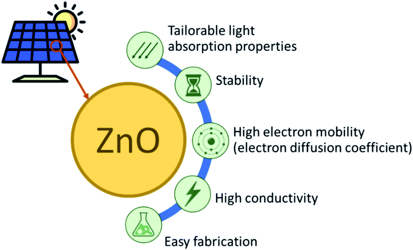 | ||
| Fig. 1 The merits of ZnO for solar cell application. | ||
In this review, the latest application of ZnO in third-generation solar cell technologies is thoroughly discussed. Different solar cell architectures, i.e., sensitized solar cells and heterojunctions solar cells, including those embedded with promising perovskite materials, will be reviewed in accordance with the influence of the synthesis strategies on the ZnO properties. These approaches include the application of different nanostructures of ZnO, deposition and post-treatment method, and inclusion of dopant materials (Fig. 2). The discussion will be concluded by the proposal of future strategies to improve the current achievements Fig. 2.
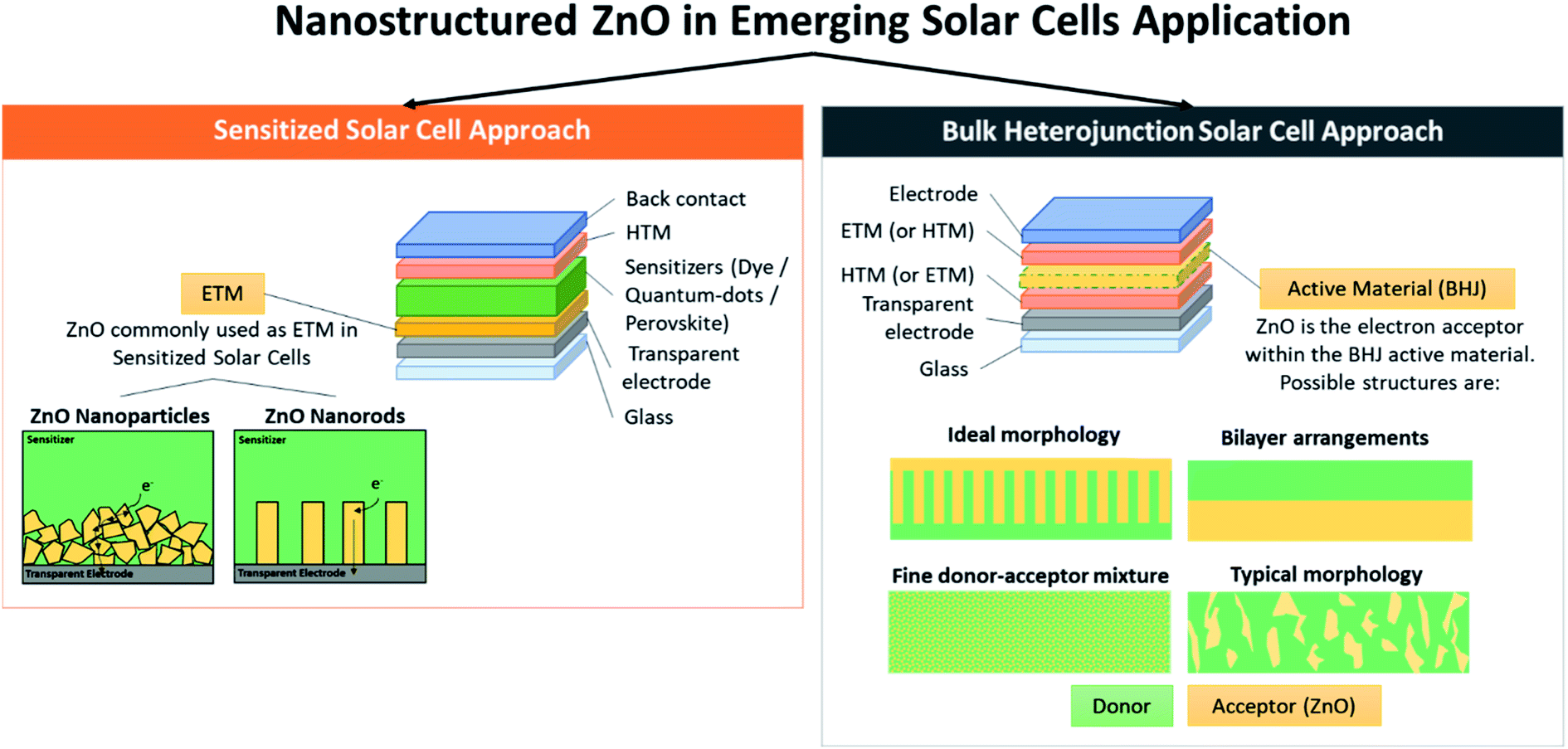 | ||
| Fig. 2 Nanostructured ZnO in emerging solar cell applications. | ||
2 Emerging solar cell application
2.1 Sensitized solar cells
Dye-sensitized solar cells (DSSCs) were first proposed by O'Regan and Grätzel in 1991, and have attracted great interest as an alternative to conventional silicon solar cells. The fabrication is straightforward and low-cost, with good long-term stability and energy conversion efficiency exceeding 10%.9 Ru-based dyes are utilized as photosensitizers that are attached to the mesoporous metal oxide photoelectrode with large surface areas, and absorb solar energy efficiently. The electrons injected by the optically excited dye into the metal oxide conduction band diffuse across the semiconductor film layer, and reach the back contact. Redox couples diffuse in solution, which are in turn reduced at the counter electrode, and regenerate the oxidized dye. Because of the sensitizers, the high expense to provide the typical dyes (N3, N719) has encouraged the alternative use of narrow band gap semiconductor quantum dots (QDs), owing to their size-tunable optical properties to match the solar spectrum. Moreover, QD-sensitized solar cells (QDSCs) have the capability of producing multiple electron–hole pairs per photon quantum yields greater than 1 through impact ionization.10–12 In the early studies, QD-sensitized solar cells showed performances well below the expectation, where the achieved efficiency in two-electrode configurations was below 1%.13,14 Later, the efficiency of 2.7% reported by Diguna et al. in 2007 brought about a resurgence in the development of QDSCs.15 The different morphologies of the photoanode have also been considered to enhance the light-harvesting efficiency, such as the inverse opal due to its large interconnected pores for better penetration of the dye and photon confinement at a wavelength near the photonic band gap for the significant enhancement of dye absorption.16 In the following sections, the application of various ZnO-nanostructured materials and their recent progress in DSSCs, PSSCs, and QDSCs are discussed in detail.The traditional nanoparticle film in DSSCs effectively provided a large surface area for the adsorption of light-harvesting dye molecules. However, the electron transport through the nanoparticle film was based on trap-limited diffusion, a slow mechanism that limited the device efficiency, especially at longer wavelengths. Therefore, an array of oriented 1D nanostructures, such as nanowires, nanorods and nanotubes, was later introduced as a promising solution to increase the electron diffusion length in the anode. The aspect ratio (length divided by diameter) of the nanowires may be up to 1000, while that of the nanorods is much smaller, usually less than ten depending on the synthesis method and condition. In 2005, the ZnO nanowire photoanode with an array length between 20–25 μm and a surface area of up to one-fifth of a nanoparticle film was synthesized using a seeded growth process. The ZnO quantum dots as a 10–15 nm thick film was initially deposited onto the FTO substrate by dip coating. Later, wires were grown from these nuclei through thermal decomposition of the zinc complex. With the sensitization of the ruthenium dye, it demonstrated 1.5% efficiency at one sun.26 In the same studies, the electron injection from the photoexcited ruthenium dyes into nanowires and nanoparticles was evaluated by using femtosecond transient absorption spectroscopy. The resulting bi-exponential kinetics of the nanowires (time constants of <250 fs and around 3 ps) confirmed the faster electron injection relative to the nanoparticles with a tri-exponential response (time constants of <250 fs, 20 ps and 200 ps). The Core-shell concept was then applied to the ZnO nanowire photoanode by coating ZnO nanowires with the thin shell of amorphous Al2O3 or anatase TiO2 by atomic deposition.27 A very thin alumina shell acted as a tunnel barrier that improved the Voc by impeding recombination, but blocked electron injection as it became thicker. On the contrary, titania shells were found to suppress the rate of recombination and improve the open-circuit voltage and fill factor, in which the shell thickness of 10–25 nm caused a dramatic increase in efficiency by up to 2.25% under one sun.
The photovoltaic properties of the ZnO nanorods were reported to be dependent on not only the rod size, but also on their orientation.28 Vertically aligned ZnO nanorods with N179 sensitization exhibited very low power conversion efficiency, i.e., 0.22% and 0.09% for hydrothermally grown and vapor deposited ∼3.5 μm-length ZnO nanorods.29 Modification on the ZnO nanorod surface with gold nanoparticles formed a Schottky barrier, and then blocked the electron transfer back from ZnO to the N719 dye and electrolyte, thus increasing the efficiency up to 1.2%.30 Doping the ZnO nanorods with Al also improved the performance of the N719-sensitized ZnO nanorods from 0.05% to 1.34%.31 Here, the occupation of the trivalent Al3+ in the divalent Zn2+ ion site increased the electron concentration and thus the electrical conductivity, allowing electrons to move easily into the Al-doped ZnO conduction band. Chemically etching the center part of the electrochemically deposited ZnO nanorods produced a ZnO nanotube array. The employment of the 5.1 μm-length ZnO nanotube as a photoanode with N719 sensitization showed an efficiency of 1.18%.32 On the other hand, ZnO nanotube photoanodes templated by an anodic aluminium oxide exhibited an efficiency of 1.6% under AM 1.5 illumination.33 Combined with atomic layer deposition to conformally coat the nanotube pores, the design could provide a direct path for charge collection over tens of micrometers thickness, indicated by the exceptional photovoltage of 739 mV and fill factors of 0.64. Unfortunately, the low photocurrent caused by insufficient light harvesting due to the small roughness factor and photoanode reflectivity/scattering (light coming from the counter electrode side) limited the overall efficiency. The increase of the surface area was required to further improve the energy conversion efficiency.
The dye in DSSCs also plays a critical role in enhancing the PCE. A compatible dye in the ZnO-based DSSCs will improve the electron injection efficiency. The enhancement of the electron injection efficiency depends on the electronic coupling and relative energy levels between the dye and the semiconductor, the lifetime of the dye, and ultimately on the density of the electron-accepting state (DOS) in the semiconductor. The electronic coupling between the dye and semiconductor relies on the selection of the dye group for the appropriate semiconductor. The dyes shall be identified or synthesized, for which the LUMO (Lowest Unoccupied Molecular Orbital) and HOMO (Highest Occupied Molecular Orbital) levels match, respectively, with the conduction band energy levels and the valence band energy levels of the semiconductor. The lifetime of the excited state is a fundamental property of the photosensitizer. The dye with longer life in the excited state is expected to be easier for charge transfer.34
In contrast to TiO2, ZnO is not compatible with the Ru dye due to its more alkaline nature, making it susceptible to low pH conditions. The Ru dye also removes Zn2+ ions from the ZnO lattice. The improper immersion duration of the ZnO film in the ruthenium dye could lead to a lower efficiency for the DSSC due to ZnO film release, reduction in the number of free electrons, promotion of the recombination process, and transformation of the porous film to a denser one.34,35 In some recently reported research studies (Table 1), metal-free dyes such as indoline dyes, D205 and D149,36 heptamethine-cyanine dye (KFH-3),37 C220,38 carbazole dyes,39 anthocyanins,40 and Xanthenes41 were found to be the right-choice for this purpose. Recent studies by Chang et al. and Lin et al. have shown that dyes with relatively lower acidity (indoline dye coded D149) show a relatively good compatibility with ZnO. Both types of research studies conducted found that an efficiency higher than 5% can be achieved for the flexible ZnO-based DSSC.42,43
| ZnO nanostructure | Dye | Doping | PCE (%) | Ref. |
|---|---|---|---|---|
| Nanorods | Crystal violet | La | 0.36 | 49 |
| Nanoflower | N719 | Li | 1.23 | 48 |
| Nanoparticles | Mercurochrome | Ag | 2.02 | 47 |
| Nanospheres | N719 | In | 2.7 | 51 |
| Hollow spheres | N719 | — | 3.28 | 53 |
| Nanorods | N719 | — | 3.75 | 54 |
| Nanoparticles | N719 | Iodine | 4.01 | 45 |
| D205 | 4.44 | |||
| Pomegranate | N719 | — | 4.35 | 53 |
| Nanoparticles | CYC-B1 | — | 5.4 | 55 |
| Nanosheets | N3 | B | 6.75 | 46 |
In a more recent study, several efficient metal-free organic sensitizers were developed by Selopal et al. called B18, BTD-R, and CPTD-R for ZnO-based DSSCs. The B18 dye provides better photovoltaic properties than the other two dyes in the hierarchically structured ZnO and commercial TiO2 due to the higher electron injection potential and better light harvesting. The TCD/TVD results showed that the device with dye B18 had a better τR and negligible shift in dye-sensitive photoanode CB compared to the CPTD-R and BTD-R dye-based devices.44
Another way to improve electron transport in the Zn photoanode, which also enhances cell efficiency, is to add dopants to the ZnO film. Dopants will fill the holes in the cell, thus increasing the recombination injected electron in the semiconductor.34 Several materials such as iodine,45 B,46 Ag,47 Li,48 La,49 Sr,50 In,51 and Nd52 could be doped into the semiconductor film of ZnO, according to some reports. Zhao et al. used iodine-doped ZnO-based as a photoanode in dye-sensitized solar cells with indoline D205 and N719 as the sensitizers. The result demonstrated that iodine-doping boosts the efficiencies compared to the cells without iodine. The efficiencies of the D205-I-ZnO based DSSC and N719-I-ZnO based DSSC were enhanced by 20.3% and 17.9%, respectively.45 Mahmood and Park reported a cell fabricated with ZnO nanosheets doped with boron and using the N3 dye as a sensitizer, achieving a significant enhancement in PCE (6.75%) in contrast to the undoped ZnO nanosheets (2.62%) and BZO films only including nanosized crystallites (3%).46 The work from Lanjewar et al. revealed that upon doping with Ag, the band gap is sharply reduced and the resulting Ag:ZnO photoelectrode could absorb the visible light range to a great extent. The most massive reduction in the band gap was achieved from 3.28 eV for the pure ZnO film to 2.65 eV for Ag:ZnO with 10.3 wt% doping with the enhancement of PCE from 0.55% to 2.02%.47 In a very recent study, Aksoy and collaborator investigated the addition of Li into ZnO powder using N719 dye for dye-sensitized solar cells. The result suggested that the nanoflower morphology was formed, and the efficiency of the cells rise to the value of 1.23%. The enhanced efficiency was associated with the change in the morphology, and an improvement in the crystallinity in Li-doped ZnO based DSSCs.48 Research conducted by Goel and co-worker demonstrated that the La-doped ZnO-based nanopowder solar cell exhibited superior photovoltaic performance when compared to the pure ZnO-based cell. The light harvesting efficiency (η) increased from 0.20% to 0.36% on doping with La.49 In a study by Chava et al. using Indium-doped ZnO, the maximum photoconversion efficiency of 2.7% was achieved on 0.2 In–ZnO photoelectrode films that consisted of nanosized crystallites and aggregated spheres of nano-crystallites.
The enhancement in the performance of DSSCs with 0.2 In–ZnO films was attributed to the strong light scattering phenomenon of aggregated spheres within the photoelectrode film, the pore size of the aggregates, which offers a more porous structure for dye infiltration and electrolyte diffusion.51
Different ZnO structures have also been pursued to achieve specific features, such as better electron transport than those obtained in nanoparticles. One-dimensional (1D) structures such as nanorods, nanowires, and nanotubes, had vertically aligned electrical pathways and reduced particle-to-particle hopping of electrons usually found in the nanoparticle network, which are expected to increase the efficiencies of those photoelectrical devices. Modification on the ZnO nanorod, i.e., taper-like arrays, could minimize the charge transfer resistance, thus increasing the short current circuit and conversion efficiency consequently for the case of nitrogen-doped graphene QDs.62 Moreover, the efficiencies of the ZnO nanorod array devices are limited by their low light-harvesting ability. Nanotubes have a larger surface area than nanorods of similar length and diameter. ZnO nanotube arrays have been proved to have a superior ability as compared with ZnO nanorod arrays due to the excellent light scattering efficiency on account of their 1D tubular nature.63 Taking into account the critical role of the QDs interfaces in carrier relaxation,64 interfacial engineering (such as surface modification) has reported over one decade in suppressing surface defects, leading to smooth electron transfer and thus improving the photovoltaic performance of the QD-sensitized TiO2 solar cells.15,56,58 The similar approach has also been introduced on the CdS/CdSe quantum dot co-sensitized ZnO photoanode by MnS passivation layer to suppress charge recombination at the photoelectrode/electrolyte interface, and also enhance the light-harvesting capability in terms of both absorbance intensity and absorption range.65 One option to increase the solar cell performance is by structure architecture, enabling the light scattering and thus, the light-harvesting efficiency. ZnO hollow microspheres have been found to generate light scattering and thus improve the power conversion efficiency of the ZnxCd1−xSe QDSSC.66 On the other hand, this hollow structure may also lead to the defects located at the surface. To tackle this issue, the TiO2 passivation layer on the hollow microsphere surface has been reported recently to improve the CdSe/CdS QDSSC performance. The improvement not only produced better light harvesting, but also reduced the charge recombination and lengthened the electron lifetime.67 QDs have a unique capability of producing multiple electron–hole pairs per photon quantum yields greater than 1 through impact ionization.10,11 The attachment of QDs on the ZnO surface has been reported to possibly speed up carrier relaxation in the QDs, which is an essential factor for hot-carrier energy harvesting via multiple electron generation and hot electron transfer, depending on the exact linker molecules.68 Although an external photocurrent quantum efficiency of more than 100% has been reported for the hererojunction ZnO/PbSe QD solar cell,69 to the best of our knowledge, there are no reports on QDSSCs yet.
Besides the design of the photoanode in terms of its semiconductor properties, interfaces and crosslinking molecules, the redox couples and counter electrodes used should also be considered carefully for higher photoconversion efficiency to ensure a smooth interfacial charge transfer at the photoanode/electrolyte and electrolyte/counter electrode. Relative to the commonly used iodide/triiodide (I−/I3−) redox couple and platinum counter electrode in dye-sensitized solar cells (DSSCs), the sulphide/polysulphide redox couple and CuS counter electrode have been proposed to be suitable for metal chalcogenide (e.g., CdSe)-based QDSSCs, respectively.56,58,64 The presence of Sn2− (oxidized counterpart) in the sulphide redox couple causes the quick scavenging of the photogenerated hole in the CdSe QDs by the redox couple, and thus regenerating QDs. However, the greater concentration of polysulfide also contributes the back electron transfer process.70 Leakage of the liquid electrolyte unfortunately results in a medium loss for charge transfer. Thus, solid-state electrolytes might be considered, such as polysulfide integrated polyvinylpyrrolidone.71 On the other hand, the penetration of solid electrolyte in the entire photoanode still is a challenging issue to be tackled. ZnO has also been applied for the counter electrode, in which the metal sulfide (e.g., CuS, PbS)-deposited ZnO nanorod counter electrode has shown better electrocatalytic activity than CuS (Table 2).72,73 The strategies to improve QDSSC performances by using ZnO nanostructured materials are summarized in Table 2.
| Photoanode | Approach | QD | Isc (mA cm−2) | Voc | Ff | η (%) | Ref. |
|---|---|---|---|---|---|---|---|
| Ultrasonic spray pyrolysis-synthesized ZnO | Good contact between ZnO/FTO or ZnO/QD | CdS | 6.99 | 0.66 | 0.33 | 1.54 | 59 |
| ZnO nanotaper | Tapering morphology on nanorod | Nitrogen-doped graphene | ∼1.04 | — | — | ∼1.15 | 62 |
| ZnO nanotube | Vertically aligned electrical pathways, light scattering | CdSe | 2.09 | 0.44 | 0.41 | 0.44 | 63 |
| ZnO hollow microspheres | Light scattering | ZnxCd1−xSe | 20.77 | 0.43 | 0.33 | 2.95 | 66 |
| ZnO hollow microspheres/TiO2 passivation layer | Light scattering, reduced surface defects | CdSe/CdS | 14.64 | 0.46 | 0.47 | 3.16 | 67 |
| ZnO mesoporous nanoparticles | Reduced surface defects and enhanced light harvesting capability | CdS/CdSe/MnS passivation layer | 13.74 | 0.6 | 0.44 | 3.7 | 65 |
| ZnO nanorods | CuS/ZnO nanorods counter electrode | Cds/CdSe | 14.48 | 0.76 | 0.38 | 4.18 | 72 |
| TiO2 nanoparticles | PbS/ZnO nanorods counter electrode | CdS/CdSe/ZnS | 13.28 | 0.633 | 0.566 | 4.76 | 73 |
| ZnO nanowire | Minimizing the SeO2 layer on CdSe QDs | CdSe/CdS | 16.0 | 0.72 | 0.41 | 4.8 | 61 |
In addition to pursuing high photoconversion efficiency, the design of the assembly process (including materials used for sealing) is a limiting factor for long-term stability in a real application, even though it may not directly affect the performance. Extensive evaluation under various conditions, such as thermal, light and humidity stresses, should also be carried out to determining its stability. Afterward, the appropriate architecture and engineering of QDs-sensitized solar cells should be done comprehensively to make its practical application more feasible.
n-Type semiconductor oxides (such as TiO2, ZnO) are widely used as electron-transporting materials (ETMs) to extract and transport the photogenerated electrons. At the same time, they block the photogenerated hole to suppress charge recombination in perovskite bulk films.80,81 Considering their crucial role in the photovoltaic performance of PSCs, it is essential to control the characteristics of ZnO as the ETM layer, especially its morphology, interfacial properties, trap states, and energy level alignment.82
2.1.3.1 Influence of the ZnO nanostructure. Variations in the nanostructures have a significant impact on three aspects of the perovskite films: (i) the perovskite layer morphology and loading, (ii) the quality of the ZnO/perovskite interface, and (iii) the quality of the perovskite itself.81 In other words, ZnO with different nanostructures will lead to other PSC performances by affecting the perovskite directly, which will define the resulting PCE of a PSC. Briefly, the one-dimensional nanostructured ZnO (i.e., nanorods; NRs) showed better performances than ZnO nanoparticles (NPs). These results can be observed mainly due to the single crystal one-dimensional structures of ZnO provides direct electron pathways for the electronic transport in PSCs.80 On the other hand, electrons suffer many trapping-detrapping events in NPs structures, especially at the grain boundaries that slow down the electron transfer.83–85 However, the trend cannot be linearly determined as there are other factors affecting PCE, besides the interacting properties of the perovskite and ETM in PSCs.
2.1.3.2 Influence of ZnO deposition and post-treatment method. Variations in the ZnO processing method may affect the interaction between the perovskite and ETM, which determines the overall PCE of the PSCs. Zheng et al.86 showed that ZnO NPs deposited using the spin coating method resulted in a low power conversion efficiency (PCE) due to the formation of a pinhole-surface that creates the defective interface, leading to a loss of carriers.86 The PCE of the PSCs could be increased by adding the post-treatment method on the prepared ZnO NPs. Duan et al. showed that the addition of the in situ thermal decomposition on the spin-coated ZnO was able to change the morphologies of ZnO from nanoparticles to interconnect the net-like structure, leading to a power conversion efficiency increase to 13.1%.87 A higher PCE could be acquired by using ZnO NR. Theoretically, NR can result in better PCE by providing a direct electron pathway with its one-dimensional structure. To improve the PCE even more, Mahmood et al.88 improved the conventionally low aspect-ratio (LAR) ZnO NR by directly introducing the PEI polymer as a capping agent during the hydrothermal growth process, which resulted in a high aspect-ratio (HAR) ZnO NR. This modification increases the PCE as NR with a large diameter, hindering the perovskite infiltrations in the ETM and resulting in an increase of PCE from 10.3% to 11.5%. An even higher PCE can be achieved by passivating the ZnO NR layer with Al2O3, along with the post-treatment of solvent-annealing in ethanol vapor. This particular method increases the carrier diffusion length, as well as the recombination resistance in PSCs, which can result in 17.3% efficiency.89
2.1.3.3 Influence of dopants and doping for interface engineering. More improvements of a PSC device can be achieved by improving the ZnO electronic properties for ETM by doping. Doping is already known to be adequate in modifying the electronic properties of metal oxide semiconductors.90 The doping can also significantly affect the morphology of ZnO, and is usually used to increase the free charges and thus, conductivity in solar cells.81 In the case of ZnO, doping can be achieved by either replacing the Zn2+ cation or the O2− anion. Cationic dopants are typically metals, whereas anionic dopants are non-metals. Replacing Zn2+ by a different cation is expected to affect the conduction band (CB) structure. The upper edge of the valence band (VB) consists of O2− 2p bands and replacing O2− with a different anion affects the VB energy. Therefore, the doping of ZnO can shift the Fermi level (EF) in the direction of the CB, which helps increase the conductivity and facilitate the work function.81,91
In the case of using ZnO, several studies have shown the success in doping ZnO for PSC application. Dopants, such as N,88 I,92 Al,93 Ga,94 and Mg,95 are the highly preferred n-type dopants for ZnO films. The work of Mahmood et al.88 achieved 16.1% PCE by altering the aspect-ratio of the ZnO NR, and also by doping ZnO with electron-rich nitrogen, which was proven to efficiently increase the conductivity of the oxide layer, reduce the internal resistance, and hence increase the electron density of the ETM. Zheng et al. reported iodine-doped ZnO as ETM.92 Through the treatment of introducing iodine, the usual hydrothermal process resulted in a wide-hexagonal-structure of ZnO:I nanopillars, making a compact and even planar ZnO:I thin film surface with few voids compared to ZnO NR arrays. Iodine-doping to ZnO also promotes an electron extraction from the perovskite layer by a more favourable work function of the ETM, leading to a PCE as high as 18.24% of the device. Al-doped ZnO (AZO) and Ga-doped ZnO (GZO) films are also excellent candidates for transparent conducting oxide materials because they are inexpensive, have suitable ionic radii, and show excellent optical transmission performance. The work of Mahmood et al.93 showed that Al doping could greatly enhance the carrier concentration and electron mobility of pure ZnO, which results in superior conductivity. In addition to that information, Dong et al.96 worked to improve ZnO NR by Al-doping, making AZO. The resulting Al-doped ZnO (AZO) is reported to have a higher conduction band, a higher electron mobility, and a higher electron density than ZnO. The study shows that the use of AZO resulted in an increase of the solar cell efficiency from 8.5% to 10.07%, making them the first to fabricate the highly efficient Al-doped ZnO nanorod-based PSCs (Table 3). Summary of several factors that affect to photovoltaic performance of MAPI-based PSCs is presented in Table 3.
| ZnO nanostructure | ZnO preparation and/or post treatment method | Doping element | PCE (%) | Ref. |
|---|---|---|---|---|
| Nanoparticles | Non-aqueous preparation | 4.3 | 97 | |
| Nanoparticles | Spin-coating | 7 | 98 | |
| Nanorods | Spin-coating | 9.1 | 99 | |
| Nanorods | Spin-coating | Al | 10 | 96 |
| Nanorods | LAR nanorods | 10.3 | 88 | |
| Nanorods | Hydrothermal self-assembly + interfacial defect passivation (atomic layer deposition of Al2O3 monolayers on the ZnO nanorods) | 10.4 | 100 | |
| Nanoparticles | ZnO/ZnS core–shell structure, spin-coating | 10.9 | 86 | |
| Nanoparticles | Spin-coating, followed by in situ thermal decomposition | 13.1 | 87 | |
| Nanorods | HAR nanorods | 11.5 | 88 | |
| Nanorods | LAR nanorods | N | 11.6 | |
| Nanorods | HAR nanorods | N | 13.6 | |
| Nanorods | Hydrothermal process | Mg | 15.3 | 95 |
| Nanorods | Introducing PEI as capping agent, HAR | N | 16.1 | 88 |
| Nanorods | ZnO NR Al2O3 passivation + solvent-annealing | 17.3 | 89 | |
| Nanorods (nanopillars) | Hydrothermal process | I | 18.2 | 92 |
| Nanoparticle | Two-step radio-frequency magnetron sputtering | Ga | 20.2* | 94 |
A study by Chen et al.94 showed that doping ZnO NR with Ga increased the carrier concentration such that an even higher power conversion efficiency of 20.167% was obtained, with an exciting transmittance value of >87% in the range of 0.4–1.2 μm. Dong et al.95 also worked to make Mg-doped ZnO, which is supposed to restrain the charge recombination in PSCs, owing to the conduction band offset at the ZnO/perovskite absorber interface, which increases the device efficiency.
Besides improving the ZnO properties, doping can also improve the PSC performance by simultaneously enhancing the interface interaction between the perovskite and the ZnO, in other words: interface engineering. This is because the charge generation, separation, collection, and recombination mainly occur at the interfaces. Interface engineering would be necessary to lower the interfacial energy barriers for charge transport, to suppress charge recombination, and to improve the performance of the solar cell.15 For example, iodine-doping to ZnO resulted in a lower work function for efficient electron extraction from the perovskite into ZnO:I. This was achieved by reducing the photoluminescence decay life-time, which is favourable for inhibiting the charge recombination at the interface, leading to a remarkable enhancement of Jsc and FF, together with PCE.92 Iodine-doping to ZnO also enables a better electrical contact interface between the perovskite and ZnO:I for facile charge transport, which effectively prevents charge accumulation at the interfaces.92 The study made by Dong et al.,101 which improved ZnO to make AZO, was shown to improve the material as an ETM. It also indicates that the use of this compound could reduce the recombination at the ZnO NR/perovskite interface. Ga-doped ZnO was also shown to have a crater-textured surface structure that can increase the contact area between ETM and perovskite, which reduces the contact resistance and increases the transmission channel of the electrons.94 The Ga doping in ZnO could increase the carrier concentration that makes the electrons effectively fill the interface traps and decrease the interface trap density, which was beneficial for reducing the electron capture and preventing carrier recombination at the interface, and improving the electron transporting efficiency from the perovskite to ETLs. Doping Mg to ZnO was also shown to raise the conduction band offset (ΔEC) at the ZnO/perovskite interface, suppressing the charge recombination, leading to improvements in cell performance.95
2.2 Heterojunction solar cells
One of the most commonly found fully inorganic heterojunction solar cells consists of a mix between ZnO and lead chalcogenides (PbX; e.g., PbS, PbSe, PbTe). PbX has emerged as an excellent material for photovoltaic devices, as it has a uniquely large dielectric constant and therefore large Bohr radii, thus resulting in a significant quantum confinement effect.104 The energy level of PbX also favors combination with ZnO, in which the LUMO of the PbX can be tuned to minimize the difference with the conduction band energy of ZnO. Leschkies et al. reported a heterojunction solar cell based on the planar heterojunction between the PbSe nanocrystals and ZnO thin film.105 Compared to the Schottky solar cell made with similar PbSe NCs, the heterojunction solar cell utilizing the ZnO thin film features larger photocurrents and Voc value, with an overall power conversion efficiency (PCE) of 1.6%. They found out that the thermal annealing of ZnO (up to 450 °C) yields a positive effect on the electrical conductance and electron mobility of the ZnO film due to the reduced defects in the post-annealed ZnO. To increase the efficiency, they proposed the utilization of nanostructures instead of planar films, like the one they used in this demonstration. Nanostructures provide a larger interfacial area for exciton dissociation compared to thin films. Thus, an increase in the overall device's performances were expected. Later, ZnO in the form of nanoparticles (ZnO NPs) was used as a substitute for ZnO thin film in a similar set-up; this time with PbS quantum dots nanocrystals as the p-type material.106 Massive improvements can be seen in the PCE of the resulting cell, which almost doubles that of the planar ZnO cell (η = 2.94%).
Other than the lead-based p-type semiconductors, copper p-type semiconductors were often used in combination with n-type ZnO, including Cu2O,107 Cu2ZnSnS4 (CZTS),108 Cu(In,Ga)Se2 (CIGS),109 and several others. The copper-based solar cell shows high potential as a material for low cost and non-toxic solar cells, which is an advantage compared to the Pb or Cd based cells.110 In 2018, Zang et al. utilized a perfectly oriented, micrometer grain-sized Cu2O/ZnO thin film to fabricate a solar cell with a PCE of 3.17%.110 The combination of the two yields outstanding results as the energy level favours each other for excitonic solar cell application; i.e., the conduction band minimum of Cu2O is slightly higher than ZnO, and the valence band maximum of ZnO is lower than Cu2O. However, up until now, the highest PCE from a combination of Cu2O and ZnO thin film is only around 3–4%, which is still far lower than the theoretical PCE of 20%.110–112 In order to improve the efficiency, the interaction between ZnO and Cu2O (or other p-type semiconductor component for that matter) has a paramount importance to be addressed. Although nanoparticles (NPs) provide a large interfacial area, their uneven distribution may present a lack of facile electron pathway, causing high electron recombinant losses. Thus, new strategies must be developed, one of which includes the modification of the nanostructure's morphology.
Currently, most of the research is put into developing vertically-aligned nanostructures, such as nanorods or nanowires, as they offer the greatest interfacial area, as well as a facile pathway for charge transport.113 A demonstration in 2017 by Perng et al. reported the achievement of high to short-circuit current density (Jsc = 9.53 mA cm−2) using chemical bath deposition of ZnO NRs, instead of the usual sputtering, in a ZnO NRs:Cu2O BHJ setup.114 The PCE was improved immensely when using the nanorods structure, reaching up to 0.861% compared to 0.107% of similar cells utilizing the ZnO thin film. ZnO nanowires (NWs):CdS was also introduced into the CIGS solar cell, with a consistent trend as the Cu2O solar cell (i.e., improved performances in cell employing NWs compared to thin-film).109 This work also demonstrates the possibility of performance enhancement effect using the piezo-phototronic effect; that is, increased performance with a suitable external mechanical strain. In the PbS QDs solar cell, ZnO NWs is also utilized, resulting in a cell with photocurrents of over 20 mA cm−2, and efficiencies of up to 4.3%.115 Later, Wang et al. reported the optimization of ZnO NWs/PbS QDs solar cells by tuning the PbS QDs dimension to study the performance of the device in the short-wave infrared region.116 It turns out that the solar cell working in the short-wave infrared region exhibits high Voc, making it a potential candidate for future uses as bottom or middle sub-cells in multijunction solar cells.
Recently, three-dimensional nanostructures in the form of a core/shell structure have been massively exploited. A 3D core/shell structure with ZnO nanostructure as the core is another promising route for highly efficient solar cells due to its ability to allow decoupling of the electrical and optical properties, as well as enhanced light trapping in the solar cell structure.117,118 ZnO NWs and tin(II) sulfide (SnS) were combined to create a core/shell structure in a flexible solar cell using PET as the substrate, yielding a PCE of 1.2%.119 The piezo-phototronic effect was again taken as a strategy to enhance the performances in this flexible device, with a conversion efficiency increase of 37.3% under a moderate vertical pressure of 320 KPa. Another demonstration of the core/shell nanostructure was demonstrated by Akram et al., this time with the ZnO blocking layer and CZTS as the p-type semiconductor. The Al-doped ZnO/ZnSe core/shell nanorod arrays were grown from the ZnO seed layer, creating a solar cell with efficiency reaching 2.2%, which is a massive improvement compared to a similar cell using the planar ZnO and ZnS as a buffer layer (η = 0.16%).120 The core/shell structure with ZnO NWs/AgGaSe2 bulk heterojunction active layer was also fabricated.121 AgGaSe2, although not as relatively popular as other p-type semiconductors, offers a high absorption coefficient and convenient band-gap nature. It was discovered that the synthesis time has a direct effect on the core/shell structure diameter, i.e., an increase in diameter was observed with a longer growing time. A flexible solar cell on top of the PET substrate was successfully made with a PCE of 1.74%. Careful optimization of the nanorod array's diameter, length and spacing must be done to increase the efficiency even further.120,122
The usage of the ZnO nanostructures in a fully inorganic solar cell is not limited to being a component in the active layer. ZnO nanorod arrays are used as an antireflection layer in CSZTSe and Si solar cells.123,124 A decrease in the average reflection from 7.76% to 2.97% was detected when switching from bare ZnO to ZnO NRs structure with 900 nm rod length in the CSZTSe solar cell. The trend shows better device performance as the nanorod synthesis time increases up to 9 h (η = 4.08%).123 It was hypothesized that the ZnO fill the voids and pores better as the synthesis time takes longer, resulting in more intimate interfacial conditions, thus creating a cell with better performance. The SEM image also shows that a longer synthesis time directly translates to longer nanorod length, which, in turn, is accompanied by decreased electrical resistance.
ZnO as a buffer layer was demonstrated in a Sb2Se3 solar cell, replacing CdS as the conventionally used buffer layer due to its toxic nature.125 The randomly oriented ZnO produced by spray pyrolysis induced a favourable crystal growth orientation of the Sb2Se3, resulting in a device with fewer interfacial defects and high efficiency of 5.93%. Aside from better performance, the fabricated cell also offers superior stability, with only minor performance degradation after 1100 h of damp-heat testing (for comparison, a similar cell utilizing CdS dropped its efficiency from 5.67% to 5.16% after just 100 h of testing). Very recently in 2019, ZnO NPs were employed in a PbS colloidal quantum-dots (CQDs) system, with additional treatment in the form of oxygen annealing to the ZnO NPs to passivate its defects.126 Oxygen annealing produced a cell with the highest performance, with an efficiency of 9.05% compared to 7.98% and 6.90% in ambient air and N2 atmosphere, respectively. This indicates that the introduction of O2 gas during annealing can reduce the surface defects originating from the oxygen vacancies in ZnO NPs.
Aside from the morphology adjustments, elemental doping and interfacial modification were also proven to be useful strategies for improving the device's performance. The localized surface plasmonic resonance (LSPR) is one of the strategies that is often implemented to increase the performance of a photovoltaic device. By modifying the size of a nanomaterial, it is possible to change and tune their band absorption.127 In 2015, plasmonic Ag nanocubes were introduced to the PbS:ZnO NW solar cell for further improvement in its performances, particularly in the infrared and visible light region because of the plasmonic enhancement of light absorption in the range of 700–1200 nm.128 As a result, the PCE improved from 4.45% to 6.03% after the addition of Ag nanocubes at 25% coverage. An excess in the addition of Ag nanocubes, however, results in performance decline. This is due to the suppressed charge separation because of the hole–electron recombination at the surface of the nanocubes, and the possibility of Ag nanocubes aggregation. In its use as an electron extraction layer, the caesium-doped ZnO nanoparticles were synthesized and used in the PbS colloidal QDs system.129 Elemental doping in the form of caesium doping increases the cell efficiency by up to 10.43% with 5% doping of Cs, compared to 9.20% efficiency in the cell with pristine ZnO as the electron transport layer. The addition of Mg doping has been implemented to create a Zn0.9Mg0.1O layer using the sol–gel method. As an interlayer between Sb2Se3 and ZnO, it was found to increase the PCE from 3.22% to 4.45%, which was attributed to the interlayer's ability to passivate defects and reduce recombination losses.130 Cobalt doping was used in a band-alignment approach to optimize the performance of the CuO nanostructure and ZnO NRs solar cell, using a low-temperature chemical bath deposition technique (Table 4).131 The device performances of a fully inorganic solar cell using ZnO are summarized in Table 4.
| Solar cell architecture | ZnO role | Voc (V) | Jsc (mA cm−2) | FF (%) | PCE (%) | Additional note | Ref. |
|---|---|---|---|---|---|---|---|
| ITO/ZnO film/PbSe NCs/Au | Active layer n-type component | 0.45 | 15.7 | 27 | 1.6 | 105 | |
| ITOZnO NPs/PbS QDs/Au | Active layer n-type component | 0.59 | 8.9 | 56 | 2.94 | 106 | |
| ITO/ZnO film/Cu2O/Ag | Active layer n-type component | 0.56 | 11.4 | 49.8 | 3.17 | Perfectly oriented micrometer grain-sized Cu2O was used | 110 |
| AZO/ZnO film/Cu2O/Au | Active layer n-type component | 0.71 | 9.69 | 60 | 4.13 | 112 | |
| ITO/Cu2O/ZnO NRs | Active layer n-type component | 0.15 | 7.03 | 33 | 0.33 | 132 | |
| ITO/Cu2O/ZnO NRs/ITO | Active layer n-type component | 0.34 | 7.77 | 39.5 | 1.05 | Ag mirror was used at the backside as a photon reflector | 114 |
| ITO/ZnO NWs/CdS/CIGS/Mo | Active layer n-type component | 0.61 | 26.44 | 71.16 | 11.4 | Rigid device with glass as a substrate. Vertical pressure was applied to induce the piezo-phototronic enhancement effect | 109 |
| FTO/ZnO/ZnO NWs/PbS QDs/Au | Active layer n-type component | 0.464 | 28.5 | 52.8 | 6.98 | Optimized PbS QDs dimension | 116 |
| ITO/ZnO NWs/SnS/Ag/EVA | Active layer n-type component | 0.75 | 4.69 | 48 | 1.65 | Core/shell structure between ZnO NWs and SnS. The flexible device using PET as a substrate. Vertical pressure was applied to induce the piezo-phototronic enhancement effect | 119 |
| FTO/ZnO/Al:ZnO NRs/ZnSe/CSTZ/Cu2S | Active layer n-type component | 0.49 | 10.46 | 43 | 2.2 | Core/shell structure between Al-doped ZnO NRs and ZnSe | 120 |
| ITO/ZnO NWs/AgGaSe2/Cu | Active layer n-type component | 0.098 | 29.4 | 60.25 | 1.74 | Core/shell structure between ZnO NWs and AgGaSe2 | 121 |
| FTO/ZnO NWs:Ag nanocubes/PbS QDs/Au | Active layer n-type component | — | — | — | 6.03 | At 25% Ag nanocubes coverage | 128 |
| FTO/ZnO NRs:Co/CuO/MoO3/Au | Active layer n-type component | 0.47 | 9.49 | 48.4 | 2.11 | 131 | |
| ZnO NRs/AZO/ZnO/CdS/CZTSe/Mo | Antireflection layer | 0.35 | 22.22 | 53 | 4.08 | 123 | |
| FTO/ZnO/Sb2Se3/Au | Buffer layer | 0.39 | 26.2 | 57.8 | 5.93 | 9 h of growing time | 125 |
| FTO/ZnO/Zn0.9Mg0.1O/Sb2Se3/Au | Buffer layer | 0.36 | 26.2 | 48 | 4.45 | 130 | |
| ITO/sputtered ZnO/PbS QDs/Au | Electron transport layer | 0.47 | 19.45 | 42.4 | 3.87 | Fully flexible device grown on top of PET substrate | 133 |
| ITO/ZnO NPs/TBAI-PbS/EDT-PbS/Au | Electron transport layer | 0.55 | 24.2 | 63.8 | 8.55 | 134 | |
| ITO/ZnO NPs/TBAI-PbS/EDT-PbS/Au | Electron transport layer | 0.59 | 25.0 | 61.36 | 9.05 | ZnO NPs underwent oxygen annealing instead of regular annealing | 126 |
| ITO/Cs-ZnO NPs/TBAI-PbS/EDT-PbS/Au | Electron transport layer | 0.59 | 26.2 | 67.5 | 10.43 | 5% of caesium doping | 129 |
With 10% cobalt doping, a PCE of 2.11% was obtained due to the lowered band-gap of the ZnO layer.
Interfacial modification usually involves electrodeposition of another material to improve the interfacial condition. One of the most frequently used substrates for this purpose is carbon-based nanostructures, with graphene quantum dots gaining massive popularity due to its excellent luminescent property, good solubility, and pronounced quantum confinement effect.135 Very recently, an example of interfacial modification was demonstrated using electrodeposited graphene-oxide onto a ZnO film, followed by thermal annealing to improve the relatively modest performance of the ZnO/Cu2O heterojunction solar cells.107 Introduction of the graphene oxide nanosheets results in higher photo-electrical properties due to their strong interface properties. A decrease in the ZnO band-gap was also observed by the addition of reduced graphene oxide, which resulted in improved solar cell performance.136 Chuang et al. managed to enhance the performance of ZnO NPs/PbS QDs cell through band alignment by utilizing various ligand treatments.134 They discovered that, by using tetrabutylammonium iodide (TBAI) and 1,2-ethanedithiol (EDT) as ligands for solid-state ligand exchange, a shift in the first exciton absorption peak to higher value was detected. Higher stability, Voc, and Jsc were observed after ligand addition. After layer stacking optimization between TBAI-PbS and EDT-PbS, a ∼35% increase in PCE was detected compared to the cell using only TBAI-PbS.
2.2.2.1 ZnO as active layer in hybrid solar cells. Organic–inorganic hybrid solar cells (HSCs) have been receiving significant attention due to its mechanical flexibility and potential to be made at a low cost.137 These hybrid solar cells combine two components to convert sunlight into electrical charge: (i) a conjugated polymer as an organic semiconductor, serving as a light harvester and electron donor, and (ii) an inorganic semiconductor acting as the electron acceptor.138 ZnO has been widely used to replace the electron acceptor organic semiconductor present in fully organic solar cells (OSCs), mainly due to the observed higher electron mobility in the inorganic component of HSCs compared to most of the currently available n-type organic semiconductors, as well as higher physical and chemical stability.52 The overall energy production mechanism is very similar to that of OSCs, which involves exciton generation due to light illumination, which will then diffuse to the donor/acceptor interface within a certain diffusion length. The difference between the HOMO (highest occupied molecular orbital) and LUMO (lowest unoccupied molecular orbital) between the donor and acceptor material provides a driving force to overcome the binding energy of excitons generated in the previous step, dissociating them onto two separate free carriers by charge transfer. The positive and negative charges will then go to the cathode and anode, using continuous charge pathways provided by the acceptor and donor materials, respectively.139 Many nanostructures of ZnO have been investigated for HSCs applications, including nanoparticles, nanowires and nanorods.140–143 In this review, we will focus on discussing the three main device architectures of organic–inorganic HSCs, which include: (i) bulk heterojunction HSCs with randomly dispersed nanocrystals, (ii) HSCs with vertically aligned nanostructures, and (iii) HSCs with organic–inorganic bilayer structure.144
The utilization of ZnO in bulk heterojunction solar cells was first reported in 2004. Beek et al. managed to utilize separately prepared nanocrystalline ZnO (nc-ZnO) with a diameter of ∼5 nm via hydrolysis and condensation of zinc acetate dihydrate by KOH in methanol to create a bulk heterojunction HSCs, along with poly[2-methoxy-5-(3′,7′-dimethyloctyloxy)-1,4-phenylenevinylene] (MDMO-PPV) as the organic p-type semiconductor. This configuration managed to reach a power conversion efficiency (PCE) η = 1.6% at 0.71 sun equivalent intensity, and remained relatively stable at higher intensity of 1.7 sun equivalent (η = 1.4%).140 The forward current density observed in ZnO:MDMO-PPV was significantly higher than the one in pristine MDMO-PPV in a similar configuration, indicating that the presence of nc-ZnO does indeed provide a continuous pathway for electron transport.140 The same group later tried to substitute MDMO-PPV to poly(3-hexylthiophene) (P3HT), due to it possessing higher hole mobility.145 However, the HSCs with P3HT shows a lower PCE of 0.9% when compared to the nc-ZnO:MDMO-PPV cell the group made earlier.140,145 Previously, it was proposed that the main limiting factor of the organic–inorganic HSCs lies in the hole mobility of the organic phase. Thus, the lower result came as a surprise.146 It was later found that the presence of the hydrophilic pre-synthesized ZnO inside the polymer blend may negatively influence its ability to crystallize, thus reducing the hole mobility inside the polymer. An investigation using AFM shows that ZnO particles are not perfectly evenly distributed, especially at the interface with PEDOT/PSS, creating a thin layer consisting of pure polymer. This layer will hinder the excitons generated within the PEDOT/PSS to reach the ZnO interface to create a charge, reducing its internal quantum efficiency (IQE).147 From these studies, it can be concluded that the lack of homogeneity in the particle dispersion caused by the nc-ZnO-based HSCs manufacturing process itself, as well as the lack of an intimate mixture between the organic and inorganic phase at the interface, contributes to an inefficient electron transport, reducing the device's overall efficiency.144,148
An alternative route of the ZnO HSCs fabrication can be done by utilizing ZnO in its precursor form, usually in the form of diethylzinc.149 The precursor is first solved onto an organic solvent, and then cast into a thin film together with the polymer. When the mixture reacts with moisture in the air, the well-dispersed ZnO particles are formed across the polymer film via hydrolysis reaction.150 Thermal annealing near the polymer's glass transition temperature is usually employed afterwards to improve the polymer crystallinity, which will improve the hole mobility and packing.145 This method was first demonstrated using TiO2 as the inorganic n-type semiconductor, but shows poor results due to the high temperature required to form crystalline TiO2.149 ZnO, on the other hand, crystallized at a much lower temperature (∼110 °C). Using this precursor-based method, as well as the employment of the post-fabrication thermal annealing, more evenly distributed ZnO nanoparticles across the film were observed. This enabled the previously modest performance nc-ZnO:P3HT cell to be improved immensely, increasing its PCE by 0.5% (η = 1.4%).151 The three-dimensional morphology of ZnO was later employed with P3HT using the precursor method, yielding η of 2% in the cell with 167 nm active layer thickness. This study highlights the effect of thickness on the cell's performance, in which thinner cells tend to exhibit lower properties. The relatively poor performance of the thin ZnO:P3HT HSCs was caused by the inefficient charge generation and charge transfer due to the coarse phase separation, thus presenting a lack of continuous pathway.147
The usage of the ZnO nanocrystals was also demonstrated as an electron transport layer in a P3HT:PbS BHJ hybrid solar cell, with the CdSe quantum dot acting as a buffer layer.152 Here, the ZnO nanocrystals act as the electron transporting medium between the active layer and the ITO cathode, with the CdSe quantum dot layer bridging the energy difference between ZnO and the active layer due to its energy level lying in-between ZnO and P3HT:PbS. ZnO nanocrystals were synthesized separately and annealed at 230 °C for 20 minutes to promote crystallization. By tuning the size of the CdSe quantum dots, the best device of this approach managed to reach an efficiency of 2.4%. The earlier demonstration had utilized the ZnO nanowire for the same purpose, displaying a fourfold photovoltaic performances compared to the device without a ZnO nanowire.142
Besides the randomly dispersed nanoparticles, more ‘controlled’ and aligned nanostructures (such as nanorods and nanowires) are widely being developed.153 The vertically aligned nanostructures have been regarded as one promising candidate because the vertical alignment provides a higher interfacial area between the organic and inorganic material, creating a highly efficient pathway for the electron transport.154 One advantage of ZnO compared to other often utilized inorganic materials is the fact that the vertically aligned ZnO can be grown easily in many substrates via low-cost techniques, such as hydrothermal and solution methods.155–157 Olson et al. first demonstrated the idea of utilizing vertically aligned ZnO nanofibers in combination with P3HT to create an HSC device, in which the resulting device exhibited η of 0.53%.158 The modest results are believed to be caused by several unoptimized parameters, such as the spacing between ZnO nanofibers (100 nm), which is too large when compared to the typical exciton diffusion length in P3HT (10–20 nm), resulting in an inefficient charge separation.148 The same group later substituted the solvent used in P3HT solution from chloroform to dichlorobenzene. The device with dichlorobenzene shows a better result due to an improved polymer infiltration and polymer chain ordering.159
Much like the nanoparticle structures, annealing near the polymer's melting temperature for a short time provides more time for the polymer to arrange between the nanofibers. This provides a better, more intimate interface between the two phases, therefore reducing the geminate recombination.160 An increase in the polymer crystallinity was also observed. By such optimization, as well as the optimization of the ZnO backing layer thickness, Baeten et al. managed to report a noticeable increase in the device performance of the ZnO nanorod arrays coupled with P3HT.160 It is important to note that the best device produced by thermal annealing only underwent this process for 1 min at 225 °C, as further annealing (up to 15 min) showed diminishing performance due to unfavourable polymer chain ordering.160 An optimized performance of PCE 1.44% was later demonstrated in an inverted cell structure with 0.08 mol L−1 concentration of the precursor, 5 h of the hydrothermal time, followed by 100 °C thermal annealing, and spin-coating 3 layers of PEDOT:PSS.156 Surface engineering of the ZnO nanostructures may also be employed to further increase its performance (Table 5). Device performances of organic-inorganic hybrid solar cells using ZnO as active layer component are summarized in Table 5.
| ZnO structure | Organic semiconductor | Voc (V) | Jsc (mA cm−2) | FF (%) | PCE (%) | Additional note | Ref. |
|---|---|---|---|---|---|---|---|
| Nanoparticles | MDMO-PPV | 0.814 | 2.4 | 59 | 1.6 | 140 | |
| Nanoparticles | P3HT | 0.8 | 2.2 | 46 | 0.9 | 145 | |
| Nanoparticles | P3HT | 0.83 | 3.5 | 50 | 1.4 | Made using precursor method instead of pre-synthesized nanocrystals | 151 |
| 3D network | P3HT | 0.75 | 5.2 | 52 | 2.0 | 147 | |
| Nanofibers | P3HT | 0.44 | 2.2 | 56 | 0.53 | 158 | |
| Nanorods | P3HT | 0.543 | 2.67 | 53 | 0.76 | Thermal annealing at 225 °C for 1 min | 160 |
| Nanorods | P3HT | 0.312 | 10.5 | 45 | 1.44 | 0.08 mol L−1 concentration of precursor, five h of hydrothermal time, 100 °C thermal annealing, and spin-coating three layers of PEDOT:PSS. Inverted cell | 156 |
| Nanowires | P3HT | 0.37 | 2.71 | 54 | 0.57 | Sn doping of 1% mol ZnO. SQ2 dye used as the interlayer | 161 |
| Surface modified nanorods | P3HT | 0.72 | 1.94 | 53 | 0.93 | (E)-2-cyano-3-(5′-(4-(Dibutylamino)styryl)-2,2′-bithiophen-5-yl)acrylic acid grafted as p-type ligand on the ZnO NRs surface | 162 |
| Surface modified nanorods | P3HT | 0.47 | 1.43 | 48.7 | 0.32 | 0.1 M KOH used as etching agent | 163 |
| Trilaminar nanorods | P3HT | 0.44 | 5.57 | 54 | 1.32 | ZnO/ZnS/Sb2Se3 trilaminar structure was used | 164 |
| Monolayer | P3HT | 0.371 | 0.52 | 49 | 0.07 | 150 °C heating for 10 min under N2 atmosphere | 165 |
| Chemically modified monolayer | P3HT | 0.7 | 1.27 | 55.6 | 0.49 | Zn0.75Mg0.25O composition yields the best result | 166 |
| Nanowires | CuPc:C60 | 0.46 | 3.86 | 30 | 0.53 | ZnO utilized as electron transport layer | 142 |
| Nanoparticles | P3HT:PbS | 0.61 | 7.75 | 50.2 | 2.4 | ZnO utilized as electron transport layer. CdSe QD used as buffer layer. Inverted cell | 152 |
In 2017, Dkhil et al. incorporated a p-type semiconductor ligand ((E)-2-cyano-3-(5′-(4-(dibutylamino)styryl)-2,2′-bithiophen-5-yl)acrylic acid), grafted as the interfacial surfactant on ZnO nanorods, to improve the interfacial bonding between the two phases in the ZnO-NR:P3HT cell.162 The best device produced by this approach yields a PCE of 0.93%, which is better than the ZnO-NR:P3HT cell without any surfactant modification. To further improve the performance, the development of a suitable n-type semiconductor ligand was proposed by the same group to enhance the compatibility between the organic–inorganic phases.162 It should be noted that the ligand-related approaches can also be applied with other ZnO/polymer HSCs architectures, and has been demonstrated in both dispersed nanoparticles and vertically aligned nanostructures alike.162,167 Chemical etching with protonic and anionic agents were also demonstrated, and showed positive results owing to the favourable ZnO nanorod morphology. The KOH-treated ZnO nanorods showed the most significant improvement due to the defect quenching phenomenon provided by KOH.163 The unique surface structure in the form of the trilaminar ZnO/ZnS/Sb2Se3 nanotube (NTs) arrays was used in conjunction with P3HT, where ZnO was used as a buffer layer and Sb2Se3 as sensitizer.164 The structure was reported to be able to suppress carrier recombination and increase electron collection efficiency due to better energy level alignment of the trilaminar structure with P3HT, thus giving a rise in PCE of 1.32%.
The bilayer structure is another important and widely studied architecture of organic–inorganic HSCs. This architecture first deposits a ZnO layer above the electrode surface, followed by the deposition of the p-type organic semiconductor, and topped by the top electrode. Unsurprisingly, this simple architecture usually yields lower performance than two previously discussed architecture (e.g., dispersed nanoparticles and vertically aligned nanostructures), mainly due to the smaller interface area available for electron transport.168 Regardless, various efforts have been made to improve the properties of such a simple structure, which includes doping and surface modification.165,168,169 Olson et al. first reported the effect of interfacial modification on polymer/ZnO bilayer devices in 2008. The demonstration shows that the ZnO/P3HT device, which undergoes heating at 150 °C exhibits much higher Voc (difference of around 200 mV) compared to the device treated with ozone/UV, owing to changes in the interfacial dipoles, causing a band alignment shift at the interface.165 The efficiency rises from 0.02% to 0.07% when switching from ozone/UV treatment to heating, although their performance is still lower than similarly treated ZnO nanorods-based devices.158,170 Chemical doping of ZnO with other elements, such as Mg, has also been successfully demonstrated and yields favorable results.166
2.2.2.2 ZnO as the cathode buffer layer in organic solar cell. In addition to being an electron acceptor in HSCs, ZnO is also often used in fully organic solar cells (OSCs) as the cathode buffer layer (CBL). Similar to HSCs, the conjugated polymer takes the role of being the p-type semiconductor. However, instead of utilizing the inorganic component, fullerene-derivatives (e.g., PCBM) are used as the electron acceptor and electron transporting material.171 It has been known that OSCs, especially the conventional type, exhibit low stability due to the susceptibility of its metal cathode (e.g., Al) used in OSCs to moisture and air. The insertion of ZnO materials into the interface between the active layer and cathode as a buffer layer has been demonstrated in many cases. The approach shows an overall positive result in improving the stability of the cell. On the other hand, the favourable energy band of ZnO also makes it very suitable for this purpose, as the lowest conduction band energy of ZnO is lower than the LUMO of typical fullerene-derivative semiconductors. The highest valence band energy of ZnO is lower than the HOMO of polymer donor semiconductors, such as P3HT.172,173 This essentially means that ZnO can both help to extract and collect electrons in the fullerene acceptor, while also blocking the unwanted reverse flow of the hole from the polymer donor into the cathode, preventing the generation of a leakage current. Usage of ZnO was demonstrated in both conventional and inverted solar cell structures, and the two will be discussed in this review.
In 2011, Jouane et al. demonstrated the introduction of a ZnO layer onto the active layer of a P3HT:PCBM conventional organic solar cell via rf magnetic sputtering. The deposition of the ZnO layer causes no functional damage to the photoactive layer, and increases the cell efficiency from 2.16% to 2.34%.174 Interface engineering between the backing layer and metal cathode is also needed to improve the device performance in both OSCs and HSCs. The self-assembled monolayer (SAM) has been implemented in photovoltaic device fabrication to tune the characteristics of the ZnO surface.175 Modification of the ZnO surface in the CBL/cathode interface with the carboxylic acid-based SAM has been demonstrated using various different metals as the cathode.176–178 They found out that the dipole direction and chemical bonding between the CBL/cathode are two key factors in improving the device performance, in which the favorable dipole generated ohmic contacts and will improve the device efficiency.
Where ZnO-based CBL truly found its uses, however, is in the inverted structure of the OSCs. The inverted structure eliminates the mandatory need of the PEDOT:PSS layer, which may cause etching on the ITO glass, resulting in a degradation of the cell.179 The inverted structure also enables a low-work-function metal (like Al) to be replaced by an air-stable high-work-function metal, such as Ag or Au, resulting in much greater stability. Earlier fabrications of inverted OSCs generally reported lower PCE than conventional cells, but recent studies have shown that it is possible to fabricate high performance and high stability inverted cells.180 However, when using P3HT:PCBM based OSCs, the reported PCEs are mostly less than 5%.
To combat this, a new fullerene derivative with higher LUMO is being developed to increase the overall Voc and therefore device efficiency. An example of the recently developed fullerene derivative is the indene-C60 bisadduct (ICBA), which has a LUMO of −3.74 eV compared to −3.91 eV of PCBM.181 A blend of ICBA and P3HT has been implemented in conventional solar cells and yielded an impressive PCE of 5.44%, which is superior to that of the P3HT:PCBM device with PCE of 3.88%.182 When used in the inverted solar cell, a Voc of 0.82 V was achieved, which is higher than the Voc limitation of the P3HT:PCBM blend of 0.65 V.181 Fabrication of a similar inverted cell using inkjet printing instead of the spin coating was demonstrated by Ganesan et al. in 2019. However, the fabricated cell performance still falls short (η = 4.7%) due to the unoptimized printing parameters.183 Using the same logical approach, the [6′6]-phenyl C70-butyric acid methyl ester (PC70BM) was blended with poly[5,5′(4,4′-bis-(2-ethylhexyl)-dithieno[3,2-b:2′,3′-d]germole)-alt-1,3(5-octyl-4H-thieno[3,4-c]pyrrole-4,6(5H)-dione)] (P-Ge) to form an active BHJ layer in the inverted solar cell, in which the resulting solar cell exhibited a PCE of 7.3%, without compromising its stability.184
Various nanostructure parameters of ZnO, such as the size and surface area, also play an integral part in determining the overall device performance.185 There have been many demonstrations of low-dimensional ZnO nanostructures utilized in OSCs, both in the form of simple nanoparticles and one-dimensional nanostructures. Hau et al. reported the utilization of ZnO nanoparticles in the inverted OSCs structure, with the P3HT:PCBM active layer and PEDOT:PSS/Ag as an anode. The resulting device with the nanoparticle arrangement of ZnO exhibited higher efficiency compared to ZnO deposited using the sol–gel method in a similar cell setup.176 It should also be noted that the ZnO NP is synthesized at room temperature with a solution method, compared to the bulk ZnO processed with high temperature sol–gel method. However, a similar problem with the NP-based HSCs arises, in which the randomly dispersed nanoparticles do not provide an adequate pathway for charge transport, which may limit the device efficiency due to a higher rate of electron recombination losses compared to aligned, one-dimensional nanostructures.113 Recently, annealing-free ZnO nanoparticles were fabricated by Jung et al. in 2018.155 This demonstration not only yields a respectable PCE of 7.41%, but more importantly, also demonstrated the possibility of skipping the annealing process, which may damage the substrate and active component during the fabrication.
One-dimensional nanostructures have been regarded as a promising approach to fabricate efficient OSCs. Such 1D structure can provide a direct and ordered pathway from the photogeneration site into the metal cathode, reducing the electron recombination losses, thus increasing the overall device performance.113 Takanezawa et al. demonstrated the usage of the ZnO nanorods array with controlled dimension, and coupling the nanorods with the P3HT/PCBM polymer blend to produce OSCs with PCE of up to 2.7%.186 This experiment uses the spin-coating method to reliably control the organic layer thickness, as well as the post-fabrication thermal annealing process. Nanorods in this experiment were made via the hydrothermal method, yielding a nanorods array with a diameter of 20–40 nm and length of ∼0.3 μm. From this work, it was concluded that the nanorod's length and the organic layer's thickness play an important role in determining the device's efficiency, in which performances were found to improve with the increase of the average NR length.186 Chou et al. reported in 2009 that the slow-drying process, which lengthens the polymer's solidification time, can improve the FF and PCE of the inverted ZnO:P3HT/PCBM (η = 3.58%) due to the improved polymer crystallinity and infiltration of the photo-active layer.187
Nevertheless, compared to 1D structures, the nanoparticle structure provides better electron collection from the photoactive layer compared to the 1D nanostructure. Thus, the combination of the two, forming a bilayer of ZnO NR-ZnO sol gel was demonstrated in 2015 by Ambade et al., in which the fabricated P3HT:PCBM cell exhibited a PCE of 3.70%.188 This novelty was explored to demonstrate the possibility of such efficient bifunctional CBL, in which the sol–gel layer first efficiently collects the electron, and is then transported effectively by the nanorods into the cathode. Another novel 1D nanostructure of ZnO that exhibited similar nanostructure to that of the previously mentioned bilayer CBL was also explored. Sekine et al. synthesized ZnO nanoridges in a thin film with a peak height of ∼120 nm and distance between ‘valleys’ of around 500 nm. The synthesis of the ZnO nanoridges was done using a sol gel method similar to that of the planar ZnO synthesis, but different annealing conditions.189 The presence of the ZnO nanoridges structure shows a significant performance improvement compared to that of the planar ZnO, with the P3HT:PCBM ZnO nanoridge inverted solar cell reaching an efficiency of 4%. More recently in 2017, Ryu et al. demonstrated the utilization of ZnO nanoridges with a low static annealing temperature of 150 °C, which makes the temperature low enough for co-processing plastic substrates for flexible device applications.190 A PCE of 6.24% was obtained using said ZnO combined with a PTB7-F20:PCBM active layer.
Aside from altering the nanomorphology of the CBL, better performance can be achieved by modification of the ZnO itself, which may include surface modification or elemental doping. Surface modification ranges from the introduction of dyes,191 SAMs (self-assembled monolayers),192 and fullerene-derivatives.193 The addition of C60-SAMs has been reported to enhance the device performance by up to 20% increase, owing to the enhanced interfacial exciton dissociation energy.194 Another fullerene-derived organic molecule, crosslinked-[6,6]-phenyl-C61-butyric styryl dendron ester (C-PCBSD) was used to modify the surface of ZnO, yielding a PCE of 4.4% when incorporated into the P3HT:PCBM OSC,195 and 6.22% in the P3HT:ICBA OSC,181 as well as a significantly improved lifetime in both compared to cells without surface modification.182 Surface modification with graphene oxide and reduced graphene oxide has also been demonstrated, yielding an inverted cell with PCE as high as 9.49% in the cell utilizing in situ thermal reduced graphene oxide.196,197 Silane has also been used as a capping agent for ZnO NPs to prevent aggregation. This is an attempt to improve the solar cell's stability, and the quality of the interfacial contact between the active and the buffer layers. Wei et al. demonstrated the synthesis of the 3-aminorpropyltriethoxysilane-capped ZnO nanoparticles, which can remain stable in air for more than one year.198 Recently, the down-shifting effect has been proven to be able to increase the solar cell performance by converting UV light to visible light.199 Lanthanide down-conversion material, with the ability to absorb UV light and re-emit it in the visible region, was added to the ZnO electron transport layer, so that the re-emitted light matches the absorption energy level of the active layer material.200 Here, Eu(TTA)3phen (ETP) was used as the down-conversion material, with PTB7-Th:PC71BM as the active layer, resulting in a cell with PCE of 9.22% and 70% higher stability compared to the cell with pristine ZnO. In 2020, Shen et al. demonstrated the fabrication of ITO-less solar cells, using oxygen-doped Ag and plasmonic Ag@SiO2 as a countermeasure for the lack of the ITO layer, taking advantage of both micro-resonant cavity and plasmonic effect.201 The optimized cell displays a PCE of 8.04%, which is 36.27% higher than the ITO-based cell.
Elemental doping with elements, such as La, In and Ga, has been reported to dramatically increase the efficiency of organic solar cells, with Ga-doped ZnO (GZO) reportedly increasing the cell PCE by 110%, owing to the higher electron conductivity and better wettability due to the favourable surface morphology.202–204 More recently in 2016, Li-doped ZnO has been utilized as CBL in the P3HT:PCBM cell, and managed to obtain 30% improvement from the non-doped ZnO CBL layer due to the enhanced electron mobility, smoother surface morphology and better energy band matching in the Li–ZnO CBL.205 This approach has also been demonstrated in the non-P3HT:PCBM cell. For example, in 2018, Hf–In–ZnO was used as an electron transport layer in the inverted PTB7:PC70BM solar cell, yielding a solar cell with an efficiency of up to 4.15%, with twice the lifetime of a similar OSC with PFN as a buffer layer, because the Hf atoms have a strong thermodynamic tendency to form metal oxides, suppressing the dissociation of Hf–In–ZnO (Table 6).206 Summary of device performances of organic solar cells using ZnO as cathode buffer layer is shown in Table 6.
| Cathode | Anode | Active layer | Voc (V) | Jsc (mA cm−2) | FF (%) | PCE (%) | Additional note | Ref. |
|---|---|---|---|---|---|---|---|---|
| ZnO/Al | ITO/PEDOT:PSS | P3HT:PCBM | 0.63 | 7.99 | 45.7 | 2.34 | 174 | |
| ZnO/SAM/Al | ITO/PEDOT:PSS | P3HT:PCBM | 0.65 | 11.10 | 63.0 | 4.60 | Mercaptoundecanoic acid (MUA) used as SAM | 178 |
| ITO/ZnO | Ag | P3HT:PCBM | 0.56 | 11.22 | 47.5 | 2.97 | 207 | |
| ITO/ZnO | MoO3/Au | PSiF-DBT:PCBM | 0.90 | 5.03 | 60 | 3.80 | 208 | |
| ITO/ZnO | PEDOT:PSS/Ag | P3HT:ICBA | 0.82 | 10.6 | 55 | 4.81 | 181 | |
| ITO/ZnO | MoO3/Ag | P3HT:ICBA | 0.83 | 9.57 | 60 | 4.7 | Inkjet-printing method was used | 183 |
| ITO/ZnO | MoO3/Ag | P-Ge:PC70BM | 0.85 | 12.6 | 68 | 7.3 | 184 | |
| ITO/ZnO NPs | PEDOT:PSS/Ag | P3HT:PCBM | 0.62 | 10.69 | 54.2 | 3.61 | 176 | |
| Graphene/ZnO NPs | MoO3/Ag | PTB7-Th:PC71BM | 0.76 | 15.63 | 63 | 7.41 | PET was used as substrate, making this cell a fully flexible device. Annealing-free process was used | 155 |
| ITO/ZnO NFs | Ag | P3HT:PCBM | 0.48 | 10 | 43 | 2.03 | 158 | |
| ITO/ZnO NRs | Ag | P3HT:PCBM | 0.57 | 9.6 | 50 | 2.70 | Optimized nanorods dimension | 186 |
| ITO/ZnO NRs | Ag | P3HT:PCBM | 0.53 | 11.7 | 58 | 3.58 | Slow-drying process was employed | 187 |
| ITO/ZnO NRs-ZnO SG | MoO3/Ag | P3HT:PCBM | 0.61 | 10.66 | 57 | 3.70 | 188 | |
| ITO/ZnO nanoridges | V2O5/Al | P3HT:PCBM | 0.60 | 10.76 | 62 | 4.00 | 189 | |
| ITO/ZnO nanoridges | PEDOT:PSS/Ag | PTB7-F20:PC71BM | 0.69 | 15.67 | 57 | 6.24 | Low temperature static annealing (150 °C) was employed | 190 |
| ITO/ZnO | PEDOT:PSS/Ag | P3HT:PCBM | 0.60 | 12.8 | 58 | 4.4 | C-PCBSD utilized as SAMs | 195 |
| ITO/ZnO | PEDOT:PSS/Ag | P3HT:ICBA | 0.84 | 12.4 | 60 | 6.22 | C-PCBSD utilized as SAMs | 181 |
| ITO/rGO/ZnO NPs | MoO3/Ag | P3HT:PCBM | 0.63 | 9.49 | 63.4 | 3.77 | 197 | |
| ITO/GO/rGO/ZnO NPs:rGO | MoO3/Ag | PTB7-Th:PC71BM | 0.78 | 18.61 | 65.4 | 9.49 | In situ thermal reduction and annealing was used to synthesize reduced graphene oxide | 196 |
| ITO/ZnO NPs:APTMS | MoO3/Al | PTB7-Th:PC71BM | 0.80 | 16.67 | 68 | 9.07 | 198 | |
| ITO/ZnO:ETP | MoO3/Ag | PTB7-Th:PC71BM | 0.76 | 17.48 | 67.6 | 9.07 | 200 | |
| ITO/ZnO:ETP | MoO3/Ag | PBDB-T-2F:IT-4F | 0.85 | 20.14 | 74.4 | 12.9 | 200 | |
| ZnO/Ag(O)/ZnO | PEDOT:PSS/Ag | PTB7-Th:PC71BM | 0.77 | 17.98 | 58.4 | 8.04 | Fully flexible solar cell on top of PET substrate. ITO free | 201 |
| ITO/Ga–ZnO NPs | MoO3/Au | P3HT:PCBM | 0.42 | 11.7 | 39.7 | 1.95 | 202 | |
| ITO/Li–ZnO NPs | MoO3/Al | P3HT:PCBM | 0.61 | 9.93 | 68 | 4.07 | 205 | |
| FTO/La–ZnO NPs | V2O5/Ag | P3HT:PCBM | 0.63 | 11.65 | 59 | 4.10 | 204 | |
| ITO/Hf–In–ZnO | V2O5/Ag | PTB7:PC70BM | 0.67 | 16.35 | 37.8 | 4.77 | 206 | |
| ITO/ZnO | MoO3/Al | PBDB-T:ITIC | 0.90 | 17.2 | 73 | 10.7 | 209 | |
| ITO/EDTA:ZnO | MoO3/Al | PBDB-T:IT-M | 0.95 | 17.06 | 72.1 | 11.7 | Annealed at low temperature of 150 °C | 210 |
| ITO/ZnO:HO-PBI | MoO3/Al | PDBD-T-2F:Y6 | 0.83 | 25.34 | 74.8 | 15.7 | 211 |
Very recently, however, it has been known that the fullerene-based OSCs' performances are being limited by its poor light absorption, as well as instability in morphology.212 Huge efforts are made to substitute PCBM and the other fullerene-derived acceptor with a non-fullerene one. Zhao et al. demonstrated the usage of ITIC, a non-fullerene n-type acceptor, coupled with PBDB-T to create an active layer, with ZnO as a buffer layer. ZnO in this demonstration was synthesized via precursor solution method, and the resulting inverted cell exhibited a PCE of 10.71%, as well as excellent stability of 83% retained PCE after over 4000 h.209 However, further annealing at high temperature was needed to reduce the defects, which is energy consuming and not desirable, especially when working with a polymeric substrate. Later in 2017, Li et al. incorporated ethylene diamine tetraacetic acid (EDTA) with the ZnO precursor to passivize the defects in ZnO due to its chelation function, effectively lowering the required annealing temperature. On the other hand, the low conductivity of EDTA can be mitigated by ZnO's high conductivity. The combination of the two, in conjunction with PBDB-T:IT-M BHJ active layer solar cell, displays a PCE of 11.67%, and a FF of 72.1%.210 The previously mentioned solar cell employing ETP as down-conversion material was also tested using this approach, replacing the PTB7-Th:PC71BM with PBDB-T-2F:IT-4F, increasing its efficiency from 9.22% to 13.12%.200 Another non-fullerene active layer, PDBD-T-2F:Y6, has been utilized as a BHJ active layer, with the ZnO thin film as the buffer layer. This time, however, the ligand was also used in the form of tetrahydroxy-perylene bismide (HO-PBI ligand), embedded onto a ZnO thin film, improving the device efficiency up to 15.73%, making it one of the highest reported non-fullerene based OSCs to date.211 The high efficiency is attributed to the higher solubility and better molecular dispersion of ZnO:HO-PBI, resulting in the robust coordination between organic molecules and the metal oxide lattice, leading to increased electron mobility and easier electron transport.
3 Summary and future outlook
In this review, the application of ZnO as an active material in emerging solar cells technologies, including dye-sensitized solar cell (DSSC), QDSC (ouantum-dots sensitized solar cell), PSC (perovskite-sensitized solar cell), inorganic solar cell, Organic Solar Cell (OSC), Hybrid Solar Cell (HSC) is discussed. The inorganic solar cell is one of the earliest generations of solar cells, and is more mature than polymeric-based devices. Various combinations of metals, alloys and oxides, as well as unique nanostructures, fabrication methods, elemental doping and interfacial modifications, have been studied to increase the cell performances and stability. However, the issues regarding the abundance and toxicity must be addressed because many of the highest performing cells contain toxic elements, such as Cd and Pb. At the same time, the ‘safer’ alternatives found themselves unable to compete with the performances of the next-generation solar cells. Although many have shifted to a ‘newer’ generation of solar cell architectures, including organic, perovskite, and sensitized cells, the fully inorganic solar cells are still massively explored and experimented. Optimizations in various aspects can always be done, including the nanostructure dimension and spacing in the vertically aligned nanostructures, suitable doping, post-and treatment processes. With proper adjustments, the fully inorganic solar cells have the potential to be a promising candidate for a low-cost, reproducible photovoltaic device.To date, the blend of PCBM and P3HT remains the most widely used blend of an active layer in OSCs. However, the combination of the two is not necessarily the best for achieving maximum efficiency, particularly due to the small energy difference between the PCBM's LUMO and P3HT's HOMO. As discussed in this review, a change in the material that can enlarge the difference between the two energies is necessary to improve the efficiency, which has been demonstrated by substituting PCBM with ICBA, or even with other non-fullerene derivatives. Optimization of the ZnO CBL, ranging from the favourable morphology of the 1D nanostructure, to details such as the nanorod/nanowire length, is also an important factor to determine the final performance. Nevertheless, many agreed that the utilization of ZnO CBL is one of the most promising ways to achieve more efficient, more stable, and more reproducible OSCs, due to its favourable energy levels, possibility to provide an ohmic contact, excellent stability, as well as ease of synthesis and low cost. OSCs made by incorporating ZnO as CBL, particularly the ones with inverted structure, is quickly becoming a very promising solution to fabricate a low-cost, high performance and high stability photovoltaic device.
So far, reports of ZnO/organic HSCs performances are still lower than those of OSCs, especially against the PCBM/polymer based OSCs. Although the inorganic phase has been theorized to exhibit higher electron mobility, in practice, it does not always translate to higher performance due to several other factors mentioned before. Lower current densities are usually found across HSCs when compared to OSCs due to the poor polymer infiltration in the nanostructure, low polymer/ZnO wettability, and the small interfacial area between donor and acceptor. Low charge carrier mobility is also observed in HSCs utilizing P3HT as the organic component. P3HT was used due to its exceptional performance in PCBM/P3HT OSCs. However, the morphology of ZnO in the active layer may confine the P3HT, which may lead to much lower hole mobility, resulting in low PCE of the HSCs. Similar findings were also reported with MDMO-PPV as an organic semiconductor. Thus, it may be another topic of interest to couple ZnO nanostructures with another less explored p-type organic semiconductors. In the specific case of randomly dispersed nanocrystal solar cell architecture, the random dispersion of ZnO nanocrystals may be attributed to the reduced current density due to the unavailability of a direct electron transport pathway. Additional problems may arise when utilizing pre-synthesized nc-ZnO, in which solvent evaporation during synthesis may cause ZnO nanocrystals to agglomerate, reducing the current density even further down. The bilayer structure suffers mainly from a small interfacial area between the two phases. Although theoretically, the vertically aligned structures are the most ideal configuration for this application due to the structure's ability to provide a direct pathway for charge carrier collection, reports regarding this particular architecture so far have been relatively modest. This is particularly due to the low polymer infiltration and crystallinity, which can be relatively low even after thermal annealing, as well as unoptimized properties, such as unfavourable nanostructure morphologies. However, with proper morphology control (e.g., the spacing between nanorods should match the exciton diffusion length of the polymer, optimized nanorod/nanowire length), as well as the optimized blocking layer thickness, it is believed that cells made with this architecture can still be optimized and improved immensely in the future.
Despite many signs of progress achieved so far in terms of ZnO development, there is still plenty of room for improvement. Fig. 3 depicts the major challenges that need to be overcome for ZnO to be superior in solar cell applications. A higher surface area and light-harvesting ability are among the critical properties that need to be improved. In terms of the solar cell systems, the interface should be more effective than the current progress. Overall, these improvements would lead to a higher power-conversion efficiency and longer lifetime in various environments with a different thermal condition, humidity, and mechanical loading.
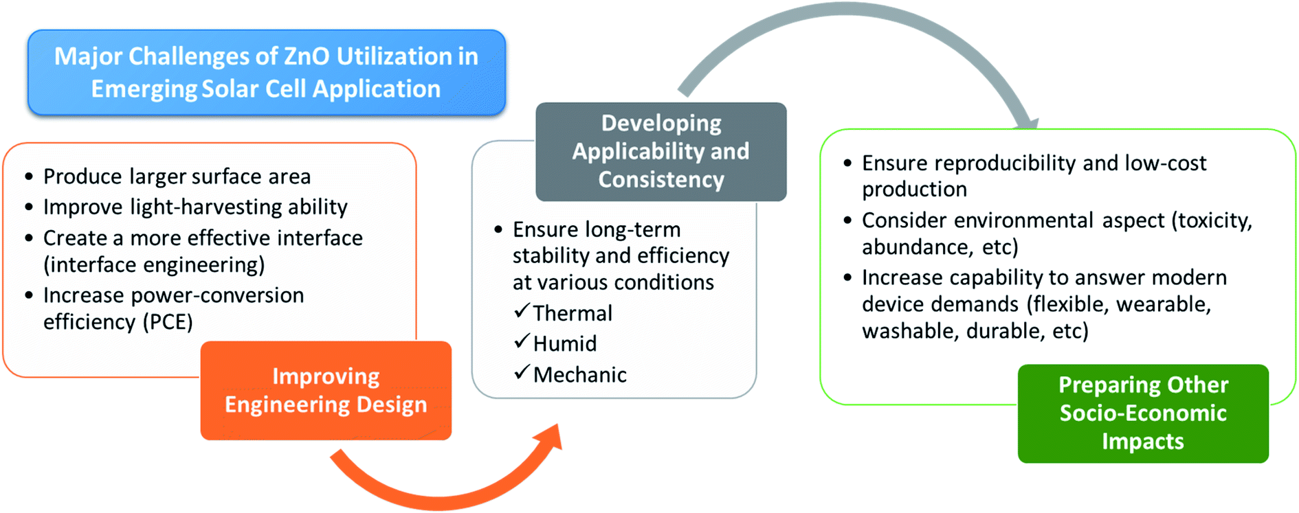 | ||
| Fig. 3 Major challenges for ZnO solar cell development. | ||
In general, emerging solar cell technologies are considered to have low penetration into the market. Thus, progress in achieving a low-cost technique to prepare ZnO with good reproducibility alongside a green method that provides sustainability and environmental-friendliness will boost the positive impacts on the socio-economic aspects. Besides, the capability of the whole device to be easily adjusted for various device requirements (flexible, wearable, durable, washable, etc.) is also vital for enhancing the commercialization.
Conflicts of interest
There are no conflicts to declare.Acknowledgements
L. J. D. and M. I. A. would like to acknowledge the support from Universitas Prasetiya Mulya and the Indonesian Ministry of Research, Technology and Higher Education through INSINAS RISET PRATAMA (No. 47/INS-1/PPK/E4/2018 and No. 35/INS-1/PPK/E4/2019) funding schemes. A. W. would like to acknowledge the funding provided by Institut Teknologi Bandung through ITB Research Fund, Research Group B 2020 (PN-6-01-2020).Notes and references
- R. Senger and K. Bajaj, Phys. Rev. B: Condens. Matter, 2003, 68, 045313 CrossRef.
- G. Oskam, Z. Hu, R. L. Penn, N. Pesika and P. C. Searson, Phys. Rev. E, 2002, 66, 011403 CrossRef.
- D. C. Look, D. C. Reynolds, J. Sizelove, R. Jones, C. W. Litton, G. Cantwell and W. Harsch, Solid State Commun., 1998, 105, 399–401 CrossRef CAS.
- J. Albrecht, P. Ruden, S. Limpijumnong, W. Lambrecht and K. Brennan, J. Appl. Phys., 1999, 86, 6864–6867 CrossRef CAS.
- W. I. Park, J. S. Kim, G.-C. Yi, M. Bae and H.-J. Lee, Appl. Phys. Lett., 2004, 85, 5052–5054 CrossRef CAS.
- H. Tang, K. Prasad, R. Sanjines, P. Schmid and F. Levy, J. Appl. Phys., 1994, 75, 2042–2047 CrossRef CAS.
- V. Noack, H. Weller and A. Eychmüller, J. Phys. Chem. B, 2002, 106, 8514–8523 CrossRef CAS.
- J.-J. Wu, G.-R. Chen, C.-C. Lu, W.-T. Wu and J.-S. Chen, Nanotechnology, 2008, 19, 105702 CrossRef.
- M. Grätzel, Nature, 2001, 414, 338–344 CrossRef.
- A. J. Nozik, Phys. E, 2002, 14, 115–120 CrossRef CAS.
- R. D. Schaller and V. I. Klimov, Phys. Rev. Lett., 2004, 92, 186601 CrossRef CAS.
- I. Robel, V. Subramanian, M. Kuno and P. V. Kamat, J. Am. Chem. Soc., 2006, 128, 2385–2393 CrossRef CAS.
- R. Plass, S. Pelet, J. Krueger, M. Grätzel and U. Bach, J. Phys. Chem. B, 2002, 106, 7578–7580 CrossRef CAS.
- O. Niitsoo, S. K. Sarkar, C. Pejoux, S. Rühle, D. Cahen and G. Hodes, J. Photochem. Photobiol., A, 2006, 181, 306–313 CrossRef CAS.
- L. J. Diguna, Q. Shen, J. Kobayashi and T. Toyoda, Appl. Phys. Lett., 2007, 91, 023116 CrossRef.
- L. J. Diguna, M. Murakami, A. Sato, Y. Kumagai, T. Ishihara, N. Kobayashi, Q. Shen and T. Toyoda, Jpn. J. Appl. Phys., 2006, 45, 5563 CrossRef CAS.
- M. Matsumura, S. Matsudaira, H. Tsubomura, M. Takata and H. Yanagida, Ind. Eng. Chem. Prod. Res. Dev., 1980, 19, 415–421 CrossRef CAS.
- H. Rensmo, K. Keis, H. Lindström, S. Södergren, A. Solbrand, A. Hagfeldt, S.-E. Lindquist, L. Wang and M. Muhammed, J. Phys. Chem. B, 1997, 101, 2598–2601 CrossRef CAS.
- K. Hara, T. Horiguchi, T. Kinoshita, K. Sayama, H. Sugihara and H. Arakawa, Sol. Energy Mater. Sol. Cells, 2000, 64, 115–134 CrossRef CAS.
- H. Horiuchi, R. Katoh, K. Hara, M. Yanagida, S. Murata, H. Arakawa and M. Tachiya, J. Phys. Chem. B, 2003, 107, 2570–2574 CrossRef CAS.
- K. Keis, J. Lindgren, S.-E. Lindquist and A. Hagfeldt, Langmuir, 2000, 16, 4688–4694 CrossRef CAS.
- G. A. Parks, Chem. Rev., 1965, 65, 177–198 CrossRef CAS.
- K. Keis, E. Magnusson, H. Lindström, S.-E. Lindquist and A. Hagfeldt, Sol. Energy Mater. Sol. Cells, 2002, 73, 51–58 CrossRef.
- K. Keis, C. Bauer, G. Boschloo, A. Hagfeldt, K. Westermark, H. Rensmo and H. Siegbahn, J. Photochem. Photobiol., A, 2002, 148, 57–64 CrossRef CAS.
- K. Keis, L. Vayssieres, H. Rensmo, S.-E. Lindquist and A. Hagfeldt, J. Electrochem. Soc., 2001, 148, A149 CrossRef CAS.
- M. Law, L. E. Greene, J. C. Johnson, R. Saykally and P. Yang, Nat. Mater., 2005, 4, 455–459 CrossRef CAS.
- M. Law, L. E. Greene, A. Radenovic, T. Kuykendall, J. Liphardt and P. Yang, J. Phys. Chem. B, 2006, 110, 22652–22663 CrossRef CAS.
- Q. Zhao, T. Xie, L. Peng, Y. Lin, P. Wang, L. Peng and D. Wang, J. Phys. Chem. C, 2007, 111, 17136–17145 CrossRef CAS.
- Y. Hsu, Y. Xi, A. Djurišić and W. Chan, Appl. Phys. Lett., 2008, 92, 133507 CrossRef.
- Z. Chen, Y. Tang, C. Liu, Y. Leung, G. Yuan, L. Chen, Y. Wang, I. Bello, J. Zapien and W. Zhang, J. Phys. Chem. C, 2009, 113, 13433–13437 CrossRef CAS.
- S. Yun, J. Lee, J. Chung and S. Lim, J. Phys. Chem. Solids, 2010, 71, 1724–1731 CrossRef CAS.
- J. Han, F. Fan, C. Xu, S. Lin, M. Wei, X. Duan and Z. L. Wang, Nanotechnology, 2010, 21, 405203 CrossRef.
- A. B. Martinson, J. W. Elam, J. T. Hupp and M. J. Pellin, Nano Lett., 2007, 7, 2183–2187 CrossRef CAS.
- R. Vittal and K.-C. Ho, Renewable Sustainable Energy Rev., 2017, 70, 920–935 CrossRef CAS.
- D. Pourjafari and G. Oskam, in Nanomaterials for Solar Cell Applications, Elsevier, 2019, pp. 145–204 Search PubMed.
- Y.-K. Syu, Y. Tingare, C.-Y. Yeh, J.-S. Yang and J.-J. Wu, RSC Adv., 2016, 6, 59273–59279 RSC.
- K. Funabiki, H. Mase, A. Hibino, N. Tanaka, N. Mizuhata, Y. Sakuragi, A. Nakashima, T. Yoshida, Y. Kubota and M. Matsui, Energy Environ. Sci., 2011, 4, 2186–2192 RSC.
- P. K. Baviskar, D. P. Dubal, S. Majumder, A. Ennaoui and B. R. Sankapal, J. Photochem. Photobiol., A, 2016, 318, 135–141 CrossRef CAS.
- D. Barpuzary, A. S. Patra, J. V. Vaghasiya, B. G. Solanki, S. S. Soni and M. Qureshi, ACS Appl. Mater. Interfaces, 2014, 6, 12629–12639 CrossRef CAS.
- I. Karki, J. Nakarmi, P. Mandal and S. Chatterjee, Appl. Sol. Energy, 2013, 49, 40–45 CrossRef.
- C.-P. Lee, C.-T. Li, M.-S. Fan, S.-R. Li, Y.-J. Huang, L.-Y. Chang, C.-M. Tseng, S.-S. Sun, J.-J. Lin and K.-C. Ho, Electrochim. Acta, 2016, 210, 483–491 CrossRef CAS.
- G.-J. Chang, S.-Y. Lin and J.-J. Wu, Nanoscale, 2014, 6, 1329–1334 RSC.
- S.-Y. Lin and J.-J. Wu, Electrochim. Acta, 2015, 152, 61–67 CrossRef CAS.
- G. S. Selopal, H.-P. Wu, J. Lu, Y.-C. Chang, M. Wang, A. Vomiero, I. Concina and E. W.-G. Diau, Sci. Rep., 2016, 6, 18756 CrossRef CAS.
- J. X. Zhao, Y. Z. Zheng, X. H. Lu, J. F. Chen, X. Tao and W. Zhou, ChemPhysChem, 2013, 14, 1977–1984 CrossRef CAS.
- K. Mahmood and S. B. Park, J. Mater. Chem. A, 2013, 1, 4826–4835 RSC.
- M. Lanjewar and J. V. Gohel, Inorg. Nano-Met. Chem., 2017, 47, 1090–1096 CrossRef CAS.
- S. Aksoy, O. Polat, K. Gorgun, Y. Caglar and M. Caglar, Phys. E, 2020, 121, 114127 CrossRef CAS.
- S. Goel, N. Sinha, H. Yadav, A. J. Joseph and B. Kumar, Phys. E, 2017, 91, 72–81 CrossRef CAS.
- A. K. Rajan and L. Cindrella, Superlattices Microstruct., 2019, 128, 14–22 CrossRef CAS.
- R. K. Chava and M. Kang, J. Alloys Compd., 2017, 692, 67–76 CrossRef CAS.
- A. Saboor, S. M. Shah and H. Hussain, Mater. Sci. Semicond. Process., 2019, 93, 215–225 CrossRef CAS.
- R. Chauhan, M. Shinde, A. Kumar, S. Gosavi and D. P. Amalnerkar, Microporous Mesoporous Mater., 2016, 226, 201–208 CrossRef CAS.
- T. Marimuthu, N. Anandhan and R. Thangamuthu, Appl. Surf. Sci., 2018, 428, 385–394 CrossRef CAS.
- C.-P. Lee, C.-Y. Chou, C.-Y. Chen, M.-H. Yeh, L.-Y. Lin, R. Vittal, C.-G. Wu and K.-C. Ho, J. Power Sources, 2014, 246, 1–9 CrossRef CAS.
- Q. Shen, J. Kobayashi, L. J. Diguna and T. Toyoda, J. Appl. Phys., 2008, 103, 084304 CrossRef.
- P. Yu, K. Zhu, A. G. Norman, S. Ferrere, A. J. Frank and A. J. Nozik, J. Phys. Chem. B, 2006, 110, 25451–25454 CrossRef CAS.
- S. Giménez, I. Mora-Seró, L. Macor, N. Guijarro, T. Lana-Villarreal, R. Gómez, L. J. Diguna, Q. Shen, T. Toyoda and J. Bisquert, Nanotechnology, 2009, 20, 295204 CrossRef.
- G. Zhu, T. Lv, L. Pan, Z. Sun and C. Sun, J. Alloys Compd., 2011, 509, 362–365 CrossRef CAS.
- K. S. Leschkies, R. Divakar, J. Basu, E. Enache-Pommer, J. E. Boercker, C. B. Carter, U. R. Kortshagen, D. J. Norris and E. S. Aydil, Nano Lett., 2007, 7, 1793–1798 CrossRef CAS.
- Y. Choi, M. Seol, W. Kim and K. Yong, J. Phys. Chem. C, 2014, 118, 5664–5670 CrossRef CAS.
- T. Majumder, S. Dhar, P. Chakraborty, K. Debnath and S. P. Mondal, J. Electroanal. Chem., 2018, 813, 92–101 CrossRef CAS.
- L. Luo, G. Lv, B. Li, X. Hu, L. Jin, J. Wang and Y. Tang, Thin Solid Films, 2010, 518, 5146–5152 CrossRef CAS.
- L. J. Diguna, Q. Shen, A. Sato, K. Katayama, T. Sawada and T. Toyoda, Mater. Sci. Eng. C, 2007, 27, 1514–1520 CrossRef CAS.
- J. Luo, Y. X. Wang, J. Sun, Z. S. Yang and Q. F. Zhang, Sol. Energy Mater. Sol. Cells, 2018, 187, 199–206 CrossRef CAS.
- L. Yu and Z. Li, Nanomaterials, 2019, 9, 132 CrossRef CAS.
- Z. Li, L. Yu, H. Wang, H. Yang and H. Ma, Nanomaterials, 2020, 10, 631 CrossRef CAS.
- K. Žídek, M. Abdellah, K. Zheng and T. Pullerits, Sci. Rep., 2014, 4, 1–8 Search PubMed.
- O. E. Semonin, J. M. Luther, S. Choi, H.-Y. Chen, J. Gao, A. J. Nozik and M. C. Beard, Science, 2011, 334, 1530–1533 CrossRef CAS.
- V. Chakrapani, D. Baker and P. V. Kamat, J. Am. Chem. Soc., 2011, 133, 9607–9615 CrossRef CAS.
- J. Duan, Q. Tang, Y. Sun, B. He and H. Chen, RSC Adv., 2014, 4, 60478–60483 RSC.
- M. Eskandari, R. Ghahary, M. Shokri and V. Ahmadi, RSC Adv., 2016, 6, 51894–51899 RSC.
- C. V. Gopi, M. Venkata-Haritha, Y.-S. Lee and H.-J. Kim, J. Mater. Chem. A, 2016, 4, 8161–8171 RSC.
- S. Yun, Y. Qin, A. R. Uhl, N. Vlachopoulos, M. Yin, D. Li, X. Han and A. Hagfeldt, Energy Environ. Sci., 2018, 11, 476–526 RSC.
- N. G. Park, Adv. Energy Mater., 2020, 10, 1903106 CrossRef CAS.
- N. A. N. Ouedraogo, Y. Chen, Y. Y. Xiao, Q. Meng, C. B. Han, H. Yan and Y. Zhang, Nano Energy, 2020, 67, 104249 CrossRef CAS.
- J. A. Schwenzer, L. Rakocevic, T. Abzieher, D. Rueda-Delgado, S. Moghadamzadeh, S. Gharibzadeh, I. M. Hossain, R. Gehlhaar, B. S. Richards and U. Lemmer, IEEE Journal of Photovoltaics, 2020, 10, 777–784 Search PubMed.
- A. Kojima, K. Teshima, Y. Shirai and T. Miyasaka, J. Am. Chem. Soc., 2009, 131, 6050–6051 CrossRef CAS.
- J. Zhao, X. Zheng, Y. Deng, T. Li, Y. Shao, A. Gruverman, J. Shield and J. Huang, Energy Environ. Sci., 2016, 9, 3650–3656 RSC.
- T. Pauportè, in The Future of Semiconductor Oxides in Next-Generation Solar Cells, Elsevier, 2018, pp. 3–43 Search PubMed.
- J. Luo, Y. Wang and Q. Zhang, Sol. Energy, 2018, 163, 289–306 CrossRef CAS.
- G. Yang, H. Tao, P. Qin, W. Ke and G. Fang, J. Mater. Chem. A, 2016, 4, 3970–3990 RSC.
- D. Liu and T. L. Kelly, Nat. Photonics, 2014, 8, 133–138 CrossRef CAS.
- X. Yang, R. Wang, C. Fan, G. Li, Z. Xiong and G. E. Jabbour, Org. Electron., 2014, 15, 2387–2394 CrossRef CAS.
- L. Zuo, Z. Gu, T. Ye, W. Fu, G. Wu, H. Li and H. Chen, J. Am. Chem. Soc., 2015, 137, 2674–2679 CrossRef CAS.
- E. Zheng, Y. Wang, J. Song, X.-F. Wang, W. Tian, G. Chen and T. Miyasaka, J. Energy Chem., 2018, 27, 1461–1467 CrossRef.
- J. Duan, Q. Xiong, H. Wang, J. Zhang and J. Hu, J. Mater. Sci.: Mater. Electron., 2017, 28, 60–66 CrossRef CAS.
- K. Mahmood, B. S. Swain and A. Amassian, Adv. Energy Mater., 2015, 5, 1500568 CrossRef.
- S. Li, P. Zhang, H. Chen, Y. Wang, D. Liu, J. Wu, H. Sarvari and Z. D. Chen, J. Power Sources, 2017, 342, 990–997 CrossRef CAS.
- S. Zhuiykov, in Nanostructured semiconductor oxides for the next generation of electronics and functional devices: properties and applications, Woodhead Publishing, 2014 Search PubMed.
- D. P. Norton, Y. Heo, M. Ivill, K. Ip, S. Pearton, M. F. Chisholm and T. Steiner, Mater. Today, 2004, 7, 34–40 CrossRef CAS.
- Y.-Z. Zheng, E.-F. Zhao, F.-L. Meng, X.-S. Lai, X.-M. Dong, J.-J. Wu and X. Tao, J. Mater. Chem. A, 2017, 5, 12416–12425 RSC.
- K. Mahmood and S. B. Park, Electron. Mater. Lett., 2013, 9, 161–170 CrossRef CAS.
- Y. Chen, Y. Hu, Q. Meng, H. Yan, W. Shuai and Z. Zhang, J. Mater. Sci.: Mater. Electron., 2019, 30, 4726–4736 CrossRef CAS.
- J. Dong, J. Shi, D. Li, Y. Luo and Q. Meng, Appl. Phys. Lett., 2015, 107, 073507 CrossRef.
- J. Dong, Y. Zhao, J. Shi, H. Wei, J. Xiao, X. Xu, J. Luo, J. Xu, D. Li and Y. Luo, ChemComm, 2014, 50, 13381–13384 RSC.
- N. Shibayama, H. Kanda, S.-i. Yusa, S. Fukumoto, A. K. Baranwal, H. Segawa, T. Miyasaka and S. Ito, Nano Convergence, 2017, 4, 1–5 CrossRef.
- M. Dehghan and A. Behjat, RSC Adv., 2019, 9, 20917–20924 RSC.
- Y. Xu, T. Liu, Z. Li, B. Feng, S. Li, J. Duan, C. Ye, J. Zhang and H. Wang, Appl. Surf. Sci., 2016, 388, 89–96 CrossRef CAS.
- S. Li, P. Zhang, Y. Wang, H. Sarvari, D. Liu, J. Wu, Y. Yang, Z. Wang and Z. D. Chen, Nano Res., 2017, 10, 1092–1103 CrossRef CAS.
- X. Dong, H. Hu, B. Lin, J. Ding and N. Yuan, ChemComm, 2014, 50, 14405–14408 RSC.
- L. Kazmerski, F. White and G. Morgan, Appl. Phys. Lett., 1976, 29, 268–270 CrossRef CAS.
- M. Zhong, L. Chai and Y. Wang, Appl. Surf. Sci., 2019, 464, 301–310 CrossRef CAS.
- C. K. Miskin, S. D. Deshmukh, V. Vasiraju, K. Bock, G. Mittal, A. Dubois-Camacho, S. Vaddiraju and R. Agrawal, ACS Appl. Nano Mater., 2019, 2, 1242–1252 CrossRef CAS.
- K. S. Leschkies, T. J. Beatty, M. S. Kang, D. J. Norris and E. S. Aydil, ACS Nano, 2009, 3, 3638–3648 CrossRef CAS.
- J. M. Luther, J. Gao, M. T. Lloyd, O. E. Semonin, M. C. Beard and A. J. Nozik, Adv. Mater., 2010, 22, 3704–3707 CrossRef CAS.
- N. M. Rosas-Laverde, A. Pruna, J. Cembrero, J. Orozco-Messana and F. J. Manjón, Bol. Soc. Esp. Ceram. Vidrio, 2019, 58, 263–273 CrossRef.
- R. Gayen and T. Chakrabarti, Mater. Sci. Semicond. Process., 2019, 100, 1–7 CrossRef CAS.
- S. Qiao, J. Liu, G. Fu, K. Ren, Z. Li, S. Wang and C. Pan, Nano Energy, 2018, 49, 508–514 CrossRef CAS.
- Z. Zang, Appl. Phys. Lett., 2018, 112, 042106 CrossRef.
- T. Minami, T. Miyata and Y. Nishi, Thin Solid Films, 2014, 559, 105–111 CrossRef CAS.
- T. Minami, Y. Nishi and T. Miyata, Appl. Phys. Express, 2013, 6, 044101 CrossRef.
- U. Ozgur, D. Hofstetter and H. Morkoc, Proceedings of the IEEE, 2010, 98, 1255–1268 CAS.
- D.-C. Perng, M.-H. Hong, K.-H. Chen and K.-H. Chen, J. Alloys Compd., 2017, 695, 549–554 CrossRef CAS.
- J. Jean, S. Chang, P. R. Brown, J. J. Cheng, P. H. Rekemeyer, M. G. Bawendi, S. Gradečak and V. Bulović, Adv. Mater., 2013, 25, 2790–2796 CrossRef CAS.
- H. Wang, T. Kubo, J. Nakazaki and H. Segawa, ACS Energy Lett., 2017, 2, 2110–2117 CrossRef CAS.
- A. Tamang, M. Pathirane, R. Parsons, M. M. Schwarz, B. Iheanacho, V. Jovanov, V. Wagner, W. S. Wong and D. Knipp, Opt. Express, 2014, 22, A622–A632 CrossRef CAS.
- B. Wang, X. Zhu, S. Li, M. Chen, N. Liu, H. Yang, M. Ran, H. Lu and Y. Yang, Nanomaterials, 2019, 9, 1263 CrossRef CAS.
- L. Zhu, L. Wang, F. Xue, L. Chen, J. Fu, X. Feng, T. Li and Z. L. Wang, Adv. Sci., 2017, 4, 1600185 CrossRef.
- M. A. Akram, S. Javed, M. Islam, M. Mujahid and A. Safdar, Sol. Energy Mater. Sol. Cells, 2016, 146, 121–128 CrossRef.
- E. Peksu and H. Karaagac, J. Nanomater., 2015, 2015, 516012 Search PubMed.
- K. Yamada, N. Hoshino and T. Nakada, Sci. Technol. Adv. Mater., 2006, 7, 42 CrossRef CAS.
- F.-I. Lai, J.-F. Yang, W.-X. Liao and S.-Y. Kuo, Sci. Rep., 2017, 7, 1–9 CrossRef CAS.
- X. Pu, J. Liu, J. Liang, Y. Xia, W. Feng, Y. Wang and X. Yu, RSC Adv., 2014, 4, 23149–23154 RSC.
- L. Wang, D.-B. Li, K. Li, C. Chen, H.-X. Deng, L. Gao, Y. Zhao, F. Jiang, L. Li and F. Huang, Nat. Energy, 2017, 2, 1–9 Search PubMed.
- J. Yang, J. Lee, J. Lee and W. Yi, J. Power Sources, 2019, 421, 124–131 CrossRef CAS.
- D. Said, A. Ali, M. Khayyat, M. Boustimi, M. Loulou and R. Seoudi, Heliyon, 2019, 5, e02675 CrossRef CAS.
- T. Kawawaki, H. Wang, T. Kubo, K. Saito, J. Nakazaki, H. Segawa and T. Tatsuma, ACS Nano, 2015, 9, 4165–4172 CrossRef CAS.
- F. Yang, Y. Xu, M. Gu, S. Zhou, Y. Wang, K. Lu, Z. Liu, X. Ling, Z. Zhu and J. Chen, J. Mater. Chem. A, 2018, 6, 17688–17697 RSC.
- K. Li, R. Kondrotas, C. Chen, S. Lu, X. Wen, D. Li, J. Luo, Y. Zhao and J. Tang, Sol. Energy, 2018, 167, 10–17 CrossRef CAS.
- A. Kaphle, E. Echeverria, D. N. Mcllroy and P. Hari, RSC Adv., 2020, 10, 7839–7854 RSC.
- Y.-K. Hsu, H.-H. Lin, J.-R. Wu, M.-H. Chen, Y.-C. Chen and Y.-G. Lin, RSC Adv., 2014, 4, 7655–7659 RSC.
- S. Zang, Y. Wang, M. Li, W. Su, H. Zhu, X. Zhang and Y. Liu, Sol. Energy Mater. Sol. Cells, 2017, 169, 264–269 CrossRef CAS.
- C.-H. M. Chuang, P. R. Brown, V. Bulović and M. G. Bawendi, Nat. Mater., 2014, 13, 796–801 CrossRef CAS.
- S. Paulo, E. Palomares and E. Martinez-Ferrero, Nanomaterials, 2016, 6, 157 CrossRef.
- H. Y. Abbasi, A. Habib and M. Tanveer, J. Alloys Compd., 2017, 690, 21–26 CrossRef CAS.
- V. González, I. López, R. M. Palma, Y. Peña and I. Gómez, Mater. Res. Express, 2020, 7, 075005 CrossRef.
- M. A. Halim, Nanomaterials, 2013, 3, 22–47 CrossRef CAS.
- J. Huang, Z. Yin and Q. Zheng, Energy Environ. Sci., 2011, 4, 3861–3877 RSC.
- W. J. Beek, M. M. Wienk and R. A. Janssen, Adv. Mater., 2004, 16, 1009–1013 CrossRef CAS.
- Y. Hames, Z. Alpaslan, A. Kösemen, S. E. San and Y. Yerli, Sol. Energy, 2010, 84, 426–431 CrossRef CAS.
- J. Liu, S. Wang, Z. Bian, M. Shan and C. Huang, Appl. Phys. Lett., 2009, 94, 173107 CrossRef.
- S. Dayal, N. Kopidakis, D. C. Olson, D. S. Ginley and G. Rumbles, Nano Lett., 2010, 10, 239–242 CrossRef CAS.
- J. Qi, J. Chen, W. Meng, X. Wu, C. Liu, W. Yue and M. Wang, Synth. Met., 2016, 222, 42–65 CrossRef CAS.
- W. J. Beek, M. M. Wienk and R. A. Janssen, Adv. Funct. Mater., 2006, 16, 1112–1116 CrossRef CAS.
- L. J. A. Koster, W. J. van Strien, W. J. Beek and P. W. Blom, Adv. Funct. Mater., 2007, 17, 1297–1302 CrossRef CAS.
- S. D. Oosterhout, M. M. Wienk, S. S. Van Bavel, R. Thiedmann, L. J. A. Koster, J. Gilot, J. Loos, V. Schmidt and R. A. Janssen, Nat. Mater., 2009, 8, 818–824 CrossRef CAS.
- S.-S. Li and C.-W. Chen, J. Mater. Chem. A, 2013, 1, 10574–10591 RSC.
- W. J. Beek, L. H. Slooff, M. M. Wienk, J. M. Kroon and R. A. Janssen, Adv. Funct. Mater., 2005, 15, 1703–1707 CrossRef CAS.
- W. J. Beek, M. M. Wienk, M. Kemerink, X. Yang and R. A. Janssen, J. Phys. Chem. B, 2005, 109, 9505–9516 CrossRef CAS.
- D. J. Moet, L. J. A. Koster, B. de Boer and P. W. Blom, Chem. Mater., 2007, 19, 5856–5861 CrossRef CAS.
- A. Thomas, R. Vinayakan and V. Ison, RSC Adv., 2020, 10, 16693–16699 RSC.
- P. Ravirajan, A. M. Peiró, M. K. Nazeeruddin, M. Graetzel, D. D. Bradley, J. R. Durrant and J. Nelson, J. Phys. Chem. B, 2006, 110, 7635–7639 CrossRef CAS.
- I. Gonzalez-Valls and M. Lira-Cantu, Energy Environ. Sci., 2009, 2, 19–34 RSC.
- S. Jung, J. Lee, J. Seo, U. Kim, Y. Choi and H. Park, Nano Lett., 2018, 18, 1337–1343 CrossRef CAS.
- J. Pei, K. Feng, X. Zhao, Y. Hao, Y. Wei, B. Sun, Y. Li, S. Chen and H. Lv, Opt. Commun., 2018, 427, 294–300 CrossRef CAS.
- A. Galdámez-Martinez, G. Santana, F. Güell, P. R. Martínez-Alanis and A. Dutt, Nanomaterials, 2020, 10, 857 CrossRef.
- D. C. Olson, J. Piris, R. T. Collins, S. E. Shaheen and D. S. Ginley, Thin Solid Films, 2006, 496, 26–29 CrossRef CAS.
- D. C. Olson, Y.-J. Lee, M. S. White, N. Kopidakis, S. E. Shaheen, D. S. Ginley, J. A. Voigt and J. W. Hsu, J. Phys. Chem. C, 2007, 111, 16640–16645 CrossRef CAS.
- L. Baeten, B. Conings, H. G. Boyen, J. D'Haen, A. Hardy, M. D'Olieslaeger, J. V. Manca and M. K. Van Bael, Adv. Mater., 2011, 23, 2802–2805 CrossRef CAS.
- C. Thu, P. Ehrenreich, K. K. Wong, E. Zimmermann, J. Dorman, W. Wang, A. Fakharuddin, M. Putnik, C. Drivas and A. Koutsoubelitis, Sci. Rep., 2018, 8, 1–8 CrossRef CAS.
- S. B. Dkhil, M. Gaceur, W. Dachraoui, D. Hannani, S. Fall, F. Brunel, M. Wang, G. Poize, J. Mawyin and I. Shupyk, Sol. Energy Mater. Sol. Cells, 2017, 159, 608–616 CrossRef.
- A. Alshanableh, S. T. Tan, C. C. Yap, H. B. Lee, H. F. Oleiwi, K. J. Hong, M. H. H. Jumali and M. Yahaya, Mater. Sci. Eng., B, 2018, 238, 136–141 CrossRef.
- J. Han, Z. Liu, X. Zheng, K. Guo, X. Zhang, T. Hong, B. Wang and J. Liu, RSC Adv., 2014, 4, 23807–23814 RSC.
- D. C. Olson, Y.-J. Lee, M. S. White, N. Kopidakis, S. E. Shaheen, D. S. Ginley, J. A. Voigt and J. W. Hsu, J. Phys. Chem. C, 2008, 112, 9544–9547 CrossRef CAS.
- D. C. Olson, S. E. Shaheen, M. S. White, W. J. Mitchell, M. F. van Hest, R. T. Collins and D. S. Ginley, Adv. Funct. Mater., 2007, 17, 264–269 CrossRef CAS.
- A. Samavati, Z. Samavati, A. Ismail, M. Othman, M. A. Rahman and I. Amiri, RSC Adv., 2018, 8, 1418–1426 RSC.
- M. S. White, D. C. Olson, N. Kopidakis, A. M. Nardes, D. S. Ginley and J. J. Berry, Phys. Status Solidi, 2010, 207, 1257–1265 CrossRef CAS.
- J. Bouclé, H. J. Snaith and N. C. Greenham, J. Phys. Chem. C, 2010, 114, 3664–3674 CrossRef.
- D. C. Olson, S. E. Shaheen, R. T. Collins and D. S. Ginley, J. Phys. Chem. C, 2007, 111, 16670–16678 CrossRef CAS.
- M. Batmunkh, Y. L. Zhong and H. Zhao, Adv. Mater., 2020, 32, 2000631 CrossRef CAS.
- H.-L. Yip and A. K.-Y. Jen, Energy Environ. Sci., 2012, 5, 5994–6011 RSC.
- A. Manor, E. A. Katz, T. Tromholt and F. C. Krebs, Sol. Energy Mater. Sol. Cells, 2012, 98, 491–493 CrossRef CAS.
- Y. Jouane, S. Colis, G. Schmerber, P. Kern, A. Dinia, T. Heiser and Y.-A. Chapuis, J. Mater. Chem., 2011, 21, 1953–1958 RSC.
- T. C. Monson, M. T. Lloyd, D. C. Olson, Y. J. Lee and J. W. Hsu, Adv. Mater., 2008, 20, 4755–4759 CrossRef CAS.
- S. K. Hau, H.-L. Yip, N. S. Baek, J. Zou, K. O'Malley and A. K.-Y. Jen, Appl. Phys. Lett., 2008, 92, 225 CrossRef.
- H. L. Yip, S. K. Hau, N. S. Baek, H. Ma and A. K. Y. Jen, Adv. Mater., 2008, 20, 2376–2382 CrossRef CAS.
- H.-L. Yip, S. K. Hau, N. S. Baek and A. K.-Y. Jen, Appl. Phys. Lett., 2008, 92, 179 Search PubMed.
- H. Cao, W. He, Y. Mao, X. Lin, K. Ishikawa, J. H. Dickerson and W. P. Hess, J. Power Sources, 2014, 264, 168–183 CrossRef CAS.
- Z. Liang, Q. Zhang, L. Jiang and G. Cao, Energy Environ. Sci., 2015, 8, 3442–3476 RSC.
- Y.-J. Cheng, C.-H. Hsieh, Y. He, C.-S. Hsu and Y. Li, J. Am. Chem. Soc., 2010, 132, 17381–17383 CrossRef CAS.
- Y. He, H.-Y. Chen, J. Hou and Y. Li, J. Am. Chem. Soc., 2010, 132, 1377–1382 CrossRef CAS.
- S. Ganesan, S. R. Gollu, A. Kushwaha and D. Gupta, Opt. Mater., 2019, 94, 430–435 CrossRef CAS.
- C. M. Amb, S. Chen, K. R. Graham, J. Subbiah, C. E. Small, F. So and J. R. Reynolds, J. Am. Chem. Soc., 2011, 133, 10062–10065 CrossRef CAS.
- A. Djurišić, A. M. C. Ng and X. Chen, Prog. Quantum Electron., 2010, 34, 191–259 CrossRef.
- K. Takanezawa, K. Hirota, Q.-S. Wei, K. Tajima and K. Hashimoto, J. Phys. Chem. C, 2007, 111, 7218–7223 CrossRef CAS.
- C.-Y. Chou, J.-S. Huang, C.-H. Wu, C.-Y. Lee and C.-F. Lin, Sol. Energy Mater. Sol. Cells, 2009, 93, 1608–1612 CrossRef CAS.
- R. B. Ambade, S. B. Ambade, R. S. Mane and S.-H. Lee, ACS Appl. Mater. Interfaces, 2015, 7, 7951–7960 CrossRef CAS.
- N. Sekine, C.-H. Chou, W. L. Kwan and Y. Yang, Org. Electron., 2009, 10, 1473–1477 CrossRef CAS.
- S. Y. Ryu, J. H. Seo, H. Hafeez, M. Song, J. Y. Shin, D. H. Kim, Y. C. Jung and C. S. Kim, J. Phys. Chem. C, 2017, 121, 9191–9201 CrossRef CAS.
- R. Thitima, C. Patcharee, S. Takashi and Y. Susumu, Solid-State Electron., 2009, 53, 176–180 CrossRef CAS.
- Y. Vaynzof, D. Kabra, L. Zhao, P. K. Ho, A. T.-S. Wee and R. H. Friend, Appl. Phys. Lett., 2010, 97, 156 CrossRef.
- C.-T. Chen, F.-C. Hsu, S.-W. Kuan and Y.-F. Chen, Sol. Energy Mater. Sol. Cells, 2011, 95, 740–744 CrossRef CAS.
- H. Ma, H. L. Yip, F. Huang and A. K. Y. Jen, Adv. Funct. Mater., 2010, 20, 1371–1388 CrossRef CAS.
- C.-H. Hsieh, Y.-J. Cheng, P.-J. Li, C.-H. Chen, M. Dubosc, R.-M. Liang and C.-S. Hsu, J. Am. Chem. Soc., 2010, 132, 4887–4893 CrossRef CAS.
- D. Zheng, W. Huang, P. Fan, Y. Zheng, J. Huang and J. Yu, ACS Appl. Mater. Interfaces, 2017, 9, 4898–4907 CrossRef CAS.
- S. R. Gollu, R. Sharma, G. Srinivas, S. Kundu and D. Gupta, Org. Electron., 2016, 29, 79–87 CrossRef CAS.
- J. Wei, G. Ji, C. Zhang, L. Yan, Q. Luo, C. Wang, Q. Chen, J. Yang, L. Chen and C.-Q. Ma, ACS Nano, 2018, 12, 5518–5529 CrossRef CAS.
- Y. Cao, D. Wu, P. Zhu, D. Shan, X. Zeng and J. Xu, Nanomaterials, 2020, 10, 775 CrossRef CAS.
- F. Bu, W. Shen, X. Zhang, Y. Wang, L. A. Belfiore and J. Tang, Nanomaterials, 2020, 10, 80 CrossRef CAS.
- W. Shen, G. Zhao, X. Zhang, F. Bu, J. Yun and J. Tang, Nanomaterials, 2020, 10, 944 CrossRef CAS.
- K.-S. Shin, K.-H. Lee, H. H. Lee, D. Choi and S.-W. Kim, J. Phys. Chem. C, 2010, 114, 15782–15785 CrossRef CAS.
- A. K. K. Kyaw, X. Sun, S. T. Tan, Y. Divayana and H. V. Demir, IEEE J. Sel. Top. Quantum Electron., 2010, 16, 1700–1706 CAS.
- M. Zafar, B. Kim and D.-H. Kim, Mater. Chem. Phys., 2020, 240, 122076 CrossRef CAS.
- G. Chen, T. Wang, C. Li, L. Yang, T. Xu, W. Zhu, Y. Gao and B. Wei, Org. Electron., 2016, 36, 50–56 CrossRef CAS.
- M. Ramírez-Como, V. Balderrama, A. Sacramento, L. Marsal, G. Lastra and M. Estrada, Sol. Energy, 2019, 181, 386–395 CrossRef.
- M.-S. White, D. Olson, S. Shaheen, N. Kopidakis and D. S. Ginley, Appl. Phys. Lett., 2006, 89, 143517 CrossRef.
- T. Yang, W. Cai, D. Qin, E. Wang, L. Lan, X. Gong, J. Peng and Y. Cao, J. Phys. Chem. C, 2010, 114, 6849–6853 CrossRef CAS.
- W. Zhao, S. Zhang and J. Hou, Sci. China: Chem., 2016, 59, 1574–1582 CrossRef CAS.
- X. Li, X. Liu, W. Zhang, H.-Q. Wang and J. Fang, Chem. Mater., 2017, 29, 4176–4180 CrossRef CAS.
- X. Wen, A. Nowak-Król, O. Nagler, F. Kraus, N. Zhu, N. Zheng, M. Müller, D. Schmidt, Z. Xie and F. Würthner, Angew. Chem., 2019, 131, 13185–13189 CrossRef.
- N. Shrivastava, H. Barbosa, K. Ali and S. K. Sharma, in Solar Cells – From Material to Device Technology, Springer International Publishing, 2020, pp. 55–78 Search PubMed.
| This journal is © The Royal Society of Chemistry 2020 |