
 Open Access Article
 This Open Access Article is licensed under a Creative Commons Attribution-Non Commercial 3.0 Unported Licence
The synthesis of competing phase GeSe and GeSe2 2D layered materials
Kentaro Yumigeta,
Cassondra Brayfield ,
Hui Cai,
Debarati Hajra,
Mark Blei,
Sijie Yang,
Yuxia Shen and
S. Tongay*
,
Hui Cai,
Debarati Hajra,
Mark Blei,
Sijie Yang,
Yuxia Shen and
S. Tongay*
Materials Science and Engineering, School for Engineering of Matter, Transport and Energy, Arizona State University, Tempe, AZ 85287, USA. E-mail: sefaattin.tongay@asu.edu
First published on 16th October 2020
Abstract
We demonstrate the synthesis of layered anisotropic semiconductor GeSe and GeSe2 nanomaterials through low temperature (∼400 °C) and atmospheric pressure chemical vapor deposition using halide based precursors. Results show that GeI2 and H2Se precursors successfully react in the gas-phase and nucleate on a variety of target substrates including sapphire, Ge, GaAs, or HOPG. Layer-by-layer growth takes place after nucleation to form layered anisotropic materials. Detailed SEM, EDS, XRD, and Raman spectroscopy measurements together with systematic CVD studies reveal that the substrate temperature, selenium partial pressure, and the substrate type ultimately dictate the resulting stoichiometry and phase of these materials. Results from this work introduce the phase control of Ge and Se based nanomaterials (GeSe and GeSe2) using halide based CVD precursors at ATM pressures and low temperatures. Overall findings also extend our fundamental understanding of their growth by making the first attempt to correlate growth parameters to resulting competing phases of Ge–Se based materials.
Introduction
Two-dimensional (2D) materials are atomically thin material systems with extraordinary optical, electrical, thermal, and magnetic properties.1,2 Post-transition metal monochalcogenide (PTMCs) materials are members of this large 2D materials family and have the general chemical formula of MX3,4 wherein M stands for metals from groups IIIA and IVA (In, Ga, Ge, Sn) and X is VIA chalcogenides (S, Se, and Te). These material systems have shown unique properties that are vastly different from other 2D systems such as dichalcogenides or trichalcogenides.3,5 Because of small exciton binding energies (∼10–20 meV) and indirect gap from bulk to monolayers, they are potential photovoltaic materials with efficient e–h generation and separation characteristics. They have been proposed as active semiconductors for water splitting applications owing to their favorable band alignment characteristics with respect to reduction and oxidization energies.6 Recently, GeSe, GeTe, SnSe, and their ternary alloys have been shown to be highly efficient new-class of phase change materials and world record ZT values were also reported on SnSe from PTMCs family.7While germanium based van der Waals (vdW) crystals have been synthesized in the past using the modified Bridgman-Stockberger method,8 it was only until recently GeSe and GeS bulk crystals have been commercialized. The synthesis procedures and protocols for bulk GeSe2 vdW crystal – another layered phase in the Ge–Se diagram – is still lacking. Despite their potential, the synthesis of ultrathin GeSe2 is still at its seminal stages and experimental studies rely on exfoliation.9 GeSe2 synthesis by CVD using GeI4 and Se has been reported.10 Recently, Hu et al. have synthesized GeSe by salt-assisted CVD using GeSe2 precursor.11 However, reported GeSe synthesis by CVD is limited and the method to control the phase of Ge–Se system during CVD is unknown. 2D or ultra-thin Ge based layered materials are commercially still not available due to a fundamental knowledge gap in synthesis of these materials.
Here for the first time, we report GeI2 and Se precursor based chemical vapor deposition technique (CVD) for depositing GeSe and GeSe2 ultrathin nanomaterials onto a variety of substrates. Our systematic studies show that the technique relies on the high temperature reaction of H2Se vapor with GeI2 in close proximity to other substrates. When these two precursors react, CVD growth produces either GeSe or GeSe2 depending on the substrate type, target temperature, and Se partial pressure. Both materials crystallize in their layered form and their composition as well as the crystal structures can be controlled by careful thermal profiling depending on the substrate type and overall growth temperature. This process takes place at low temperature (∼400 °C) which is essential to its compatibility with the semiconductor industry. Raman spectroscopy, energy dispersive X-ray spectroscopy (EDS), scanning electron microscopy (SEM), angle resolved Raman spectroscopy (ARS), and our CVD technique establish the first ever growth of GeSe by halide based precursor and the phase control between GeSe and GeSe2.
Chemical vapor deposition of GeSe and GeSe2
The proposed technique relies on the reaction of GeI2 and Se in close proximity to target substrates as shown in Fig. 1. In this process, GeI2 and Se precursors were selected mainly because of their low melting points, high vapor pressures and chemical reactivities. Selenium powder melts at 220 °C and GeI2 sublimes at 240 °C. In order to reach sufficient and similar vapor Se and Ge pressures, we have placed our GeI2 at the center of the 1 inch diameter single zone furnace and kept at ∼500 °C, while Se powder was approximately at 11–15 cm from GeI2 at 410–460 °C. Here, Se precursor temperature was systematically varied by changing the position of the Se powder (Fig. 1a). The temperature profiling (Fig. 1b) shows the locations of Se, GeI2, and substrates and their keep temperatures, respectively. For simplicity, we denote the Se precursor temperature as TSe, the GeI2 precursor temperature as TGeI2 and the substrate temperature as Tg. In a typical growth, we have used 40 mg of Se powder (99.999%, Sigma-Aldrich) and 40 mg of GeI2 powder (99.999%, Alfa Aesar). These powders were placed on two quartz boats and 3 standard cubic centimeters per minute (sccm) of Ar and 7 sccm of H2 were used as carrier gas at atmospheric pressure. In our study, substrates were selected from Ge (100) (University wafer), GaAs (100) (American Xtal Technology), c-cut sapphire (Ckplas), Highly oriented pyrolytic graphite (HOPG) (Materials Quartz).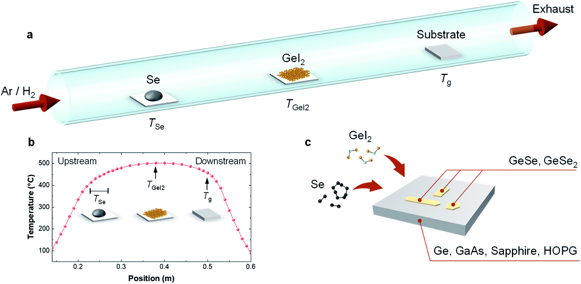 | ||
| Fig. 1 (a) Schematic diagram of the CVD growth of GeSe and GeSe2 ultrathin layers. (b) Temperature profile of the furnace and the position of precursors in relation to the target substrate. (c) Schematic description of GeSe and GeSe2 formation process on various substrates. | ||
Growth and the effect of the substrate
Synthesis was carried out using a variety of different substrates such as germanium, GaAs, sapphire, and graphite vdW surfaces (Fig. 1a and b). Typical growth at Tg = 420 °C using germanium substrates produced rectangular phased GeSe ultra-thin materials which measures tens of microns in lateral sizes. Comparison between Raman spectroscopy data collected from Bridgman grown GeSe crystals and GeSe films show that material crystalizes in alpha-phase GeSe (Fig. 2b). The full width at half maximum (FWHM) of the Raman spectrum from CVD-grown GeSe (4.8 cm−1) is much sharper compared to FWHM of Bridgman grown GeSe crystal (6.3 cm−1) highlighting the crystallinity of the as-grown GeSe sheets. Energy-dispersive X-ray spectroscopy (EDS) measurements on CVD grown GeSe also confirm the stoichiometry of the synthesized layers (Fig. 2c).In order to determine the crystallinity and the degree of anisotropy (measure of crystalline anisotropy of the crystal), we have further performed angle resolved Raman spectroscopy measurements as shown in Fig. 2h. Previously, this method has been used for other 2D anisotropic material systems to provide a fast, quick, noncontact optical method to determine the crystalline orientation.12–17 In this method, Raman intensity of an individual mode is plotted with respect to the laser polarization angle as shown in Fig. 2h. Here, the polarization angle is defined as zero 0° when the laser polarization vector is parallel along the longer edge (large-aspect ratio). B13g mode at 153 cm−1 as well as A1g mode at 190 cm−1 display four-fold symmetry associated with their Raman tensor characteristics, and thus cannot be used to determine the crystal orientation of GeSe. In contrast, A2g mode and A3g show two-fold symmetry which are suitable to determine the crystal orientation using optical techniques. A2g and A3g mode Raman mode intensity maximizes when the polarization vector angle is ∼90° and ∼0°, respectively. Overall 2-lobed features demonstrate that synthesized GeSe sheets are highly crystalline and have good anisotropy. We note however that the full coverage growth is rather challenging since the nucleation density is small and the lateral growth speed is slow.
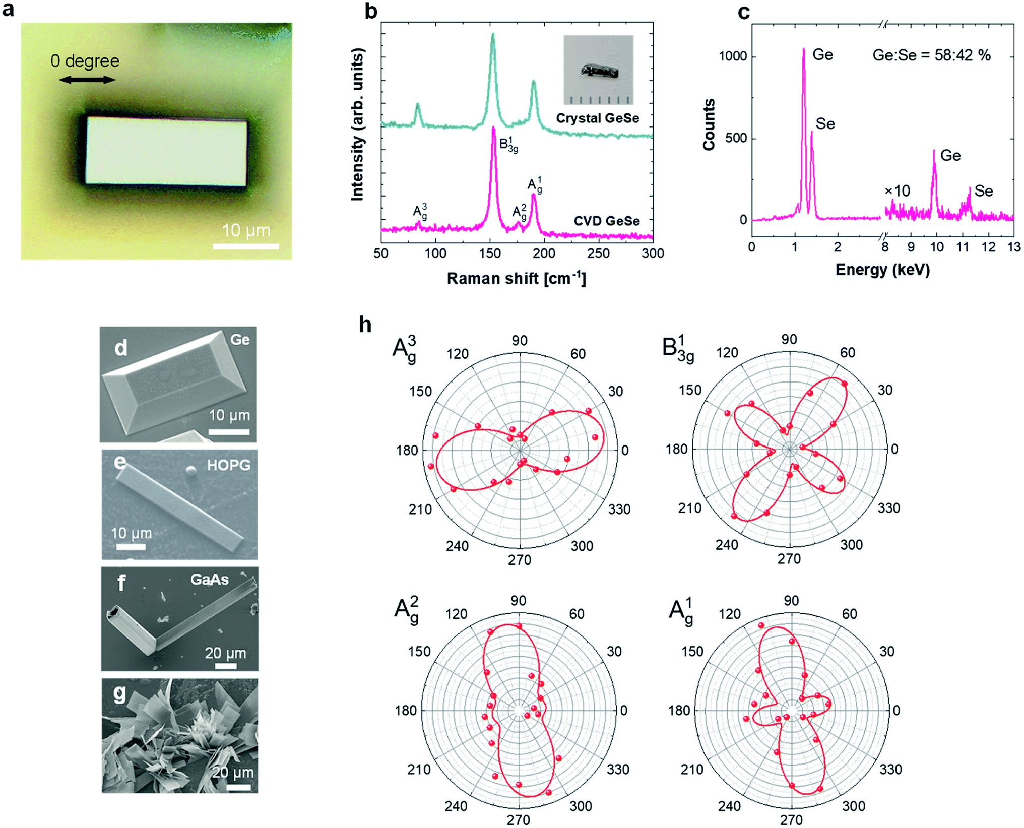 | ||
| Fig. 2 (a) Optical image of CVD-grown GeSe. (b) Comparison between the Raman spectra of bulk GeSe crystal and CVD-grown GeSe. (c) EDS spectrum of CVD-grown GeSe. (d–f). SEM image of GeSe on various substrates. (g) SEM images from flower-like lamellar GeSe sheets. (h) Angle resolved Raman spectra contour plots shown for different Raman modes. | ||
From the optical and SEM images, we find that the surface type and characteristics play a significant role in the type of growth mode. For example, truncated rectangular pyramidal crystals shown in Fig. 2d are attained on single crystal germanium substrates, while flat thin GeSe sheets form on HOPG surfaces (Fig. 2e). On the other hand, the sheets grown on GaAs substrate have out of the plane growth similar to flower like features as shown in Fig. 2f. This might be related to the fact that the elastic energy of GeSe on the substrates is 0.032 meV on Ge(100), 0.046 meV on GaAs. This higher elastic energy on GaAs may promote out-of-plane growth of GeSe.18 In contrast, the elastic energy of HOPG is small since the substrate is a known van der Waals material and may promote layer-by-layer growth. Here, we note that when the flow rate is much higher (Ar at 20 sccm, H2 at 50 sccm), the growth speed increases dramatically and the system deviates from layer-by-layer growth mode resulting in similar flower-like features on other substrates as well (Fig. 2g).
Competition between GeSe and GeSe2 and phase control
In our studies, we have found that the crystal shape on GaAs substrate varies with changing TSe (Fig. 3a). Quasi-1D ribbons grew at TSe = 410 and 430 °C whereas GeSe2 are observed above TSe = 440 °C, however, the shape was elongated hexagonal at 440 °C and ribbon-like at 460 °C. We have confirmed that the stoichiometry of the grown ultrathin sheets are ∼1![[thin space (1/6-em)]](https://www.rsc.org/images/entities/char_2009.gif) :1 for TSe < 430 °C and ∼1:1.6 for TSe > 430 °C by EDS measurement (Fig. 3b). We further confirmed by Raman spectroscopy that the crystals for TSe < 430 °C shows GeSe spectrum while for TSe > 430 °C shows GeSe2 (Fig. 3c) which marks the first synthesis of GeSe2 nanosheets. In the phase diagram of germanium selenide (Fig. 3d), GeSe2 grows at higher temperatures compared to GeSe. Our studies, however, show that GeSe and GeSe2 ultrathin sheets can be grown at the same temperature by simply changing the Se partial pressure (Fig. 3a and e). It is also noteworthy that the temperature ranges show significant differences in our CVD process compared to established bulk phase diagrams19 which can be attributed to the fact that phase diagrams deviate significantly going from bulk to nanomaterials due to differences in surface to volume ratio. Even though GeSe and GeSe2 call for different growth temperatures, our process enables a GeSe to GeSe2 phase transition by increasing the Se concentration without changing the substrate temperature.
:1 for TSe < 430 °C and ∼1:1.6 for TSe > 430 °C by EDS measurement (Fig. 3b). We further confirmed by Raman spectroscopy that the crystals for TSe < 430 °C shows GeSe spectrum while for TSe > 430 °C shows GeSe2 (Fig. 3c) which marks the first synthesis of GeSe2 nanosheets. In the phase diagram of germanium selenide (Fig. 3d), GeSe2 grows at higher temperatures compared to GeSe. Our studies, however, show that GeSe and GeSe2 ultrathin sheets can be grown at the same temperature by simply changing the Se partial pressure (Fig. 3a and e). It is also noteworthy that the temperature ranges show significant differences in our CVD process compared to established bulk phase diagrams19 which can be attributed to the fact that phase diagrams deviate significantly going from bulk to nanomaterials due to differences in surface to volume ratio. Even though GeSe and GeSe2 call for different growth temperatures, our process enables a GeSe to GeSe2 phase transition by increasing the Se concentration without changing the substrate temperature.
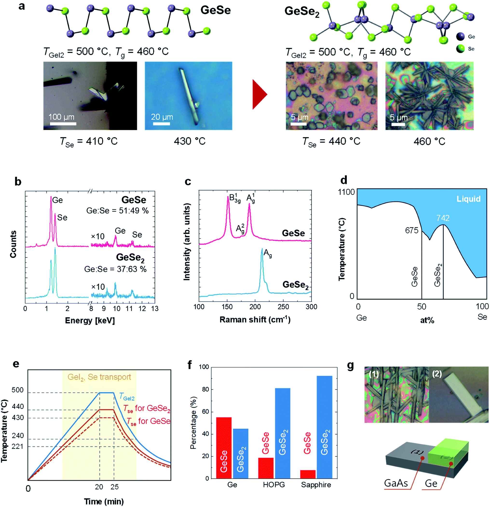 | ||
| Fig. 3 (a) Crystal structures and optical image of grown GeSe and GeSe2. GeSe grows at lower TSe while GeSe2 grows at higher TSe. TGeI2 and Tg are fixed. (b) Raman spectra and (c) EDS spectra of GeSe and GeSe2 on GaAs. (d) Phase diagram of Ge–Se binary system. (e) Temperature profile of CVD growth. (f) Substrate dependence of the percentage of GeSe vs. GeSe2 coverage on different substrates when TGeI2 and Tg are fixed but TSe is varied. (g) Crystals on GaAs (c.1) without and (c.2) with Ge substrate capping. | ||
Raman spectroscopy measurements on the synthesized GeSe2 sheets show that the Raman finger-prints closely match β phase GeSe2 spectra (Fig. 4b)20,21 and the SEM EDS elemental spectra shows that the stoichiometry of these crystals are very close to 1:1.8 (Fig. 4c). To determine the crystallinity and the anisotropy of GeSe2 crystal, we have collected angle resolved Raman spectrum. The Raman intensity of each mode is plotted with respect to the laser polarization angle in Fig. 4d and e. Overall, A1g mode at 211 cm−1, A5g mode at 86 cm−1 and A6g mode at 80 cm−1 shows four-fold symmetry. On the other hand, A2g mode at 118 cm−1, A3g mode at 100 cm−1 and A4g mode at 90 cm−1 shows two-fold symmetry which can be used to determine the crystal orientation. The Raman intensity of A2g mode and A3g mode is strong when the laser polarization is along with the ribbon while A4g becomes minimum. Further study is much needed to understand the polarization response of these prominent Raman modes in GeSe2 nanosheets.
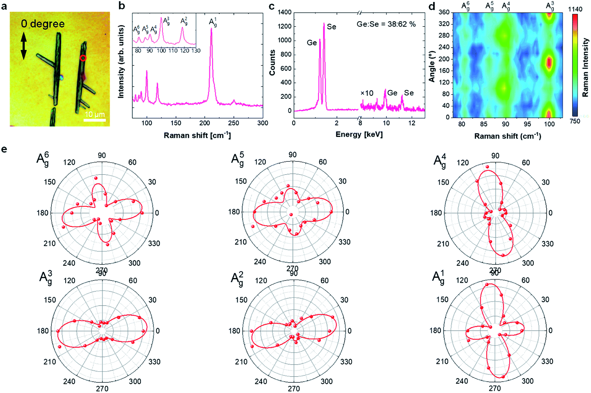 | ||
| Fig. 4 (a) Optical image of GeSe2. (b) Raman spectrum of GeSe2. Inset shows the magnified spectrum of Raman modes. (c) EDS spectrum of GeSe2. (d) Angle resolved Raman spectra and (e) contour plots for fundamental Raman modes (A6g, A5g, A4g, A3g) for GeSe2. | ||
Conclusion
Here, we have reported on a new halide precursor based chemical vapor deposition technique to synthesize GeSe and the method to control two competing phases of GeSe and GeSe2 based nanosheets onto different temperatures. The growth takes place at atmospheric pressure and at room temperature which is attractive for scalability considerations. Interestingly, our process enables us to synthesize both GeSe and GeSe2 by simply adjusting the Se partial pressure without the need to change the substrate temperature which is generally needed for other material systems with different temperature growth windows. Established low temperature and atmospheric pressure growth process extends the fundamental knowledge of bottom-up growth for vdW layered material systems.Conflicts of interest
There are no conflicts of interest declared.Acknowledgements
S. T. acknowledges funding from DOE-SC0020653, Army Research Office W911NF-18-1-0381, NSF CMMI 1933214, and NSF DMR 1552220, 1955889, and 1726213. We acknowledge the use of facilities within the Eyring Materials Center at Arizona State University supported in part by NNCI-ECCS-1542160.References
- Q. H. Wang, K. Kalantar-Zadeh, A. Kis, J. N. Coleman and M. S. Strano, Electronics and optoelectronics of two-dimensional transition metal dichalcogenides, Nat. Nanotechnol., 2012, 7(11), 699–712 CrossRef CAS.
- M. Tran, K. Kline, Y. Qin, Y. Shen, M. D. Green and S. Tongay, 2D coordination polymers: design guidelines and materials perspective, Appl. Phys. Rev., 2019, 6(4), 041311 Search PubMed.
- L. Xu, M. Yang, S. J. Wang and Y. P. Feng, Electronic and optical properties of the monolayer group-IV monochalcogenides MX (M = Ge, Sn; X = S, Se, Te), Phys. Rev. B, 2017, 95(23), 235434 CrossRef.
- H. Cai, B. Chen, M. Blei, S. L. Y. Chang, K. Wu, H. Zhuang and S. Tongay, Abnormal band bowing effects in phase instability crossover region of GaSe1-xTe x nanomaterials, Nat. Commun., 2018, 9(1), 1927 CrossRef.
- D. T. Do, S. D. Mahanti and C. W. Lai, Spin splitting in 2D monochalcogenide semiconductors, Sci. Rep., 2015, 5, 17044 CrossRef CAS.
- H. L. Zhuang and R. G. Hennig, Single-Layer Group-III Monochalcogenide Photocatalysts for Water Splitting, Chem. Mater., 2013, 25(15), 3232–3238 CrossRef CAS.
- C. Chang, M. H. Wu, D. S. He, Y. L. Pei, C. F. Wu, X. F. Wu, H. L. Yu, F. Y. Zhu, K. D. Wang, Y. Chen, L. Huang, J. F. Li, J. Q. He and L. D. Zhao, 3D charge and 2D phonon transports leading to high out-of-plane ZT in n-type SnSe crystals, Science, 2018, 360(6390), 778–782 CrossRef CAS.
- V. L. Cardetta, A. M. Mancini and A. Rizzo, Melt growth of single crystal ingots of GaSe by Bridgman-Stockbarger's method, J. Cryst. Growth, 1972, 16(2), 183–185 CrossRef CAS.
- Y. Yang, S.-C. Liu, W. Yang, Z. Li, Y. Wang, X. Wang, S. Zhang, Y. Zhang, M. Long, G. Zhang, D.-J. Xue, J.-S. Hu and L.-J. Wan, Air-Stable In-Plane Anisotropic GeSe2 for Highly Polarization-Sensitive Photodetection in Short Wave Region, J. Am. Chem. Soc., 2018, 140(11), 4150–4156 CrossRef CAS.
- X. Zhou, X. Hu, S. Zhou, Q. Zhang, H. Li and T. Zhai, Ultrathin 2D GeSe2 Rhombic Flakes with High Anisotropy Realized by van der Waals Epitaxy, Adv. Funct. Mater., 2017, 27, 1703858 CrossRef.
- X. Hu, P. Huang, K. Liu, B. Jin, X. Zhang, X. Zhang, X. Zhou and T. Zhai, Salt-Assisted Growth of Ultrathin GeSe Rectangular Flakes for Phototransistors with Ultrahigh Responsivity, ACS Appl. Mater. Interfaces, 2019, 11, 23353–23360 CrossRef CAS.
- W. Kong, C. Bacaksiz, B. Chen, K. Wu, M. Blei, X. Fan, Y. Shen, H. Sahin, D. Wright, D. S. Narang and S. Tongay, Angle resolved vibrational properties of anisotropic transition metal trichalcogenide nanosheets, Nanoscale, 2017, 9(12), 4175–4182 RSC.
- R. Beams, L. G. Cançado, S. Krylyuk, I. Kalish, B. Kalanyan, A. K. Singh, K. Choudhary, A. Bruma, P. M. Vora, F. Tavazza, A. V. Davydov and S. J. Stranick, Characterization of Few-Layer 1T′ MoTe2 by Polarization-Resolved Second Harmonic Generation and Raman Scattering, ACS Nano, 2016, 10(10), 9626–9636 CrossRef CAS.
- G. Wang, E. Palleau, T. Amand, S. Tongay, X. Marie and B. Urbaszek, Polarization and time-resolved photoluminescence spectroscopy of excitons in MoSe2 monolayers, Appl. Phys. Lett., 2015, 106(11), 112101 CrossRef.
- O. B. Aslan, D. A. Chenet, A. M. van der Zande, J. C. Hone and T. F. Heinz, Linearly Polarized Excitons in Single- and Few-Layer ReS2 Crystals, ACS Photonics, 2016, 3(1), 96–101 CrossRef CAS.
- K. Wu, B. Chen, S. Yang, G. Wang, W. Kong, H. Cai, T. Aoki, E. Soignard, X. Marie, A. Yano, A. Suslu, B. Urbaszek and S. Tongay, Domain Architectures and Grain Boundaries in Chemical Vapor Deposited Highly Anisotropic ReS2 Monolayer Films, Nano Lett., 2016, 16(9), 5888–5894 CrossRef CAS.
- W. Wen, Y. Zhu, X. Liu, H. P. Hsu, Z. Fei, Y. Chen, X. Wang, M. Zhang, K. H. Lin, F. S. Huang, Y. P. Wang, Y. S. Huang, C. H. Ho, P. H. Tan, C. Jin and L. Xie, Anisotropic Spectroscopy and Electrical Properties of 2D ReS2(1−x)Se2x Alloys with Distorted 1T Structure, Small, 2017, 13(12), 1603788 CrossRef.
- H. Ding, S. S. Dwaraknath, L. Garten, P. Ndione, D. Ginley and K. A. Persson, Computational Approach for Epitaxial Polymorph Stabilization through Substrate Selection, ACS Appl. Mater. Interfaces, 2016, 8(20), 13086–13093 CrossRef CAS.
- H. Okamoto, Ge–Se (germanium–selenium), J. Phase Equilib. Diffus., 2000, 20(1), 313 CrossRef.
- K. Inoue, O. Matsuda and K. Murase, Raman-Spectra of Tetrahedral Vibrations in Crystalline Germanium Dichalcogenides, GeS2 and GeSe2, in High and Low-Temperature Forms, Solid State Commun., 1991, 79(11), 905–910 CrossRef CAS.
- X. Zhou, X. Hu, S. Zhou, Q. Zhang, H. Li and T. Zhai, Ultrathin 2D GeSe2 Rhombic Flakes with High Anisotropy Realized by Van der Waals Epitaxy, Adv. Funct. Mater., 2017, 27(47), 1703858 CrossRef.
| This journal is © The Royal Society of Chemistry 2020 |