DOI:
10.1039/D0RA07415B
(Paper)
RSC Adv., 2020,
10, 39916-39921
The impact of thermal treatment on the performance of benzo[1,2-b:4,5-b′]difuran-based organic solar cells†
Received
31st August 2020
, Accepted 27th October 2020
First published on 3rd November 2020
Abstract
The new low bandgap benzo[1,2-b:4,5-b′]difuran (BDF)-based organic small molecule, namely B1, was synthesized by Stille coupling polymerization reactions. B1 was found to be soluble in common organic solvents such as chloroform, toluene and chlorobenzene with excellent film forming properties. The structure of B1 was verified by 1H NMR, GC-MS and elemental analysis. The B1 films exhibit broad absorption bands from 300 to 750 nm. The hole mobility of B1![[thin space (1/6-em)]](https://www.rsc.org/images/entities/char_2009.gif) :PC61BM (1:1, w/w) blend film reached up to 7.7 × 10⁻² cm V−1 s−1 after thermal annealing by the space-charge-limited current method. BHJ organic solar cells (OSCs) were fabricated with a device structure of ITO/PEDOT:PSS/B1:C61BM/LiF/Al. When the active layer was thermally annealed at 120 °C, B1 showed the best photovoltaic performance, with a PCE up to 5.0%. We also studied the connection between the morphologies of the active layers and the photovoltaic performance by AFM, PL, etc. Our observation will guide future design for even better small molecules for highly efficient OSCs.
:PC61BM (1:1, w/w) blend film reached up to 7.7 × 10⁻² cm V−1 s−1 after thermal annealing by the space-charge-limited current method. BHJ organic solar cells (OSCs) were fabricated with a device structure of ITO/PEDOT:PSS/B1:C61BM/LiF/Al. When the active layer was thermally annealed at 120 °C, B1 showed the best photovoltaic performance, with a PCE up to 5.0%. We also studied the connection between the morphologies of the active layers and the photovoltaic performance by AFM, PL, etc. Our observation will guide future design for even better small molecules for highly efficient OSCs.
Introduction
The photovoltaic active layer of small molecule organic solar cells is composed of a blend of small organic molecule electron donors and fullerene electron acceptors. It has the advantages of being light weight, with a simple preparation process and can be processed into large-area flexible devices, and has attracted great attention from academia and industry.1–3 In the past ten years, the power conversion efficiency (PCE) of small molecule organic solar cells has been greatly improved, and has exceeded 10%.4 The substantial increase in power conversion efficiency not only comes from the understanding of the device principle and the optimization of the device structure, but more importantly, the development of many high-performance organic small molecule electron donors and fullerene derivative electron acceptors.5–7
At present, structural adjustment and performance improvement of organic small molecule electron donor materials is an important direction to improve the PCE of solar cells.8–10 Excellent performance of organic small molecule electron donor should have the following characteristics: broad spectrum and strong absorption in the visible light region, high hole mobility, electrochemical energy level matching with the acceptor material, high purity, good solubility, film-forming performance, and thermal stability, and no reaction with active metal electrode materials. Because the method of alternately combining donor and acceptor can reduce the band gap, broaden the spectrum and adjust the electrochemical energy level, the donor–acceptor coupling is an effective way to prepare high-efficiency organic small molecule photovoltaic materials.11–14 The strong electron-deficient unit diketopyrrolopyrrole (DPP) as a classic acceptor unit has been widely used in high-efficiency organic photovoltaic materials.15,16 For example, DPP is coupled with benzodithiophene (BDT), and the obtained organic small molecule BDT-2DPP shows excellent photovoltaic performance.17 To be fact, BDF has a similar fused aromatic structure with BDT using furan ring replacing thiophene unit. Because oxygen atom has less diameter than that of sulfur atom, promoted stacking and well coplanarity conjugated structure can be formed, which is desirable for higher charge mobility and smaller energy bandgap for BDF-based small molecules. At the same time, deep HOMO level can be obtained due to higher electronegativity of oxygen atom (O, 3.5; S, 2.5), which usually can lead to higher Voc and stability. BDF is used as an electron donor unit in polymer solar cells, and it has obtained good photovoltaic performance. Hou' group reported a BDF-based polymer PBDFDTBT, through the heat treatment of the active layer, the PCE reached 5%.18 At the same time, our research group copolymerized the BDF unit and DTBT to obtain a new BDF-based polymer PBDFDTBT, without any post-treatment, the PCE reached 6.0%.19
Based on the above considerations, in this article, we used benzo[1,2-b:4,5-b′]difuran (BDF) as donor core, synthesized a DPP-based small molecule B1. B1 exhibits good solubility and broad absorption in the range of 300–750 nm. Using B1 as the electron donor and PC61BM as the electron acceptor, after the photovoltaic active layer was thermally annealed at 120 °C, and obtained the PCE was 5.0% under AM 1.5G, 100 mW cm−2. These results indicate that B1 is a potential solar cell donor material.
Results and discussion
Synthesis and structural characterization
The synthetic routes of the compounds and the organic small molecules B1 are shown in Scheme 1. Compound 1, 2 and DPP-Br were synthesized according to the reported literature.20 Stille coupling reaction between DPP-Br and compound 2 produced B1 with high yield. The final product was characterized by 1H NMR, TOF-MS and elemental analysis (EA).
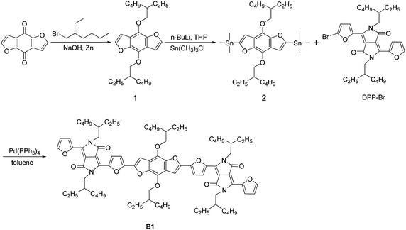 |
| | Scheme 1 Synthetic routes of the compounds and B1. | |
Optical properties
The photo-physical properties of B1 can be obtained through the test of ultraviolet-visible spectrum. The absorption spectrum of B1 is shown in Fig. 1. In the solution state, B1 has an optical absorption between 350–750 nm, and the maximum absorption peak is about 630 nm. In the film state, B1 shows two main absorption regions, 350–420 nm, which are caused by the π–π* transition on the main chain of B1. While the absorption region of 500–750 nm, it is due to the absorption of charge transfer between the DPP acceptor unit and the BDF donor unit. Compared with the solution state, the absorption edge in the film state has a significant red shift, mainly due to the stronger interaction between B1 molecules in the film state.21 According to the onset absorption of the B1 film, the corresponding optical band gap can be calculated to be 1.65 eV.
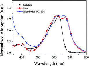 |
| | Fig. 1 Normalized absorption spectra of B1 in solution and film state. | |
Electrochemical properties
The family of square wave voltammetry (SWV) curves obtained for B1 of study is presented in Fig. 2. The potential difference between HOMO peak (the half wave potential of anodic process) and LUMO peak illustrates the electrochemical band-gaps for corresponding small molecules. Due to the absorption of incident photons with energies larger than band-gaps of the material of active layer, the electrons of HOMO of donor will be excited up to LUMO leaving a positive charge on the HOMO. If the LUMO level of acceptor is lower than the LUMO level of donor, the excited electrons will be transferred to acceptor resulting in a charge separation of the electron–hole pair. The difference between LUMO levels of donor and acceptor of roughly 0.3 eV is expected to yield optimum charge separation and recombination prevention.22
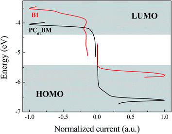 |
| | Fig. 2 Square wave voltammetry of B1 and acceptor material PC61BM. | |
The potential difference between the peaks of LUMO of acceptor and HOMO of donor reflects the Voc of the devices assembled from the corresponding materials. The HOMO and LUMO levels of B1 are −5.76 eV and −3.51 eV, respectively. The electrochemical band gap of B1 is the difference between the HOMO and LUMO energy levels, which is 2.25 eV. The electrochemical band gap of B1 is significantly higher than the optical band gap, which may be caused by the interface impedance during charge injection.23
DFT calculations
Using the method of DFT B3LYP/6-31G* in Gaussian 03 software, the HOMO and LUMO energy levels of the compound were calculated to further optimize the structure. In order to simplify the calculation, this paper replaces the alkyl chain with methyl, and uses the DFT/B3LYP/6-31G* method to obtain the optimal geometric configuration and electronic arrangement in the molecular system. From the Ab intitio results of B1 model molecule (Fig. 3), it can be seen that the electron delocalization in the entire molecule is caused by p-conjugation. The HOMO and LUMO energy levels of B1 are calculated using the DFT/B3LYP/6-31G* method, which are −5.69 and −3.50 eV, respectively, and the corresponding energy gap is 2.19 eV, which is in good agreement with the experimental results. From these studies, we conclude that the DFT calculation method can quickly and accurately determine the HOMO, LUMO energy level and band-gap of the organic small molecules.
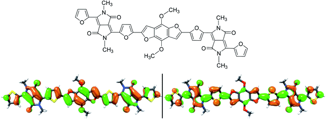 |
| | Fig. 3 HOMO (left) and LUMO (right) energy levels of B1. | |
Organic solar cells
In order to study the photovoltaic performance of B1, we adopted the bulk heterostructure ITO/PEDOT:PSS/B1:C61BM/LiF/Al. Fig. 4 shows the J–V curve of B1 under AM1.5G, 100 mW cm−2, and the corresponding open circuit voltage (Voc), short circuit current (Jsc) and fill factor (FF) are summarized in Table 1. B1 is blended with PC61BM in proportions of 1:0.5, 1:1, and 1:2 to optimize the photovoltaic performance of the devices. When B1 is blended with PC61BM in a 1:1 ratio, the best power conversion efficiency (PCE) is obtained, which is 1.7%, the corresponding Voc is 0.87 V, Jsc is 5.8 mA cm−2, and FF is 0.34. After when we processed the photovoltaic active layer by thermal annealing, the PCE was significantly improved to 5.0%, the corresponding Voc is 0.82 V, Jsc is 11.1 mA cm−2, and FF is 0.56. These results indicate that thermal annealing effectively improves the photovoltaic performance of the devices.
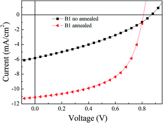 |
| | Fig. 4 J–V curves of the PSCs based on B1/PC61BM under illumination of AM1.5G, 100 mW cm−2. | |
Table 1 Photovoltaic parameters of the OSCs based on B1/PC61BM
| Active layer |
Voc (V) |
Jsc (mA cm−2) |
FF (%) |
PCE (%) |
μhole (cm2 V−1 s−1) |
| As-cast devices. With thermal annealing at 120 °C for 10 min. The average values for the B1-based PSCs are obtained from 12 devices. Hole mobility from space charge limit current (SCLC). |
| B1:PC61BM = 1:1a |
0.87 (0.86 ± 0.02)c |
5.8 (5.9 ± 0.1)c |
34.0 (33.5 ± 1.2)c |
1.7 (1.8 ± 0.2)c |
3.4 × 10⁻³d |
| B1:PC61BM = 1:1b |
0.82 (0.84 ± 0.03)c |
11.1 (11.3 ± 0.4)c |
55.5 (56.1 ± 1.5)c |
5.0(4.9 ± 0.1)c |
7.7 × 10⁻²d |
We reconfirmed the accuracy of the J–V test results through the external quantum conversion efficiency (EQE). Under the same test conditions as the current–voltage curve (J–V), we tested the EQE performance of the photovoltaic device, as shown in Fig. 5. In solar cells, obtaining high external quantum conversion efficiency means obtaining high Jsc. From the results of EQE, it can be concluded that the photovoltaic results are accurate. The EQE value of B1 reached more than 40% in the 350–700 nm range, the corresponding current is 11.4 mA cm−2.
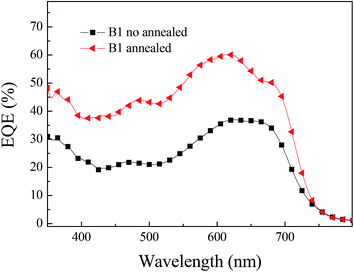 |
| | Fig. 5 The EQE curves of the PSCs based on B1/PC61BM. | |
Photoluminescence
The quenching efficiency of photoluminescence (PL) upon the addition of fullerene is usually considered to reflect the possibility of exciton dissociation at donor/acceptor interface within their lifetime.24 We tested the photoluminescence based on pure B1 film, B1:PC61BM film and B1:PC61BM film after thermal annealing. As shown in Fig. 6, we can intuitively study the charge transfer and exciton dissociation in the film by photoluminescence. When the B1 film is excited by the light source, the electrons jump from the ground state to the excited state, the electrons in the excited state are unstable and return to the ground state by emitting fluorescence. Therefore, the fluorescence peak of B1 is located at 780 nm. As B1:PC61BM film, the electrons in the single excited state of B1 can not only emit fluorescence, but also transfer the charge to the excited state of the acceptor PC61BM, which causes the fluorescence emission of B1 to be quenched. Based on B1:PC61BM device, the fluorescence quenching rate is 78%, and B1:PC61BM device after thermal annealing, the fluorescence quenching rate is increased to 86%. Based on the above analysis, it is shown that the thermally annealed devices have higher charge transfer and exciton dissociation efficiency. This facilitates exciton dissociation, and is in agreement with the high photocurrents obtained in the solar cells measurements.
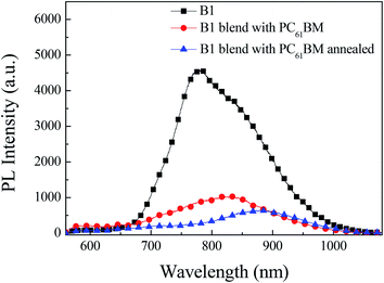 |
| | Fig. 6 Photoluminescence spectra of pure B1films, B1:PC61BM blend films prepared without and with thermal annealing. | |
Morphology
The morphology of the active layer at the nanometer size also plays an important role in the performance of the photovoltaic device. Appropriate morphology is not only conducive to the separation of excitons, but also conducive to the transfer of charges to the respective electrodes and effective collection. In order to better explain the solar cell in B1:PC61BM (1:1, w/w), the best photovoltaic efficiency is obtained after thermal annealing, we used atomic force microscope (AFM) to study the surface morphology of the blend film. From the height image (Fig. 7), the root-mean-square (rms) roughness values of the blend films for B1 are 0.53 and 0.80 nm for before and after thermal treatment, respectively. When the active layer is annealed, the surface roughness is significantly improved. The active layer exhibits a nano-level phase separation morphology, which promotes the effective separation and transport of carriers, and the short-circuit current is significantly improved, resulting in higher power conversion efficiency.25
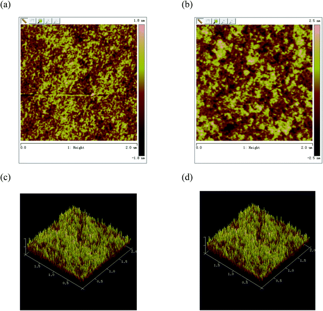 |
| | Fig. 7 AFM images of B1:PC61BM (1:1, w/w) blend films spin coated from CHCl3: (a) and (c) without annealing phase image and height image; (b) and (d) with annealing phase image and height image. | |
Conclusions
In summary, a new type of narrow band gap DPP-based organic electron donor B1 was synthesized by Stille coupling reaction. B1 shows a broad absorption spectrum. When B1:PC61BM without any post-processing, the PCE is lower, mainly due to the low short-circuit current and low fill factor. After the photovoltaic active layer was annealed at 120 °C for 20 minutes, the power conversion efficiency increased from 1.7% to 5.0%. The increase of PCE is mainly due to the improvement of the morphology of the active layer by thermal annealing, thereby promoting the charges separation and transmission. These results indicate that B1 is an organic donor material for high-efficiency solar cells.
Conflicts of interest
There are no conflicts to declare.
Acknowledgements
The work was supported by the National Natural Science Foundation of China (21604022, 51703062), the Natural Science Foundation of Hunan Provincial (2019JJ50408, 2018JJ3370 and 2020JJ4444), Huxiang Youth Talent Support Program (2018RS3147), PhD startup project of Hunan University of Arts and Science (15BSQD09).
Notes and references
- J. E. Coughlin, Z. B. Henson, G. C. Welch and G. C. Bazan, Acc. Chem. Res., 2014, 47, 257 CrossRef CAS.
- Y. Li, Acc. Chem. Res., 2012, 45, 723 CrossRef CAS.
- Z. Hu, L. Ying, F. Huang and Y. Cao, Sci. China: Chem., 2017, 60, 571 CrossRef CAS.
- B. Kan, M. Li, Q. Zhang, F. Liu, X. Wan, Y. Wang, W. Ni, G. Long, X. Yang, H. Feng, Y. Zuo, M. Zhang, F. Huang, Y. Cao, T. P. Russell and Y. Chen, J. Am. Chem. Soc., 2015, 137, 3886 CrossRef CAS.
- O. P. Lee, A. T. Yiu, Pi. M. Beaujuge, C. H. Woo, T. W. Holcombe, J. E. Millstone, J. D. Douglas, M. S. Chen and J. M. J. Fréchet, Adv. Mater., 2011, 23, 5359 CrossRef CAS.
- Q. Shi, P. Cheng, Y. Li and X. Zhan, Adv. Energy Mater., 2011, 2, 63 CrossRef.
- Q. Hou, Y. Chen, H. Zhen, Z. Ma, W. Hong, G. Shi and F. Zhang, J. Mater. Chem. A, 2013, 1, 4937 RSC.
- G. Zhang, J. Zhao, P. C. Y. Chow, K. Jiang, J. Zhang, Z. Zhu, J. Zhang, F. Huang and H. Yan, Chem. Rev., 2018, 118, 3447 CrossRef CAS.
- E. Ripaud, T. Rousseau, P. Leriche and J. Roncali, Adv. Energy Mater., 2011, 1, 540 CrossRef CAS.
- S. Ma, Y. Fu, D. Ni, J. Mao, Z. Xie and G. Tu, Chem. Commun., 2012, 48, 11847 RSC.
- R. Fitzner, C. Elschner, M. Weil, C. Uhrich, C. Körner, M. Riede, K. Leo, M. Pfeiffer, E. Reinold, E. Mena-Osteritz and P. Bäuerle, Adv. Mater., 2012, 24, 675 CrossRef CAS.
- D. H. Wang, A. Kyaw, V. Gupta, G. C. Bazan and A. J. Heeger, Adv. Energy Mater., 2013, 3, 1161 CrossRef CAS.
- J. Huang, C. Zhan, X. Zhang, Y. Zhao, Z. Lu, H. Jia, B. Jiang, J. Ye, S. Zhang, A. Tang, Y. Liu, Q. Pei and J. Yao, ACS Appl. Mater. Interfaces, 2014, 6, 3853 CrossRef CAS.
- T. S. Poll, J. A. Love, T. Q. Nguyen and G. C. Bazan, Adv. Mater., 2012, 24, 3646 CrossRef.
- Y. Lin, L. Ma, Y. Li, Y. Liu, D. Zhu and X. Zhan, Adv. Energy Mater., 2013, 3, 1166 CrossRef CAS.
- Y. Zou, D. Gendron, R. Neagu-Plesu and M. Leclerc, Macromolecules, 2009, 42, 6361 CrossRef CAS.
- S. Loser, C. J. Bruns, H. Miyauchi, R. P. Ortiz, A. Facchetti, S. I. Stupp and T. J. Marks, J. Am. Chem. Soc., 2011, 133, 8142 CrossRef CAS.
- L. Huo, L. Ye, Y. Wu, Z. Li, X. Guo, M. Zhang, S. Zhang and J. Hou, Macromolecules, 2012, 45, 6923 CrossRef CAS.
- B. Liu, B. Qiu, X. Chen, L. Xiao, Y. Li, Y. He, L. Jiang and Y. Zou, Polym. Chem., 2014, 5, 5002 RSC.
- X. Chen, B. Liu, Y. Zou, L. Xiao, X. Guo, Y. He and Y. Li, J. Mater. Chem., 2012, 22, 17724 RSC.
- C. Cui, J. Min, C. Ho, T. Ameri, P. Yang, J. Zhao, C. Brabec and W. Wong, Chem. Commun., 2013, 49, 4409 RSC.
- Z. Tang, L. M. Andersson, Z. George, K. Vandewal, K. Tvingstedt, P. Heriksson, R. Kroon, M. R. Andersson and O. Inganäs, Adv. Mater., 2012, 24, 554 CrossRef CAS.
- B. Liu, X. Chen, Y. Zou, L. Xiao, X. Xu, Y. He, L. Li and Y. Li, Macromolecules, 2012, 45, 6898 CrossRef CAS.
- D. Qian, B. Liu, S. Wang, S. Himmelberger, M. Linares, M. Vagin, C. Müller, Z. Ma, S. Fabiano, M. Berggren, A. Salleo, O. Inganäs, Y. Zou and F. Zhang, J. Mater. Chem. A, 2015, 3, 24349 RSC.
- J. A. Love, C. M. Proctor, J. Liu, C. J. Takacs, A. Sharenko, T. S. Poll, A. J. Heeger, G. C. Bazan and T. Q. Nguyen, Adv. Funct. Mater., 2013, 23, 5019 CrossRef CAS.
Footnote |
| † Electronic supplementary information (ESI) available: Synthetic details for B1, characterization methods, the OSCs fabrication details, figures showing J–V curves, the photovoltaic data are summarized in Table S1. See DOI: 10.1039/d0ra07415b |
|
| This journal is © The Royal Society of Chemistry 2020 |
Click here to see how this site uses Cookies. View our privacy policy here. 
 Open Access Article
 This Open Access Article is licensed under a Creative Commons Attribution-Non Commercial 3.0 Unported Licence
 *ab,
Xiaobo Wangab,
Lang Lic and
Gang Wang*ab
*ab,
Xiaobo Wangab,
Lang Lic and
Gang Wang*ab


