
 Open Access Article
 This Open Access Article is licensed under a Creative Commons Attribution-Non Commercial 3.0 Unported Licence
Low-temperature operating ZnO-based NO2 sensors: a review
Jingyue Xuan,
Guodong Zhao,
Meiling Sun,
Fuchao Jia ,
Xiaomei Wang,
Tong Zhou,
Guangchao Yin* and
Bo Liu*
,
Xiaomei Wang,
Tong Zhou,
Guangchao Yin* and
Bo Liu*
Laboratory of Functional Molecular and Materials, School of Physics and Optoelectronic Engineering, Shandong University of Technology, Zibo 255000, China. E-mail: yingc@sdut.edu.cn; liub@sdut.edu.cn; Fax: +86 533 2783909
First published on 30th October 2020
Abstract
Owing to its excellent physical and chemical properties, ZnO has been considered to be a promising material for development of NO2 sensors with high sensitivity, and fast response and recovery. However, due to the low activity of ZnO at low temperature, most of the current work is focused on detecting NO2 at high operating temperatures (200–500 °C), which will inevitably increase energy consumption and shorten the lifetime of sensors. In order to overcome these problems and improve the practicality of ZnO-based NO2 sensors, it is necessary to systematically understand the effective strategies and mechanisms of low-temperature NO2 detection of ZnO sensors. This paper reviews the latest research progress of low-temperature ZnO nanomaterial-based NO2 gas sensors. Several efficient strategies to achieve low-temperature NO2 detection (such as morphology modification, noble metal decoration, additive doping, heterostructure sensitization, two-dimensional material composites, and light activation) and corresponding sensing mechanisms (such as depletion layer theory, grain boundary barrier theory, spill-over effects) are also introduced. Finally, the challenges and future development directions of low-temperature ZnO-based NO2 sensors are outlined.
1. Introduction
In modern life, the development of industrialization and urbanization has resulted in a tremendous increase in air pollution. Particularly, nitrogen dioxide (NO2) is a toxic gas with a pungent odor that directly causes the deterioration of human health when exposed to ppm levels of NO2. In addition, NO2 is also one of the causes of acid rain, bringing various environmental effects such as reduced visibility in the atmosphere and acidification of surface water. Therefore, it is essential to develop a gas sensor for the real-time detection and emission control of NO2.1–4For decades, metal oxide semiconductors (MOSs), including ZnO,5,6 CuO,7–9 SnO2,10–12 TiO2,13–15 Fe2O3,16,17 In2O3,18,19 and WO3,20,21 have dominated the field of toxic gas detection (including NO2 detection) nanomaterials, because of their low-cost, non-toxicity and availability.22–27 Among these materials, ZnO have been witnessed an immense exploration due to its wide band gap, large exciton binding energy, high mobility of conduction electrons, physical and chemical stability.28–30 Recently, ZnO-based gas sensors with different nanostructures (nanowires, nanorods, nanosheets, quantum dots, etc.) have been widely reported.31–35 Although improved preparation methods and modified morphologies have significantly enhanced gas sensing performance of ZnO-based sensors,36–42 the most reported sensors still operated at high temperatures, which limited their practical applicability. Owing to ZnO-based gas sensors generally need to be heated the sensing layer to a higher temperature (300–500 °C) to achieve the sensing performance, leading to a high-power consumption and changes in the nanomaterial microstructure.43–47 The limitation of high-temperature sensing is also reflected in the detection of flammable and explosive gases, with a risk of explosion.48 In addition, it was found that the decrease of oxygen ions adsorbed on the surface of the gas-sensing materials would result in the decrease of the response value of sensors when the operating temperature is too high.49 Out of consideration for the safety and stability, sensors that can work at lower temperatures are becoming more and more desirable. Achieving this requirement can not only reduce energy consumption and cost, but also improve the accuracy of the detection results. Therefore, a systematic understanding of strategies of preparing low-temperature ZnO-based NO2 sensors and the corresponding sensing mechanisms is of guiding significance for the design of novel low-temperature ZnO-based NO2 sensors.
To the best of our knowledge, several review papers have been published for ZnO-based gas sensors.42,50 However, most of these review articles discuss the characteristics of sensors at high operating temperatures. Recently, some reviews on ZnO-based gas sensors at low operating temperatures have been reported. For instance, S. Kumar et al. have reported the new development of NO2 gas sensor based on metal oxide nanostructures, which focus on the discussion of the structure of ZnO nanowires.30 Zhu et al. addressed the room-temperature sensing performance of ZnO-based gas sensors, but a specific discussion on the sensing mechanism of NO2 was lacking.51 Zhang et al. presented the main strategies for modifying metal oxides based room-temperature NO2 sensor without a targeted discussion of ZnO sensing materials.52 R. Kumar et al. summarized the application of photoactivation in the field of ZnO-based gas sensors.47 Li et al. emphasized the designs and mechanisms of semiconductor oxides of different patterns for room-temperature gas sensors.48 Srinivasan et al. discussed the development status of room-temperature gas sensors for different inorganic gases and volatile organic compounds.53 Nevertheless, until now it is still lack of a comprehensive review of the latest developments in ZnO-based gas sensors for NO2 detection at low operating temperatures. Therefore, this review will summarize and discuss the latest reports on various technologies that can be used to improve the gas-sensing properties of ZnO for NO2 at low operating temperatures, including surface morphological modification, noble metal decoration, functionalization of additive doping, inorganic heterojunction sensitization, light activation and so on. In addition, the gas-sensing mechanism will be briefly discussed and the future development of ZnO-based gas sensors will be outlined.
2. Gas sensing mechanism of NO2
Towards the most common gas sensors, chemical-resistance type sensors, their gas-sensing mechanism is directly related to the electron exchange generated by the oxidation–reduction reaction between the surface electrons of the material and the target gas. Specifically, in the air atmosphere, oxygen molecules as electron acceptors are chemically adsorbed on the surface of the ZnO materials (eqn (1)).54–56 By trapping electrons from the ZnO conduction band, oxygen molecules ionize on the surface of the material to form oxygen ions. Therefore, an electron-depleted space-charge layer appears on the surface of ZnO, and a potential barrier is formed due to the decrease of electron density, which leads to a reduction of the electron conduction of ZnO and an increase in resistance.57 This is called the reference resistance in air. The type of oxygen species adsorbed (O2−, O−, O2−) depends on the operating temperature, as can be observed on the reaction in eqn (2)–(4).58| O2(gas) → O2(ads) | (1) |
| O2(ads) + e− → O2−(ads), T < 100 °C | (2) |
| O2−(ads) + e− → 2O−(ads), 100 °C < T < 300 °C | (3) |
| O−(ads) + e− → O2−(ads), T > 300 °C | (4) |
The sensors studied in this review operate at low temperatures (T < 200 °C). When the sensor is exposed to the oxidizing gas such as NO2, the gas molecules will not only capture the electrons in the conduction band of ZnO, but also interact with the oxygen species adsorbed on the surface of ZnO, resulting in an increase in the width of the electron depletion layer and junction potential barriers, which will increase the resistance of sensor and generate sensing response (eqn (5)–(7)).59–61 When the sensor is exposed to air again, NO2− reacts with the holes and releases the electrons back to the conduction band, causing NO2 to be released into the air and reducing the resistance (eqn (8)). Fig. 1 schematically shows the sensing mechanism of a ZnO-based gas sensor in the NO2 gas atmosphere at room temperature.1
| NO2(gas) + e− → NO2−(ads) | (5) |
| NO2−(ads) + O2−(ads) + e− → 2O−(ads) + NO2−(ads), T < 100 °C | (6) |
| NO2−(ads) + O−(ads) + 2e− → 2O2−(ads) + NO(gas), 100 °C < T < 300 °C | (7) |
| NO2−(ads) + h+ → NO2(gas) | (8) |
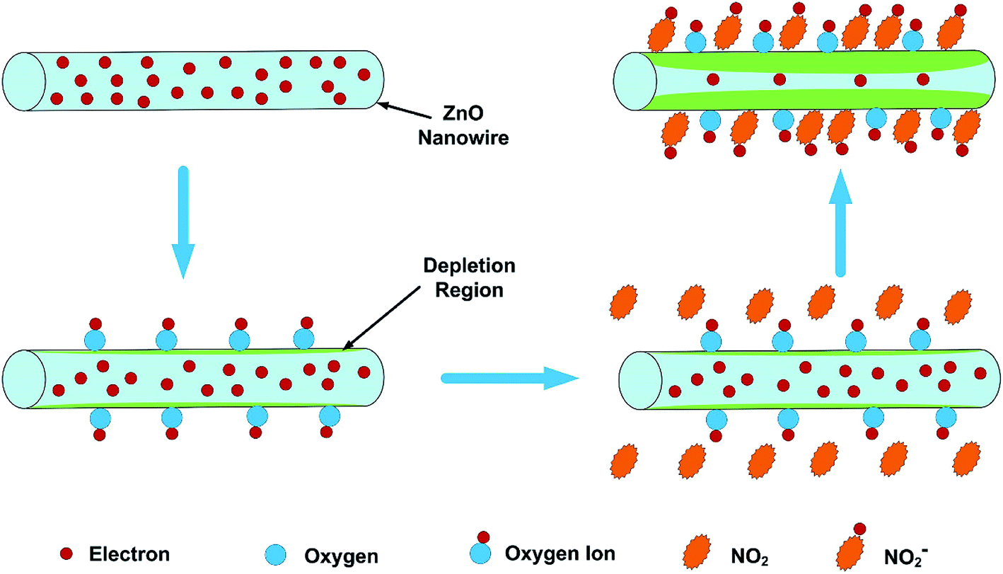 | ||
| Fig. 1 Schematic diagram of the sensing mechanism of the ZNW arrays to NO2. This figure has been reproduced with permission from ref. 1, Elsevier, Copyright 2018 (License Number: 4923970909803). | ||
The above reactions are the essence of the gas-sensing signal. How to reduce the operating temperature and improve the gas-sensing performance is usually related to the speed and difficulty of the above-mentioned reactions. Next, we will introduce several effective strategies for achieving low-temperature NO2 detection and discuss the corresponding reaction mechanism.
3. Efficient ways to achieve low-operating temperature NO2 detection
3.1. Surface morphological modification
The grain size, porosity, and surface state of ZnO have a significant impact on the performance of sensor via increasing the proportion of electron depletion layer in the entire materials. Based on the above mechanisms, ZnO nanomaterials can form electron depletion region with thickness of one Debye length on their surface after reacting with oxygen in the air. When the particle size (or diameter) of ZnO nanomaterials is less than twice the Debye length, the entire nanomaterials will become electron depletion region, that is, the entire nanomaterial can exchange electrons, not just on the surface.62 This time, the response of sensor usually increase significantly as the particle size decreases. But blindly reducing the grain size will also promote particle agglomeration and reduce the size of the exposed specific surface area.63 Therefore, adjusting optimal grain size, avoiding the materials agglomeration, promoting gas diffusion and their synergy effects are keys to achieve low-operating temperature gas response. Besides, the surface defects of ZnO nanostructures such as oxygen vacancies are also important for the gas-sensing performance of ZnO. Oxygen vacancies are regarded as reactive oxygen species, and the unpaired electrons present in ZnO can serve as active sites for gas-sensing reactions, which will enhance gas adsorption and dissociation, as well as promote subsequent redox reactions.64–66Up to now, ZnO with different morphologies have been designed to achieve room-temperature gas-sensitivity through various routes. Different spatial structures lead to different gas diffusion capacities during the adsorption–desorption process of gas molecules. For example, one-dimensional (1D) nanowires, nanorods, nanotubes, nanofiber structures, two-dimensional (2D) nanosheets, nanoflakes have high surface-to-volume ratio, leading to greater electron depletion.67–71 This characteristic accelerates the surface reaction, reduces the operating temperature, and finally achieves gas-sensing at low-operating temperatures. For instance, Xia et al. synthesized nanorods with different diameters through a simple nanoseed-assisted method.72 Compared with submicron ZnO rods with a diameter of 0.5–1.00 mm, ultrathin nanorods with a diameter of 4–10 nm show more sensitive detection of NO2 at room temperature. This is because they have large channel conduction changes to the channel diameter. Yan et al. compared the NO2 sensing performance of high-density ZnO nanosheets and nanorods grown onto porous silicon (PS) substrate.73 At room temperature, the nanosheets/PS sensor with the thickness around 10 μm and average pore sizes about 1.5 μm shows a better response and gas sensitivity, as well as much better response–recovery characteristics to NO2 gas. Owing to the large specific surface area, the nanosheets have more active sites among them, which can effectively improve the response ability.
Obviously, the porous structure with pore size or high porosity is one of the most promising structures, owing to its more diffusion channels. For example, Chen et al. reported mesoporous ZnO sheets assembled by the calcination of nanoparticles. The size of the nanoparticles of the sample falls into different ranges at different calcination temperatures.74 After characterization by the use of nitrogen adsorption technique, the average particle size of the assembled nanosheets synthesized at a calcination temperature of 100 °C is the smallest (5–10 nm) and the specific surface area is the largest (87.63 m2 g−1). At the same time, the mesoporous ZnO nanosheets obtained by calcination at 100 °C exhibited excellent NO2 response performance at room temperature (Fig. 2a–c), and the response to 1 ppm NO2 is 135%. The authors attribute the excellent room-temperature gas-sensing performance of mesoporous ZnO nanosheets calcined at 100 °C to the high specific surface area and hollow structure. Based on the surface depletion model (Fig. 2d), smaller nanoparticles enhance the radial modulation of the conduction channel in NO2 sensing applications, resulting in enhanced sensing performance. Xia et al. reported a room-temperature NO2 gas sensor using macro-/mesoporous ZnO films.75 This gas sensor exhibits an ultra-high response value of 2900% to 1000 ppb NO2 at room temperature. Moreover, the sensor shows full reversibility, sub-ppb detection limit (0.2 ppb) and high selectivity to NO2.
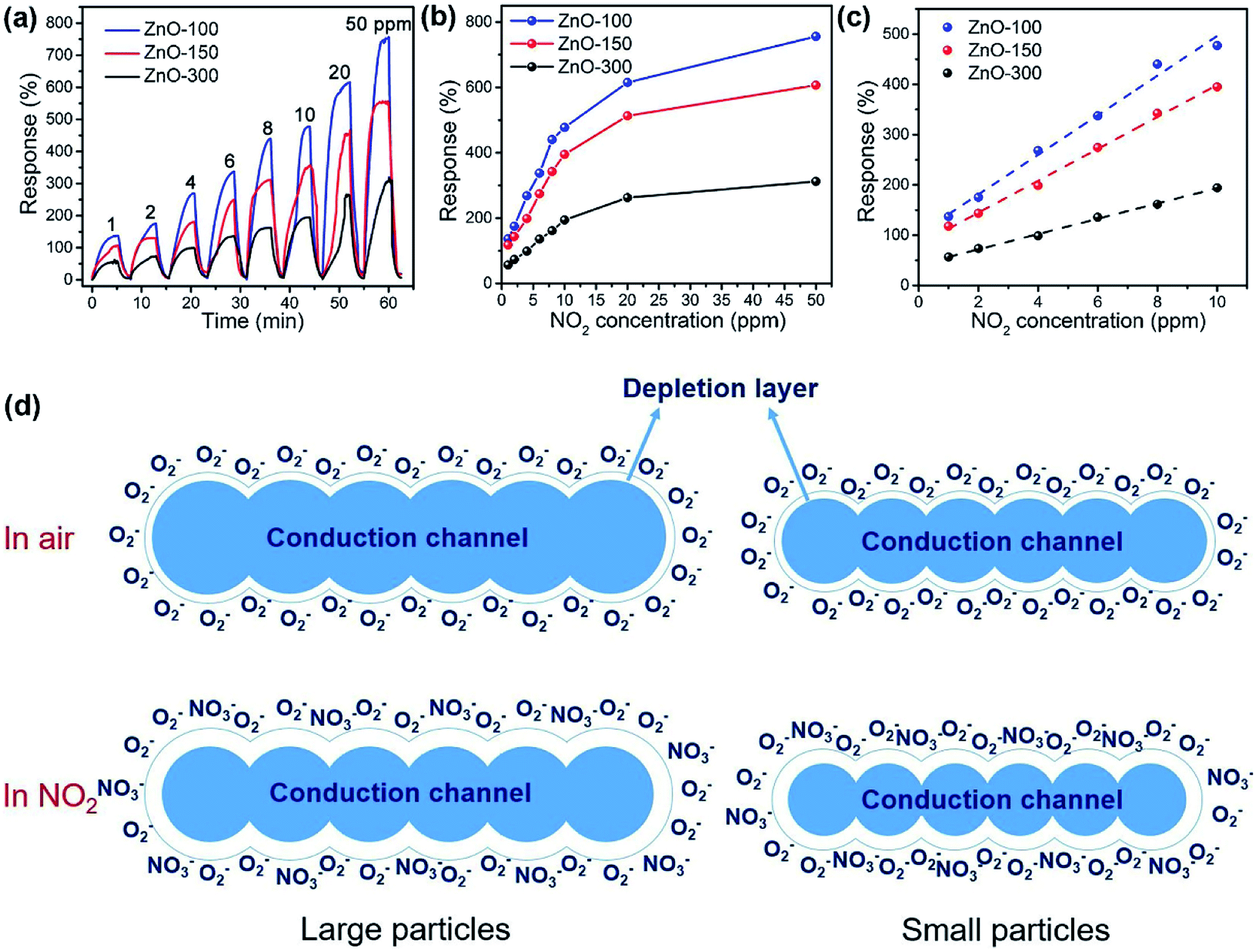 | ||
| Fig. 2 (a) Dynamic response curves and responses (b) of the sensors based on the ZnO-100, ZnO-150 and ZnO-300 samples to 1–50 ppm of NO2 at room temperature; (c) fitting curves of response vs. NO2 concentration in the range of 1–10 ppm of NO2. (d) Schematic illustration of the changes in the conduction channel of the mesoporous ZnO sheets assembled by large and small nanoparticles upon exposure to NO2. This figure has been reproduced with permission from ref. 74, Elsevier, Copyright 2018 (License Number: 4923980499171). | ||
In addition, some researchers have also been able to enhance the gas-sensing properties by modulating the surface defects of ZnO. Yu et al. used facial solution method with subsequent annealing to prepare ZnO nanowalls.76 The nanowalls annealed at 450 °C for 1 h exhibit 6.5 of response value to 50 ppm NO2 and fast response/recovery times (23/11 s) and good repeatability. The combination of defects and morphology analyses results based on the photoluminescence (PL) and scanning electron microscope (SEM) characterizations show that oxygen vacancies defects and porosity facilitate NO2 gas sensing response in ZnO nanowalls at room temperature. Another gas sensor made of porous ZnO polygonal nanoflakes prepared using a microwave hydrothermal method combined with a subsequent annealing process also exhibits an excellent response with a value of 134 to 1 ppm NO2 at 175 °C.77 The results prove that the different gas-sensitivity characteristics of samples obtained at different calcination temperatures depend on the crystal defects. The PL spectra and the X-ray photoelectron spectroscopy (XPS) spectra further prove that the oxygen vacancies and surface oxygen species are crucial for the excellent sensing performance. Table 1 provides a brief comparative study on different morphologies of ZnO for NO2 detection at low temperatures.
| Morphology | NO2 concentration | Temperature (°C) | Response | Response and recovery time | Ref. |
|---|---|---|---|---|---|
| Mesoporous sheets | 1 ppm | RT |  |
3/5 min | 74 |
| Nanorods | 1 ppm | RT |  |
— | 72 |
| Nanosheets | 1 ppm | RT | 5.75 (Ra/Rg) | 200/180 s | 73 |
| Nanowalls | 50 ppm | RT | 6.5 (Rg/Ra) | 23/11 s | 76 |
| Nanoflakes | 1 ppm | 175 °C | 134 (Rg/Ra) | — | 77 |
| Macro-/mesoporous films | 400 ppb | RT |  |
19/32 s | 75 |
3.2. Functionalization of noble metal nanoparticles
In gas-sensing applications, the sensors have been widely studied for achieving gas detection at low temperatures via functionalization of noble metal nanoparticles (e.g. Au,78 Pt,79 Pd,80 Ag81) on the surface of ZnO. There are two sensitization mechanisms involved, namely chemical sensitization mechanism and electronic sensitization mechanism.82 The chemical mechanism is based on the spill-over effect. Under this effect, noble metal nanoparticles exist on the surface of ZnO as catalysts, which enhances the adsorption of oxygen molecules and activates their dissociation, causing the spill-over of products onto ZnO.83,84 In addition, NO2 gas can also be adsorbed on noble metal nanoparticles and then migrate to ZnO surface to react with oxygen ions through the spill-over effect, which leads to faster adsorption of oxygen and NO2 gas. This effect not only reduces the operating temperature of ZnO-based sensor, but also improves its sensing performance.In the case of the electronic mechanism, since the work function of the noble metal is larger than that of ZnO, electrons are transferred from the ZnO to the noble metal nanoparticles.85–87 As a consequence, a band bend occurs at the interface of the noble metal and ZnO, forming a nano-Schottky barrier.88–90 When exposed to NO2, the electrons will be further depleted, increasing the depletion layer width and resistance of sensor. Furthermore, noble metal nanoparticles as well accelerate the transfer of electrons on the surface of ZnO. Therefore, the synergistic effects of chemical sensitization and electronic sensitization achieve excellent performance of sensor operating at low-temperature. Table 2 displays a comparison of gas sensing response based on functionalized noble metal nanoparticles/ZnO nanostructures at low operating temperatures.
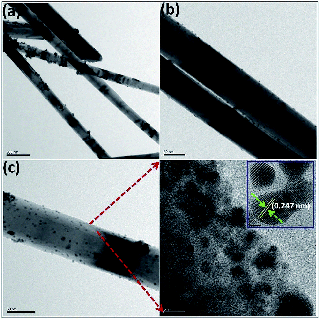
Chen et al. prepared Pd nanoparticles (1, 2, 5 mol%) functionalized ZnO nanowires (Pd-ZNWs) by a convenient hydrothermal method.91 The high-resolution transmission electron microscopy (HRTEM) images show that the obtained Pd-ZNWs have a length of 2 μm, a diameter of 150 nm, and Pd/PdO nanoparticles with a size of 2–5 nm distributed on the surface of the ZNWs. When pure ZNWs and Pd-ZNWs are exposed to 1 ppm NO2 at 100 °C, the response and recovery times of Pd-ZNWs are much shorter than of pure ZNWs. As shown in Fig. 3, the maximum response value of pure ZNWs to 1 ppm NO2 is 8.2 at 150 °C. Compared with that, the optimal operating temperature of the Pd-ZNWs reduce to 100 °C. At the same NO2 concentration, the response value of 1 mol% Pd-ZNWs increased by 1.65 times. The selective response of Pd-ZNWs to CO, NH3, H2, SO2 and some volatile organic compounds (VOC) was studied. The result demonstrates that Pd-ZNWs is highly selective for NO2 gas. Under the synergistic effects of electronic sensitization and chemical sensitization of surface-functionalized Pd NPs, the working temperature of sensor is reduced and the gas-sensing characteristics of NO2 are enhanced (Fig. 3e).
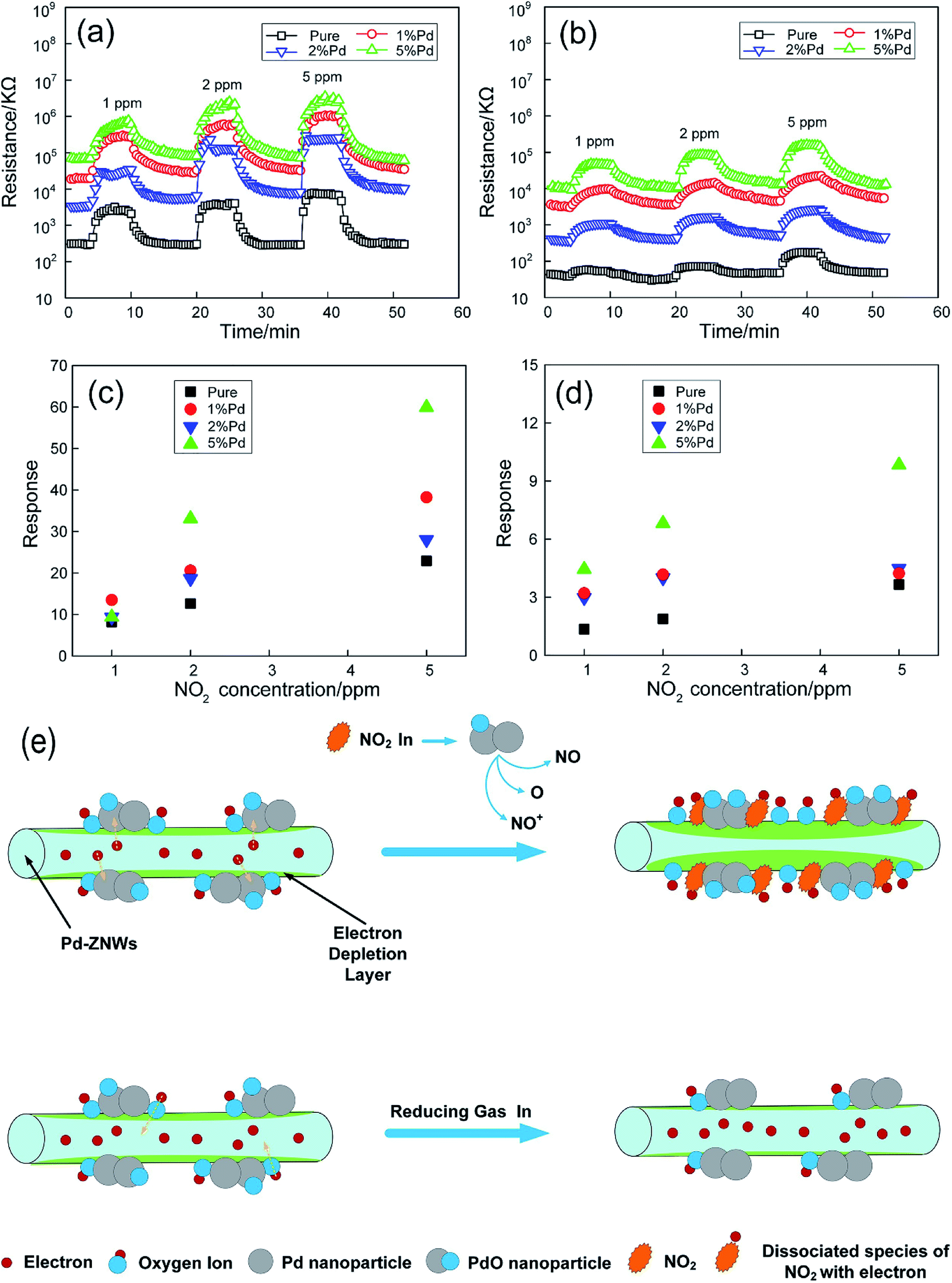 | ||
| Fig. 3 Dynamic responses of the sensors based on pure (@150 °C) and Pd-ZNWs (@100 °C) upon exposure to NO2 gas with various concentrations at (a) 30% RH and (b) 60% RH. The corresponding sensor responses as a function of NO2 concentration at (c) 30% RH and (d) 60% RH. (e) Sensing mechanisms of Pd-ZNWs towards NO2 and reducing gas. This figure has been reproduced with permission from ref. 91, Elsevier, Copyright 2019 (License Number: 4923990843354). | ||
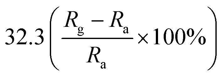
An ultralong ZnO@Au heterojunction NRs-based gas sensor was prepared using a facile wet-chemical approach via in situ reduction process by Dinesh et al.93 As shown in Fig. 4, the Au nanoclusters with an average particles size of 4.5 ± 0.25 nm are uniformly distributed along on the ZnO NRs (length around 30 μm and diameter around 60 nm). The micro Raman studies suggest that the presence of ZnO@Au heterojunction is conducive to form a larger barrier and tends to the highest response. The sensor has a super-high response value of 400 to 5 ppm NO2 at a lower temperature (150 °C). It also shows good selectivity, compared to other gases including NH3, H2S, ethanol, acetone. Namgung and co-workers achieved room-temperature NO2 sensing performance from Al-doped ZnO nanorod/silver nanowire (AZO NRs/AgNWs) bilayer sensor.94 The AZO NRs were synthesized through wet ZnO NR growth, Al sputtering, and thermal drive-in diffusion, and AgNWs were then introduced by drop-casting. The sensor (AZO NRs and AgNWs film with a weight ratio of 3![[thin space (1/6-em)]](https://www.rsc.org/images/entities/char_2009.gif) :2) exhibits a response of 32.3% to 10 ppm NO2. This improvement is attributed to the synergistic interplay of Al-doped ZnO nanorods and silver nanowires.
:2) exhibits a response of 32.3% to 10 ppm NO2. This improvement is attributed to the synergistic interplay of Al-doped ZnO nanorods and silver nanowires.
 | ||
| Fig. 4 (a–c) TEM and (d) HRTEM images of UL ZnO@Au heterojunction NRs, (inset showing the HRTEM image of Au). This figure has been reproduced with permission from ref. 93, Elsevier, Copyright 2017 (License Number: 4924050884483). | ||
In addition, the bimetallic NPs exhibit better physical and chemical properties than individual metals due to synergistic effects. Chen et al. loaded bimetallic Au/Pd nanoparticles (NPs) on ZnO nanowires (ZNWs) by a simple dipping process with heating evaporation.92 By comparing with the pristine ZNWs and the counterparts of single Au- or Pd-NPs decorated ZNWs, ZNWs decorated with bimetallic Au/Pd NPs reduce the optimal operating temperature to 100 °C and obtain the optimal gas-sensing response. The sensitization synergistic effects of bimetallic Au/Pd NPs and the increase of oxygen vacancies enhance the sensing performance.
3.3. Additive doping
It is worth noting that low-temperature gas-sensing based on ZnO gas sensors can also be achieved by adding dopants such as metals, conductive polymers to the ZnO nanostructures. Table 3 displays a part reports about low-temperature gas sensing properties of dopant/ZnO. In this section, we will summarize the mechanisms of metal addition and conductive polymer addition, respectively.| Dopant | Morphology (ZnO) | NO2 concentration | Temperature (°C) | Response | Response and recovery time | Ref. |
|---|---|---|---|---|---|---|
| Cu | Nanorods | 1 ppm | 175 °C |  |
50/140 s | 95 |
| Ce | Nanorods | 2 ppm | 100 °C | 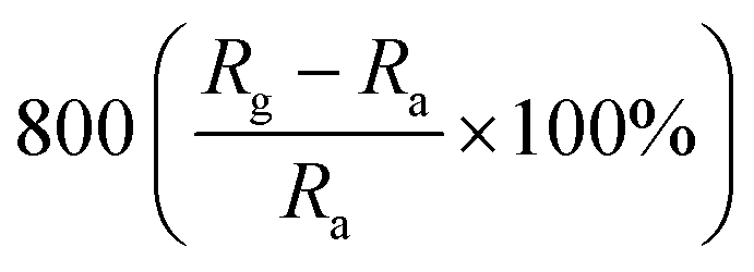 |
6.5/-min | 96 |
| Cr | Nanorods | 5 ppm | 100 °C |  |
— | 97 |
| W | Thin film | 10 ppm | 150 °C |  |
220/845 s | 98 |
| Polyaniline | Thin film | 20 ppm | RT |  |
2.16/2.83 min | 99 |
| Polyaniline | Nanorods | 100 ppm | RT |  |
83/399 s | 100 |
| Polypyrrole | Nanoparticles | 100 ppm | RT |  |
2–4 min/24 h | 101 |
| Poly(3-hexylthiophene) | Nanoparticles | 1 ppm | RT |  |
— | 102 |
Patil et al. deposited Cu-doped (1, 2, 3% volume percentage) ZnO (CZO) nanorods through a wet chemical route, and then annealed the samples.95 As shown in Fig. 5, the pure ZnO nanorods present a hexagonal shape at the top. As the Cu doping concentration increases, the diameter of the ZnO nanorods gradually increases and the length gradually decreases. In the sample CZO-3, the nanorods aggregate and become a broken rod state. This morphological change is due to the formation of the compound and the effective attraction of Cu ions to the ZnO (002) plane. The sample was used to detect NO2 gas. The results show that when the Cu concentration increases to 1%, the response value of Cu-doped ZnO to 1 ppm NO2 at 175 °C reaches a maximum value of 71. With the increases of doping concentration, the conductivity of ZnO changes from n-type to p-type, which is attributed to the generation of holes during the replacement of Zn sites by Cu atoms. It proved that the addition of an appropriate amount of Cu causes crystal defects in the ZnO nanorod, which helps to enhance the sensing performance of ZnO at low temperatures.
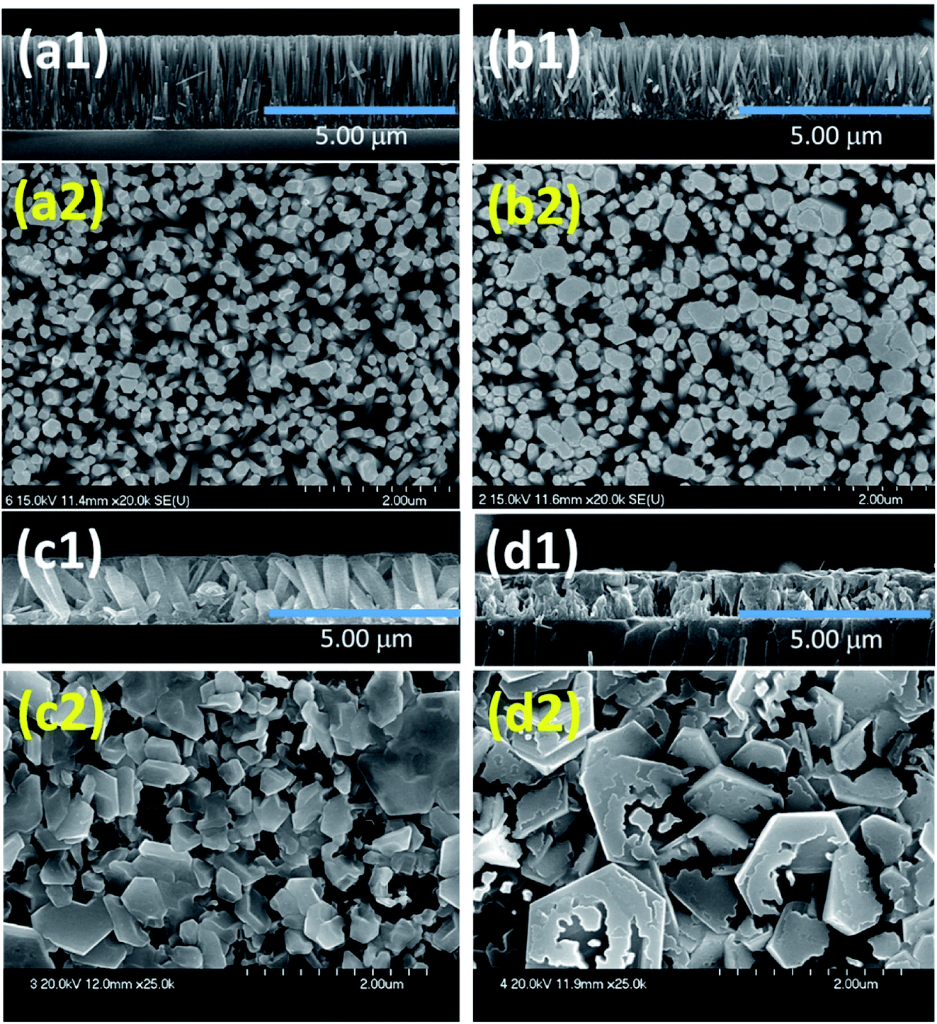 | ||
| Fig. 5 Surface and cross-sectional FESEM images of undoped and Cu doped ZnO thin films, (a) undoped ZnO, (b) CZO-1, (c) CZO-2 and (d) CZO-3. This figure has been reproduced with permission from ref. 90, Elsevier, Copyright 2017 (License Number: 4924050884483). This figure has been reproduced with permission from ref. 95, Elsevier, Copyright 2019 (License Number: 4924060417377). | ||
A facile hydrothermal route was followed by Chang et al. for developing films of Ce-doped ZnO nanorods array grown on the Al2O3 substrates with Pt spiral and interdigitated electrodes.96 Both the hydrothermal time and the content of Ce affect the gas-sensing response of the sensors. As shown in Fig. 6, the PL spectra show that the Ce-doped ZnO has a stronger green emission than the undoped ZnO at a concentration of 2 mM cerium nitrate, that is, the oxygen vacancies of Ce-doped ZnO increase, which is consistent with the XPS results. The results indicate that the Ce-doped ZnO nanorods with Ce precursor concentration of 2 mM and rod growth time of 2 h exhibit the highest response (800) towards 2 ppm NO2 and response time of 6.5 min. The sensor not only improves the response to NO2, but also reduces the operating temperature to 100 °C. Chang and co-workers also employed Cr-doped ZnO nanorods on Al2O3 substrate via hydrothermal route to monitor NO2 at 100 °C.97 It was found that Cr-doped ZnO nanorods (calcination temperature 400 °C, 0.1 mM Cr(NO3)3, rod growth time 4 h) exhibit good sensitivity, selectivity and response to NO2 gas. The lower operating temperature and the higher response of the Cr-doped ZnO nanorods sensor could be attributed to the high surface to volume ratio of the nanorods and larger active sensing area between spiral electrodes.
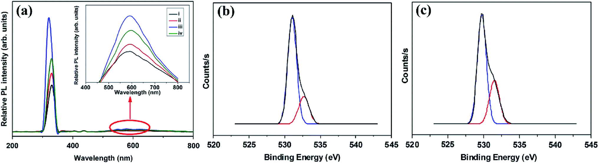 | ||
| Fig. 6 (a) PL spectra of (i) undoped and Ce-doped ZnO photocatalysts prepared with various Ce precursor concentrations: (ii) 1, (iii) 2, and (iv) 3 mM. The inset is the enlarged PL spectra within the visible light range. XPS O 1s spectra of (b) undoped ZnO and (c) Ce-doped ZnO nanorods with Ce precursor concentration of 2 mM and rod growth time of 2 h. This figure has been reproduced with permission from ref. 96, Elsevier, Copyright 2014 (License Number: 4924070322626). | ||
The response and recovery times of the sensor can be significantly shortened by the doping of metal ions into ZnO. For example, Tesfamichael et al. obtained W-doped ZnO thin films by depositing on glass and alumina substrates using magnetron sputtering.98 The W-doped ZnO thin film deposited at a pressure of 0.4 Pa using a lower sputtering power (30 W RF and 10 W DC) has high sensitivity (350) to NO2 and faster response time (220 s) and recover time (845 s) at a lower operating temperature (150 °C). Raman spectra show that doping W changes the properties of ZnO films and induces more free carrier defects. As a result, compared with the undoped ZnO film, the introduction of W doping increases the free carrier density in ZnO, so that the W doped ZnO film exhibits more significant low-temperature NO2 detection performance.
Sonker et al. reported that ZnO–PANI nanocomposite thin film sensor was used to detect NO2 at room temperature.99 They studied the effect of PANI concentration in the composite on NO2 gas-sensitivity. The ZnO–PANI (5%) sensor exhibits the most excellent gas-sensing performance for NO2, and its response value to 20 ppm NO2 is ∼6.11 × 10². They attribute the enhanced room-temperature sensing performance to the increase in electron transfer rate caused by the introduction of PANI (Fig. 7). Jain et al. prepared Ni doped ZnO/polyaniline (Ni:ZnO/PANI) nanocomposites using a wet chemical synthesis combined in situ oxidative polymerization technique.100 It was found that NO2 sensing performance of Ni:ZnO/PANI sensor has been significantly improved at room temperature. Both high response (75% to 100 ppm NO2) and fast response/recovery times (82/399 s) of Ni:ZnO/PANI sensor have been achieved. Apart from PANI, other conductive polymers also used to improve the sensing ability. Chougule et al. prepared the composite material of PPy and ZnO nanoparticles by spin coating.101 In this composite material, the weight ratios of ZnO are 10%, 20%, 30%, 40% and 50%, respectively. The results show that the composite containing ZnO (50%) has the best response to NO2. The maximum response value to 100 ppm NO2 at room temperature is 38%. It also has good selectivity and stability. Yang and co-workers manufactured P3HT with ZnO oxide-graphene oxide (ZnO@GO) hybrid for NO2 detection. They first used self-assembly methods to synthesize ZnO@GO composite.102 It is then spin-coated with P3HT on a silicon wafer to form organic field-effect transistors (OFETs). The P3HT with 60 wt% ZnO@GO composite sensor shows a high response to 5 ppm NO2 (210%). The doping of P3HT increases the conductivity.
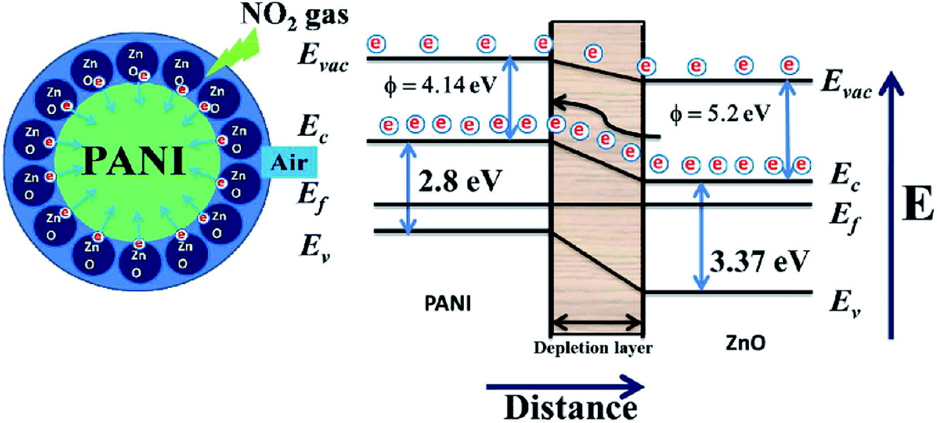 | ||
| Fig. 7 Schematic diagram of the proposed mechanism of NO2 sensing of ZnO/PANI heterojunctions. This figure has been reproduced with permission from ref. 99, RSC, Copyright 2016. | ||
3.4. Inorganic heterojunction sensitization
Using semiconductor oxides such as CuO, NiO, In2O3 and SnO2 in combination with ZnO also is an effective strategy to reduce the operating temperature of ZnO-based gas sensors. As well known, when two semiconductors are in contact with each other, the heterotype (p–n) or heterogeneous (n–n) heterojunctions will be formed according to the carrier conduction type, and the electrons will flow from the high Fermi level to the low side until the Fermi levels of the two materials have equilibrated.113,114 As a result, in this process, for the p–n heterojunctions, electrons accumulate on the low Fermi level and holes accumulate on the high Fermi level, forming a charge carrier depletion zone at the interface between the two materials. For the n–n heterojunctions, due to the loss of electrons, a depletion layer is formed on the surface of the semiconductor with a low Fermi level, which has a higher energy conduction band state. At the same time, due to the accumulation of electrons, an accumulation is formed on the surface of the semiconductor with a high Fermi energy level.52 For composite oxides with two different heterojunctions, on account of the difference in the original Fermi level of the material, a band bend occurs at the interface of the two materials to generate a barrier potential. Therefore, the potential barrier becomes an obstacle for charge carriers to pass through the interface, which is beneficial for gas sensing. In addition, the heterojunction can effectively accelerate the electron transfer between different particles, thereby shortening the response time of sensor. The following discusses some cases of using inorganic semiconductors to form heterojunctions for NO2 gas sensors.Xu et al. successfully prepared the brush-like (B-) SnO2@ZnO hierarchical nanostructures (HNSs) through a two-step hydrothermal method.115 The SnO2 nanowires (NWs) with a length of 1–1.5 μm and a diameter of ∼50 nm grow on the non-polar surface of the ZnO nanorods (NRs). The ZnO NRs with a length of 8–20 μm and a diameter of 0.5–1 μm are successfully packed tightly to form typical brush shape. As shown in Fig. 8, at 150 °C, the sensitivity of sensor to 1 ppm of NO2 is 25.5, which is significantly higher than the response of ZnO-based sensors and SnO2-based sensors to NO2. The minimum detection limit of B-SnO2@ZnO HNS for NO2 gas is 5 ppb, and the response/recovery times are less than 60 s. The enhancement of the inductive response is ascribed to the multi-junction between the brush-like SnO2 and ZnO, as shown in Fig. 9. Therefore, compared with pure ZnO and SnO2, the increase of multi-junctions (homojunction, heterojunction and Schottky barrier) in sensor based on B-SnO2@ZnO HNSs is the main factor that determines the excellent sensing performance of the sensor. Moreover, the barrier height greatly increased under NO2 exposure.
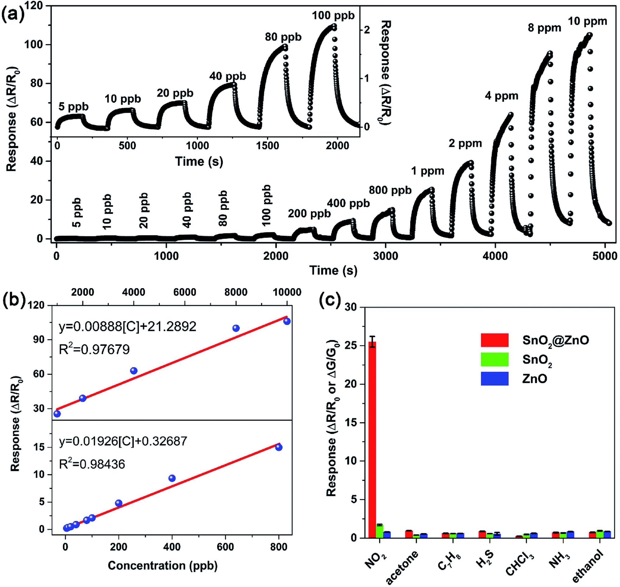 | ||
| Fig. 8 (a) Real-time response of the B-SnO2@ZnO HNSs sensor to NO2 from 5 ppb to 10 ppm. (b) The linear relationship of the B-SnO2@ZnO HNSs sensor to NO2 in the range of 5 ppb to 800 ppb and 1 ppm to 10 ppm. (c) Selectivity comparison of pristine ZnO, SnO2, and B-SnO2@ZnO HNSs sensors for different target gases at 1 ppm. This figure has been reproduced with permission from ref. 115, Elsevier, Copyright 2018 (License Number: 4924071319628). | ||
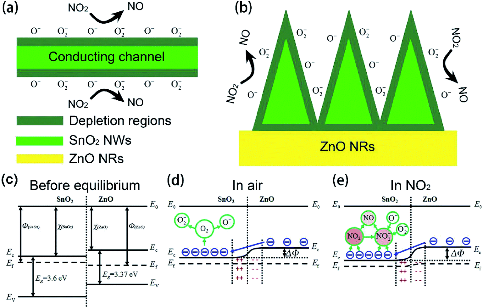 | ||
| Fig. 9 Schematic illustration of the sensing mechanisms. This figure has been reproduced with permission from ref. 115, Elsevier, Copyright 2018 (License Number: 4924071319628). | ||
Navale et al. reported a gas sensor based on the heterostructure of CuO nanoparticles-ZnO nanowires fabricated by thermal evaporation and annealing.116 The influence of annealing in different atmospheres on the sensor function was compared, the result is that the ZnO/CuO heterojunction sensor material annealed in argon atmosphere has the largest response to 100 ppm NO2 at 150 °C. This mechanism can be attributed to two key aspects. Firstly, the synergistic effects of CuO and ZnO help the dissociation of oxygen species at low temperatures; secondly, the heterojunction structure expands the electron depletion layer. A sensor based on ZnO nanorod/porous silicon nanowire (ZnO/PSiNW) hybrid structures exhibit a much higher response (35.1% to 50 ppm NO2) than those of ZnO nanorods and PSiNW working individually at room temperature.117 The selectivity of the sensor for NO2 sensing is excellent against the other gases including NO, methanol, methane. The article reveals that the p-type sensing behavior of the hybrids can be explained by the change in the energy band structure at the heterojunction of ZnO and PSiNWs when exposed to NO2. As a consequence, the significant increase in sensitivity is mainly ascribed to the faster transport of carriers in the hybrids, the increase in gas sensing area and the increase in oxygen vacancy concentration. Bai et al. successfully fabricated ZnO–SnO2 hollow nanofibers via a one-step electrospinning method and annealing treatment.118 The ZnO–SnO2 composite nanofibers consist of vast single phase particles and the surface area of SnZn20 (Zn atom percent of 20%) sample is calculated to be 36.83 m2 g−1. In addition, the HRTEM characterization indicates the existence of heterojunction at interface between the nanocrystal ZnO and SnO2. The SnZn20 sensor exhibits a high response with a value of 46 to 1 ppm NO2, which is 9 and 5.2 times higher than those made of pure ZnO and SnO2, respectively. The improvement in the sensing properties is attributed to the large specific surface area provided by hollow nanostructures and the formation of heterojunctions at interface between both metal oxides. Zhao et al. uniformly decorated In2O3 nanoparticles with a diameter of 3–5 nm on the surface of ZnO nanowires.119 The loading of ultra-fine In2O3 nanoparticles significantly improved the sensing performance of ZnO nanowires. Table 4 lists the complete reports of other structural studies based on ZnO nanostructures.
| Inorganic materials | Morphology (ZnO) | NO2 concentration | Temperature (°C) | Response | Response and recovery time | Ref. |
|---|---|---|---|---|---|---|
| SnO2 | Nanorods | 1 ppm | 150 °C | 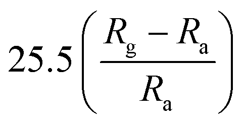 |
<60 s | 115 |
| CuO | Nanowires | 100 ppm | 150 °C |  |
14/197 s | 116 |
| In2O3 | Nanowires | 1 ppm | 150 °C | 54.6 (Rg/Ra) | 20/23 s | 119 |
| Silicon nanowire | Nanorods | 50 ppm | RT |  |
— | 117 |
| SnO2 | Nanofiber | 1 ppm | 90 °C | 46 (Rg/Ra) | 68/83 s | 118 |
3.5. Hybrid structures with 2D materials
2D nanostructured materials (graphene, transition metal dichalcogenides (TMDs), phosphorene, MXene) refer to materials with a single layer or several atomic layers, which exist in the form of nanosheets, nanofilms, and nanoflakes in structure.120 They have a large surface-to-volume ratio, more defects, vacancies and edge sites, so that they have higher adsorption efficiency and surface-active sites. Therefore, the composite materials that hybridize ZnO with 2D materials have proved to be a promising outstanding candidate in the field of gas-sensing. Due to ZnO and 2D materials have different work functions and semiconductor characteristics, heterojunctions are formed between the two materials.121 At the same time, when the 2D materials are doped in ZnO, it can improve the gas absorption and increase the selectivity of sensor. All of these factors contribute to the excellent sensing performance of ZnO/2D materials sensor for NO2 gas at low temperature.Among these 2D materials, the composite materials of reduced graphene oxide (rGO) and ZnO are the most studied gas-sensitive materials. An example of a composite material based on ZnO and rGO that responses to trace NO2 at low temperature was published by Qu's group.122 The wrapped ZnO/rGO nanocomposites were developed using a novel ultrasonic spray-assisted solvothermal (USS) method. Subsequently, various mass ratios of ZnO/rGO have been investigated. The sensor response of ZnO/rGO-0.5 is 62 for 50 ppm NO2 at 130 °C, which is 3 times higher than pure ZnO. Meantime, the detection limit of sensor is as low as 10 ppb, and it is also highly selective for NO2 gas. The promotion is attributed to the formation of Schottky junction and the porous structures. ZnO nanostructures with different morphologies have also been used in combination with rGO to prepare NO2 gas sensors. Xia et al. loaded ultrathin ZnO nanorods on rGO nanosheets via a facile two-step additive-free solution synthesis.123 For ZNR-3/rGO (the Zn2+/OH− ratio of the seed layer solution is 10), randomly oriented ZnO nanorods with an average diameter of 12 nm are densely distributed on the surface of rGO, forming a hedgehog-like nanocomposites with a high specific surface area (59.9 m2 g−1) and rich pore structure. Compared with the ZnO nanorods sensor and rGO sensor, the ultrathin ZnO nanorods/rGO mesoporous nanocomposites sensor reveals excellent response toward NO2 because rGO has the high transport capability and the composites with mesoporous structures has excellent NO2 adsorption ability. Liu and co-workers fabricated ZnO nanowalls decorated rGO nanosheets via a thermal reduction and soft solution process.124 The electrical properties of sample are tested, and the results show that the carrier concentration of the ZnO nanowalls/rGO heterojunction sensor is increased and the resistivity decrease. The sensor has good sensitivity to NO2 (9.61 to 50 ppm NO2) and fast response/recovery speed (25/15 s) at room temperature.
Furthermore, some strategies such as noble metals loading have also been applied to improve gas-sensitivity of ZnO/rGO composites. Liu et al. synthesized the ZnO–rGO–Au composites via depositing Au nanoparticles with a particle size of about 10–20 nm on the surface of the ZnO/rGO composite through a wet chemical route.125 The ZnO–rGO–Au composites sensor achieves high response, fast response and recovery, and high selectivity at lower operating temperature (80 °C). Many researchers have reported the gas-sensing characteristics of composites of ZnO and metal oxide combined with rGO. ZnO/SnO2 heterostructure on rGO constructed via combination of the hydrothermal method and the wet-chemical deposition method was reported.126 The sensor response (141.0%) of the composite to 5 ppm NO2 is 4 times and 3 times higher than that of SnO2–rGO (34.8%) and ZnO–rGO (43.3%) for 5 ppm NO2 at room temperature. A current versus voltage (I–V) study has been carried out, and the nonlinear rectification characteristics of ZnO/SnO2–rGO prove the existence of heterojunction between the hybrids. Thus, the enhanced sensing performance is attributed to the heterostructure between the nanomaterials, which makes the hybrids have excellent charge transfer capability, and improves the efficiency of interface charges transfer to adsorbed oxygen. Bai et al. reported a nanocomposite material that modified rGO on ZnO/CdO heterojunction by a one-step hydrothermal method.127 The results of a systematic comparison experiment show that the gas sensor made of ZnO/CdO/rGO (1.0 wt%) composite can operate at a low-working temperature and its performance is improved. This is attributed to the modulation of resistance by ZnO/CdO heterojunction and the modification of rGO with good conductivity. In addition, p–n heterojunctions are also formed at the interface between ZnO and rGO, and the charge transfer between them also enhances the adsorption of NO2 molecules (Fig. 10).
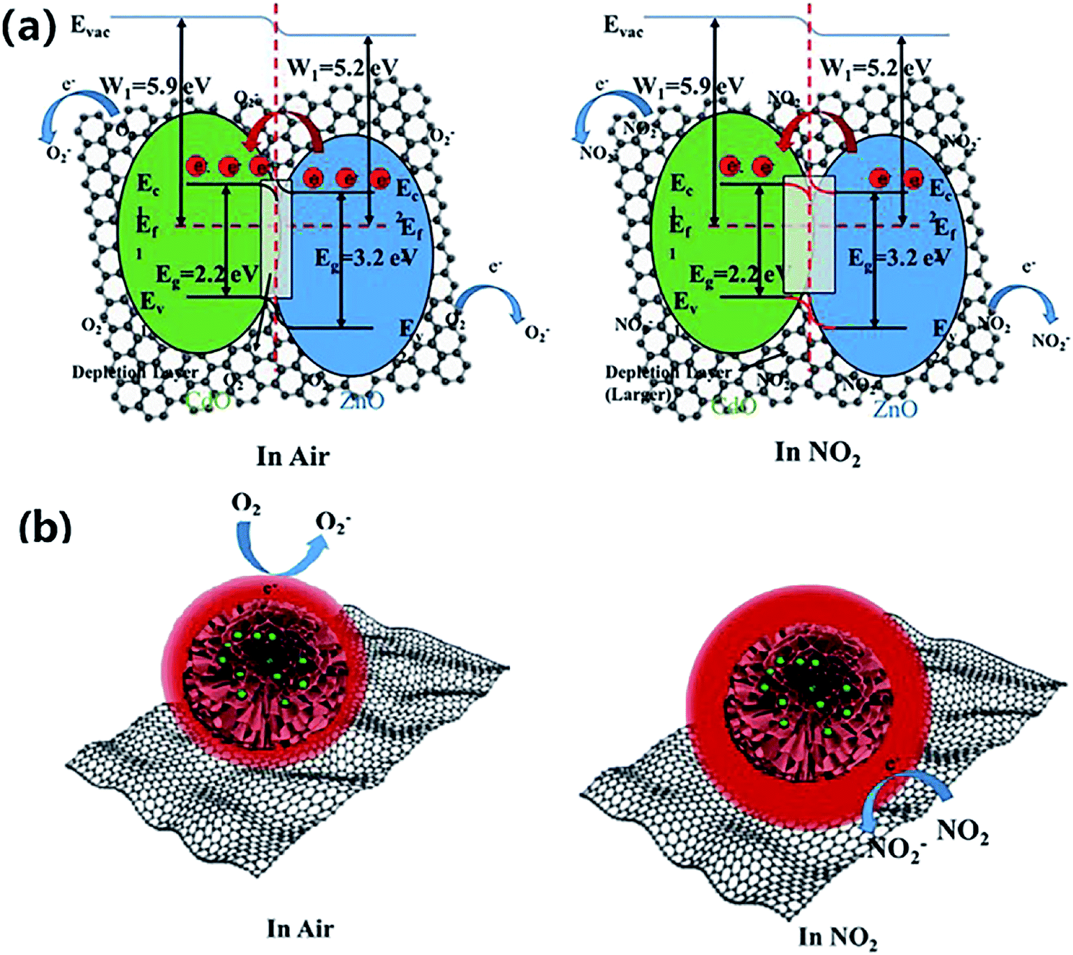 | ||
| Fig. 10 (a and b) Band diagram of hierarchical structure of gas adsorption and change of depletion layer for ZnO/CdO/rGO composite in air and NO2. This figure has been reproduced with permission from ref. 127, Elsevier, Copyright 2020 (License Number: 4924090847198). | ||
In addition, 2D MoS2 possess semiconductor properties, large surface area and atomic thin layer structure, which makes it suitable as a candidate material for gas adsorption and detection. Li et al. combined ZnO nanowires with MoS2 nanosheets at different mass ratios to test their NO2 sensing performance at low-operating temperatures.128 It has been found that the MoS2/ZnO sensor with a mass ratio of 1:2 has a high sensitivity (63%) to 50 ppb NO2 at 60 °C, with excellent repeatability and selectivity. On the one hand, the p–n-type heterojunction formed by MoS2 and ZnO modulates the width of the depletion layer. On the other hand, 2D MoS2 nanosheets and 1D ZnO nanowires are constructed as an unintegrated and porous structure, which is conducive to the process of molecular penetration and adsorption/desorption.
Black phosphorus (BP) has also proved to be a promising gas-sensing material due to its significant advantages over semi-metallic graphene, such as direct band gap related to thickness and high free carrier mobility. Therefore, combining BP with ZnO to prepare a novel gas-sensing material. Li et al. combined multi-layere BP nanosheets by ultrasonic treatment into ZnO hollow spheres obtained by microwave-assisted hydrothermal method.129 The sensor based on ZnO–BP composite material shows high response, fast response behavior, and the detection concentration of NO2 is as low as 1 ppb. The first-principle studies have confirmed that the gas-sensing mechanism of ZnO–BP is due to the excellent carrier mobility. Table 5 summarizes the low-temperature sensing characteristics of the composite of ZnO and 2D nanostructured materials.
| 2D materials | Morphology (ZnO) | NO2 concentration | Temperature (°C) | Response | Response and recovery time | Ref. |
|---|---|---|---|---|---|---|
| rGO | Nanoflowers | 2 ppm | 125 °C | 40 (Rg/Ra) | 43/50 s | 127 |
| MoS2 | Nanowires | 50 ppb | 60 °C |  |
— | 128 |
| rGO | Nanorods | 50 ppm | 130 °C | 62 (Rg/Ra) | 3/10 s | 122 |
| rGO | Nanorods | 1 ppm | RT |  |
75/132 s | 123 |
| rGO | Nanowalls | 50 ppm | RT | 9.61 (Rg/Ra) | 25/15 s | 124 |
| rGO | Nanoparticles | 100 ppm | 80 °C | 32.55  |
27/86 s | 125 |
| Black phosphorus | Hollow spheres | 100 ppb | 160 °C |  |
9/15 s | 129 |
| rGO | Nanoparticles | 5 ppm | RT |  |
33/92 s | 126 |
3.6. Light activation
Photon activation can replace thermal activation as a strategy for achieving room-temperature NO2 detection of ZnO-based gas sensors. Table 6 summarizes the room-temperature gas sensing performance of ZnO-based gas sensors under UV or visible light activation.| Light source | Material | NO2 concentration | Temperature (°C) | Response | Response and recovery time | Ref. |
|---|---|---|---|---|---|---|
| UV | ZnO | 1 ppm | RT | 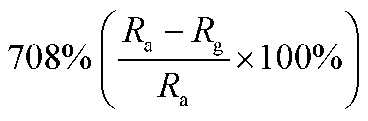 |
31/144 s | 130 |
| ZnO/SnO2 | 500 ppb | RT | 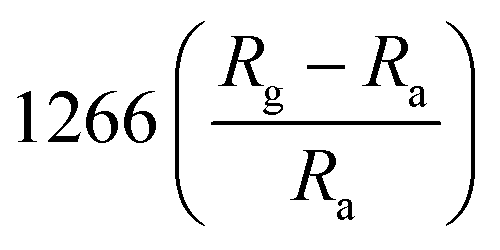 |
— | 131 | |
| ZnO/rGO | 50 ppm | RT | 35.31 (Rg/Ra) | 37/2 s | 132 | |
| ZnO | 1 ppm | RT | 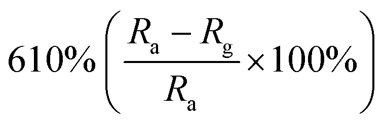 |
47/136 s | 133 | |
| ZnO/MoS2 | 200 ppb | RT | 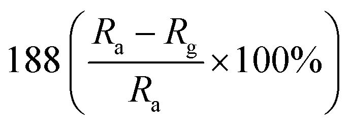 |
— | 134 | |
| ZnO | 50 ppb | RT |  |
— | 135 | |
| Visible light | ZnO/g-C3N4 | 7 ppm | RT | 44.8 (Rg/Ra) | 142/190 s | 136 |
| ZnO/Ag | 1 ppm | RT |  |
— | 137 | |
| ZnO/Au | 1 ppm | RT | 4.66 (Rg/Ra) | — | 138 | |
| ZnO/Pd | 100 ppb | RT |  |
25/29 s | 139 |
| hν → h+ + e−, RT | (9) |
| O2(gas) + e−(hν) → O2−(ads,hν), RT | (10) |
| NO2−(ads) + O2−(ads,hν) + e− → 2O−(ads) + NO2−(ads), RT | (11) |
Researchers have developed the ZnO-based NO2 gas sensors excited by UV illumination. Wang's group introduced surface oxygen vacancies (VO) by post-processing hydrothermally grown ZnO nanowires (NW) in NaBH4 solution.130 This approach combined the UV activation and surface (VO) engineering of ZnO nanostructures for achieving the NO2 detection at room temperature. Fig. 11a–c present the comparison of the dynamic response of sensors based on ZnO NW and VO–ZnO NW to NO2 gas under dark and UV illumination at room temperature. The results indicate that VO–ZnO NW with rich surface oxygen vacancies shows enhanced response and faster response recovery rate under UV illumination compared with ZnO NW. At the same time, the response of both samples under UV illumination to NO2 was significantly stronger than that under the dark. It can also be seen from Fig. 11d that the response of VO–ZnO NW increases from 267.3% to 708% with the increase intensity of UV illumination. The synergistic mechanism of UV activation and surface VO on the room-temperature gas sensing performance of ZnO NW can be schematically illustrated in Fig. 11e. UV illumination improves the photoelectric performance of ZnO, and the co-modulation of UV and VO promotes the adsorption and reaction of oxygen species and NO2, resulting in working at room temperature. Meantime, Wang et al. controlled the growth of ZnO nanosheet arrays with abundant nanojunctions on flexible substrates by using a water bath method.133 The SEM image reveals that the interconnected and vertically arranged nanosheets with a length/thickness of 200–500 nm and a thickness of 40–50 nm are uniformly grown on the substrate. The nitrogen adsorption analysis indicated a BET surface area of 56 m2 g−1 and a hollow structure. The gas-sensing tests of the sensor with two structures of nanosheets and nanorods show that the interconnected nanosheets improved NO2 sensing performance under the assistance of UV light due to the increased height of the interface potential barrier compared with nanorods. The sensitivity to 1000 ppb NO2 is 610% in ZnO nanosheets sensor. Wang and co-workers also synthesized polystyrene sulfonate (PSS) functionalized ZnO nanowires by hydrothermal method.135 Through this process, ZnO nanowires with lengths of 20–50 μm and diameters of 50–300 nm obtain high aspect ratio. The sensor shows a higher response (690% to 2 ppm NO2), a low detection limit (5 ppb), excellent reversibility and stability under UV light assist at room temperature. The I–V test shows that the surface-adsorbed PPS injects the electrons into ZnO nanowires by photo-assisted, which increases the light-induced carrier density, thereby increasing the number of electrons reacting with NO2 gas.
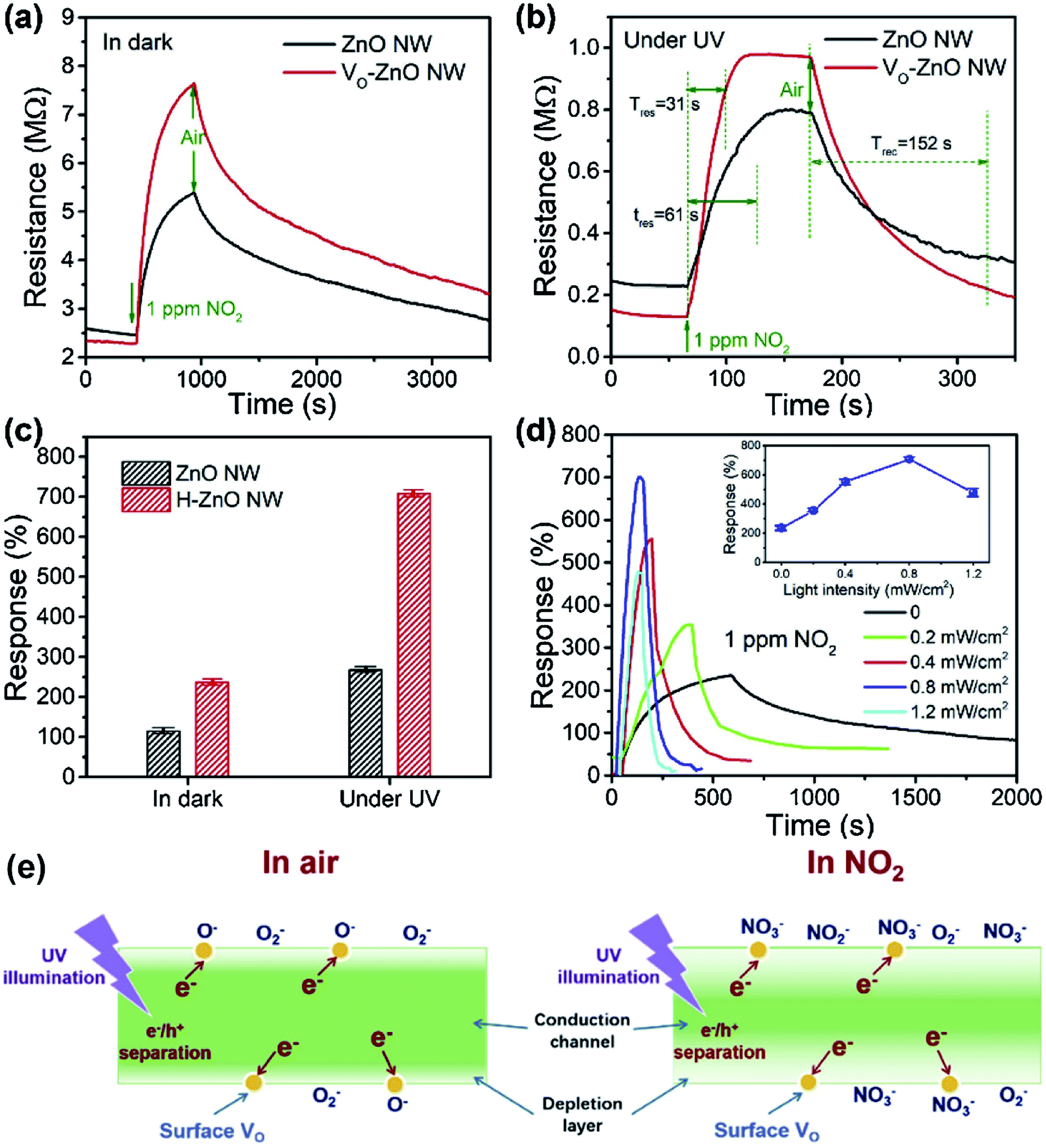 | ||
| Fig. 11 Dynamic resistance changes of the sensors based on ZnO NW and VO–ZnO NW to 1000 ppb of NO2 in dark (a) and under UV illumination (b) and (c) summarized sensing response of the sensors; (d) influence of light intensity on response curves and responses (inset) of the VO–ZnO NW-based sensor to 1000 ppb of NO2. (e) Schematic illustration of the mechanism for synergistic effects of UV activation and surface VO on the room-temperature NO2 gas sensing performance of ZnO nanowires. This figure has been reproduced with permission from ref. 130, Elsevier, Copyright 2019 (License Number: 4924100231565). | ||
According to the previous summaries, the heterojunctions in composite materials can observably improve the low-temperature NO2 gas-sensing performance. In fact, the existence of heterojunctions also inhibits the recombination of photo-generated charge carriers under UV light, thus the effective charge separation can increase the lifetime of charge carriers. Zhou et al. synthesized ZnO/SnO2 composite materials as a room-temperature and UV light-assisted NO2 gas sensor.131 The heterojunction formed at the contact between SnO2 nanoparticles and nanorods plays a vital role in expanding the depletion region. Fig. 12a and b investigated the gas sensing properties of different samples with and without UV illumination at room temperature. The results show the ZnO/SnO2 composite with Zn and Sn molar ratio of 1:1 (ZS3) exhibits a higher response to NO2 gas under UV light irradiation. Fig. 12c shows the enhancement mechanism of sensor to realize room-temperature detection under UV light. Qi et al. adopted spray, thermal reduction and simple solution methods to in situ grow ZnO nanowalls on porous rGO (PG) surface.132 As shown in Fig. 13a, a large number of micropores with a pore size range of 60–250 nm are distributed on the rough surface of the PG sheets. The Raman spectra display that PG has more defects. Fig. 13c shows the ZnO nanowalls touching each other at different inclination angles. The TEM image illustrates that the nanowalls grow vertically on the PG sheet and form heterojunctions. The gas-sensing test of ZnO/PG under UV radiation at room temperature shows that the hybrids have the highest response value of 35.31 and fast response/recovery speed (37/2 s) to 50 ppm NO2. This is because UV light radiation enhances the charge transfer efficiency, and the 3D hybrid structure provides many channels for gas diffusion. The UV-assisted NO2 gas sensor based on multilayer MoS2 nanosheet/ZnO nanowire composite material was reported by Zhou's group.134 The response of sensor to 200 ppb NO2 up to 188 under UV light irradiation, and has excellent repeatability and selectivity.
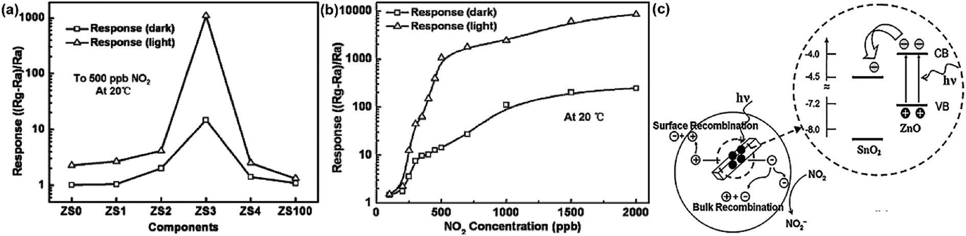 | ||
| Fig. 12 (a) Responses of the sensor based on the composite materials with the various molar ratio of ZnO to SnO2 to 500 ppb NO2 at room temperature with and without UV light irradiation. (b) Response of the ZS3 sensor vs. NO2 concentration at room temperature with and without UV light irradiation. (c) Schematic diagram: the carriers transport with UV light stimulated, energy band structure and electron–hole pair separation in the ZnO/SnO2 heterostructure in the area marked with a dashed circle. This figure has been reproduced with permission from ref. 131, Elsevier, Copyright 2012 (License Number: 4924100838478). | ||
 | ||
| Fig. 13 (a) The SEM image of PG (b) the Raman spectra of PG (c) the SEM image and the inset of EDS of ZnO/PG hybrids (d) TEM image of ZnO/rGO hybrids. This figure has been reproduced with permission from ref. 132, Elsevier, Copyright 2018 (License Number: 4924110156230). | ||
Wang et al. prepared ZnO/g-C3N4 composite material by ultrasonic mixing and calcination process.136 As shown in Fig. 14a, the absorption range of visible light of the composite material is determined by UV-vis measurement, and excitation source of different wavelengths are selected. Fig. 14b–f compare the gas-sensing performance of ZnO loaded with different wt% (0, 5, 10, 15 wt%) of g-C3N4 to NO2 under UV light and visible light of different wavelengths. Under the light excitation of 460 nm, ZnO/g-C3N4 10 wt% shows the most excellent gas-sensing properties at room temperature, its response value to 7 ppm NO2 reached a maximum of 44.8, and the detection limit was 38 ppb. They successfully proved that the wavelength of visible light has a significant influence on the sensing ability of ZnO/g-C3N4. The realization of the room temperature detection and the improvement of the response ability are attributed to the absorption rate of g-C3N4 in the visible region and the charge separation at the interface of the composite material.
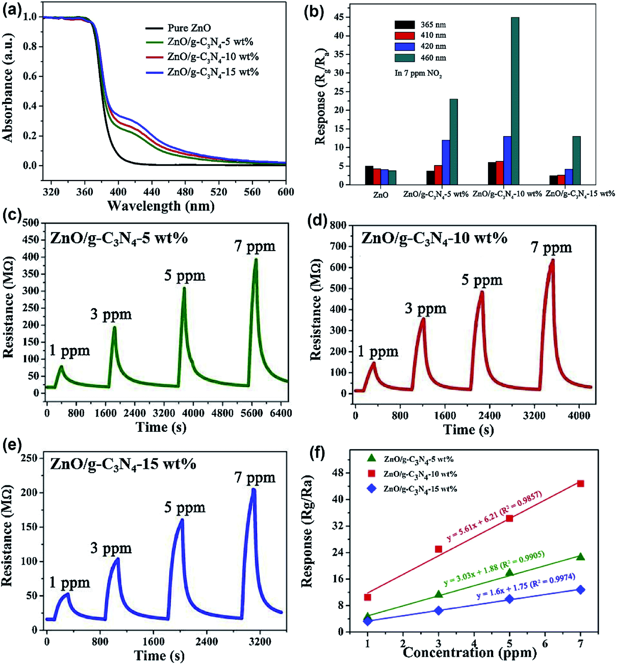 | ||
| Fig. 14 (a) UV-vis spectra of pure ZnO and ZnO/g-C3N4 composites. (b) The responses of as-prepared samples to 7 ppm NO2 under different wavelength light illumination. (c–e) The dynamic resistance curves of ZnO/g-C3N4-5 wt%, ZnO/g-C3N4-10 wt%, and ZnO/g-C3N4-15 wt% to different concentrations of NO2 under 460 nm light illumination, respectively; (f) linearity of response curves of ZnO/g-C3N4 composites. This figure has been reproduced with permission from ref. 136, Elsevier, Copyright 2020 (License Number: 4924111472674). | ||
Since metal nanoparticles have enhanced light absorption capacity, metal nanoparticles on the surface of ZnO will use the resonant plasmonic effect to improve the optoelectronic and gas sensing performance. Zhang's group reported that ZnO–Ag nanoparticle synthesized by the polymer-network gel method used for room temperature NO2 detection under visible light.137 They found that the key factor to improve the light-assisted room-temperature sensing performance of NO2 is to adjust the appropriate number of surface area electrons by optimizing the working wavelength.
In addition, the synergistic effects between Ag NPs modification and oxygen vacancies also inhibit electron–hole recombination and improves the efficiency of gas-sensing. Wang et al. synthesized ultra-thin ZnO nanorods by a nanoseed-assisted wet chemical method, and then loaded Au nanoparticles on the surface of nanorods by a photoreduction method.138 The sensor successfully attempted to control the gas selectivity with light, achieving higher selectivity to NH3 in the dark, and higher selectivity to NO2 under visible light at room temperature. In addition, the sensor shows high response (4.66 towards 1 ppm NO2) and reversibility to NO2 under visible light at room temperature. This is due to the surface plasmon resonance effect of Au nanoparticles that induces the visible light modulation of the surface depletion characteristics of ZnO, the optical property is proved by UV-vis diffuse reflectance spectroscopy. Wang et al. also prepared ZnO/Pd hybrid materials to achieve a high response of ppb level NO2 under visible light at room temperature.139 In the end, we provide a table referring to the abbreviations in the text and their corresponding full names (Table 7).
| Abbreviation | Full name |
|---|---|
| NO2 | Nitrogen dioxide |
| MOSs | Metal oxide semiconductors |
| PL | Photoluminescence |
| SEM | Scanning electron microscope |
| XPS | X-ray photoelectron spectroscopy |
| HRTEM | High-resolution transmission electron microscopy |
| VOCs | Volatile organic compounds |
| FESEM | Field emission scanning electron microscope |
| PPy | Polypyrrole |
| P3HT | Poly(3-hexylthiophene) |
| PANI | Polyaniline |
| OFETs | Organic field-effect transistors |
| 1D | One-dimensional |
| 2D | Two-dimensional |
| TMDs | Transition metal dichalcogenides |
| rGO | Reduced graphene oxide |
| USS | Ultrasonic spray-assisted solvothermal |
| I–V | Current versus voltage |
| BP | Black phosphorus |
| PSS | Polystyrene sulfonate |
4. Conclusions and future outlook
In general, ZnO has the advantages of wide band gap, high conductivity electron mobility, stable physical and chemical properties, easy preparation, and can be adjusted to various morphological, which undoubtedly proves that ZnO has the potential to prepare gas-sensitive materials. Nevertheless, the realization of ZnO-based gas sensors to monitor NO2 at low temperatures is still a challenge. Therefore, the operation of ZnO-based gas sensors at low temperatures has stimulated tremendous research potential, and many efforts have been reviewed and analyzed in the following:(1) The surface morphology and structure of ZnO nanomaterials can be adjusted, such as ZnO nanoparticles, nanorods, nanotubes, nanofibers, nanosheets, nanoflowers, as a consequence of controlling the grain size to increase the effective ratio surface area, defect density and porosity, thereby providing more active sites for gas reactions. Additionally, for n-type semiconductor ZnO, the donor defect level is dominant. Surface defects have a significant impact on the sensing properties of ZnO, which increases the number of oxygen adsorption sites on the surface of ZnO, thereby improving the efficiency of the redox reaction.53
(2) With the mechanism of electronic sensitization and chemical sensitization, the operating temperatures of sensors are reduced and the sensitivity and other sensing parameters are improved through the noble metal functionalized ZnO. The key point of this method is to effectively control the size and distribution of noble metal nanoparticles.
(3) It is believed that doping additives in ZnO will increase the active sites and defects on the surface of ZnO, thereby contributing to the adsorption and desorption of NO2.
(4) Regarding compounding with other nanomaterials, the heterojunctions with ZnO is used to modulate the resistance changes of the sensing material before and after exposure to NO2 to improve the gas-sensing characteristics. At the same time, the formation of heterojunctions also speeds up the transfer of electrons between different materials and accelerates the response speed of sensors.
(5) Finally, photoactivation is to replace the heat source with a light source to provide energy for the operation of sensor, which can also reduce the operating temperature of sensors.
However, it must be said that compounding with other nanomaterials and using light sources to illuminate increase the cost of sensor. The research of sensors will develop towards low energy consumption, integration and small size. Meanwhile, many challenges and problems focus on improving sensitivity, shortening response and recovery times, achieving selectivity, repeatability, and long-term stability at room temperature:
(1) First of all, the different humidity conditions will interfere with the sensing characteristics of ZnO-based gas sensors. In particular, high humidity conditions will seriously affect the response and recovery speed of sensors. In general, the results of gas-sensitivity tests in the literature are conducted in a well-controlled laboratory environment. However, in practical applications, the humidity changes with the environment. Therefore, the room-temperature gas-sensitivity performance under different humidity conditions should be systematically studied to correct the sensing results.
(2) The control of material morphology is an important part of the process to achieve room-temperature detection of NO2. The surface engineering design of ZnO affects the exposed high-energy surfaces, surface defects and active sites to some extent. Therefore, the optimization of micro-topography should be used to guide the manufacture of better gas sensors.
(3) In addition, integrating the sensing materials directly on the electrodes not only simplifies the fabrication process of gas sensors. It also avoids the destruction of the morphology when the nanomaterials are screen-printed, used with adhesives or applied to the electrodes. The vertically-oriented ZnO grown in situ directly on substrates/electrodes has a high specific surface area and an efficient carrier transport channel, which significantly improves the gas-sensing performance of ZnO and promotes its application in actual room-temperature detection.
(4) Finally, there is also a desire to develop flexible wearable gas sensors for applications in daily life. However, problems are prone to occur in device manufacturing, such as cracking and shedding of materials. Thus, this problem needs to be corrected in order to achieve a reliable room-temperature flexible gas sensor.
These challenges should be overcome to extend laboratory-scale academic research on ZnO-based NO2 gas sensors to practical applications. We hope that our review will inspire the further development of ZnO-based sensing materials in gas sensor applications and make them perform well in the future.
Conflicts of interest
There are no conflicts to declare.Acknowledgements
This work was supported financially by National Natural Science Foundation of China (No. 11904209, 61904098), Natural Science Foundation of Shandong Province (No. ZR2019QF018) and Higher Education Research and Development Program of Shandong Province (No. J18KA242).References
- X. Chen, Y. Shen, W. Zhang, J. Zhang, D. Wei, R. Lu, L. Zhu, H. Li and Y. Shen, Appl. Surf. Sci., 2018, 435, 1096–1104 CrossRef CAS.
- R. Chen, J. Wang, Y. Xia and L. Xiang, Sens. Actuators, B, 2018, 255, 2538–2545 CrossRef CAS.
- Y. Y. Broza, X. Zhou, M. Yuan, D. Qu, Y. Zheng, R. Vishinkin, M. Khatib, W. Wu and H. Haick, Chem. Rev., 2019, 119, 11761–11817 CrossRef CAS.
- Ü. Özgür, Y. I. Alivov, C. Liu, A. Teke, M. A. Reshchikov, S. Doğan, S.-J. Cho and H. Morkoç, J. Appl. Phys., 2005, 98, 041301 CrossRef.
- Y. Li, S. Wang, P. Hao, J. Tian, H. Cui and X. Wang, Sens. Actuators, B, 2018, 273, 751–759 CrossRef CAS.
- S. Agarwal, P. Rai, E. N. Gatell, E. Llobet, F. Güell, M. Kumar and K. Awasthi, Sens. Actuators, B, 2019, 292, 24–31 CrossRef CAS.
- J.-Y. Kim, J.-H. Lee, J.-H. Kim, A. Mirzaei, H. Woo Kim and S. S. Kim, Sens. Actuators, B, 2019, 299, 126965 CrossRef CAS.
- Z. Li, Y. Liu, D. Guo, J. Guo and Y. Su, Sens. Actuators, B, 2018, 271, 306–310 CrossRef CAS.
- D. Li, X. Zu, D. Ao, Q. Tang, Y. Fu, Y. Guo, K. Bilawal, M. B. Faheem, L. Li, S. Li and Y. Tang, Sens. Actuators, B, 2019, 294, 55–61 CrossRef CAS.
- N. S. A. Eom, H.-B. Cho, H.-R. Lim, B. S. Kim and Y.-H. Choa, Sens. Actuators, B, 2019, 300, 127009 CrossRef CAS.
- M. Tonezzer, J.-H. Kim, J.-H. Lee, S. Iannotta and S. S. Kim, Sens. Actuators, B, 2019, 281, 670–678 CrossRef CAS.
- W. Du, N. Wu, Z. Wang, J. Liu, D. Xu and W. Liu, Sens. Actuators, B, 2018, 257, 427–435 CrossRef CAS.
- A. Monamary, K. Vijayalakshmi and S. D. Jereil, Sens. Actuators, B, 2019, 287, 278–289 CrossRef CAS.
- P.-G. Su, F.-Y. Chen and C.-H. Wei, Sens. Actuators, B, 2018, 254, 1125–1132 CrossRef CAS.
- G. Zhao, J. Xuan, Q. Gong, L. Wang, J. Ren, M. Sun, F. Jia, G. Yin and B. Liu, ACS Appl. Mater. Interfaces, 2020, 12, 8573–8582 CrossRef CAS.
- X. Song, Q. Xu, T. Zhang, B. Song, C. Li and B. Cao, Sens. Actuators, B, 2018, 268, 170–181 CrossRef CAS.
- L. Guo, N. Xie, C. Wang, X. Kou, M. Ding, H. Zhang, Y. Sun, H. Song, Y. Wang and G. Lu, Sens. Actuators, B, 2018, 255, 1015–1023 CrossRef CAS.
- S. Li, Y. Diao, Z. Yang, J. He, J. Wang, C. Liu, F. Liu, H. Lu, X. Yan, P. Sun and G. Lu, Sens. Actuators, B, 2018, 276, 526–533 CrossRef CAS.
- J. Cao, H. Dou, H. Zhang, H. Mei, S. Liu and T. Zhang, Sens. Actuators, B, 2014, 198, 180–187 CrossRef CAS.
- Y. Gui, K. Tian, J. Liu, L. Yang, H. Zhang and Y. Wang, J. Hazard. Mater., 2019, 380, 120876 CrossRef CAS.
- S. Li, A. Liu, Z. Yang, L. Zhao, J. Wang, F. Liu, R. You, J. He, C. Wang, X. Yan, P. Sun, X. Liang and G. Lu, Sens. Actuators, B, 2019, 289, 252–259 CrossRef CAS.
- J. Jeevanandam, A. Barhoum, Y. S. Chan, A. Dufresne and M. K. Danquah, Beilstein J. Nanotechnol., 2018, 9, 1050–1074 CrossRef CAS.
- S. Singkammo, A. Wisitsoraat, C. Sriprachuabwong, A. Tuantranont, S. Phanichphant and C. Liewhiran, ACS Appl. Mater. Interfaces, 2015, 7, 3077–3092 CrossRef CAS.
- K. Suematsu, Y. Shin, Z. Hua, K. Yoshida, M. Yuasa, T. Kida and K. Shimanoe, ACS Appl. Mater. Interfaces, 2014, 6, 5319–5326 CrossRef CAS.
- S. Jana and A. Mondal, ACS Appl. Mater. Interfaces, 2014, 6, 15832–15840 CrossRef CAS.
- J. Huang, Y. Zhu, H. Zhong, X. Yang and C. Li, ACS Appl. Mater. Interfaces, 2014, 6, 7055–7062 CrossRef CAS.
- N. Banerjee and S. Roy, EDCT, 2018 Search PubMed.
- A. Dey, S. Roy and S. K. Sarkar, J. Mater. Eng. Perform., 2018, 27, 2701–2707 CrossRef CAS.
- K. B. D. B. Punzalan, F. K. B. Manalo and E. A. Florido, Key Eng. Mater., 2018, 775, 266–271 Search PubMed.
- S. Kumar, V. Pavelyev, P. Mishra, N. Tripathi, P. Sharma and F. Calle, Mater. Sci. Semicond. Process., 2020, 107, 104865 CrossRef CAS.
- T. Wu, Z. Wang, M. Tian, J. Miao, H. Zhang and J. Sun, Sens. Actuators, B, 2018, 259, 526–531 CrossRef CAS.
- T. Pauporté, O. Lupan, V. Postica, M. Hoppe, L. Chow and R. Adelung, Phys. Status Solidi A, 2018, 215, 1700824 CrossRef.
- L. Zhu, W. Zeng and Y. Li, Mater. Lett., 2018, 228, 331–333 CrossRef CAS.
- V. L. Patil, S. A. Vanalakar, A. S. Kamble, S. S. Shendage, J. H. Kim and P. S. Patil, RSC Adv., 2016, 6, 90916–90922 RSC.
- S. Bai, J. Hu, D. Li, R. Luo, A. Chen and C. C. Liu, J. Mater. Chem., 2011, 21, 12288 RSC.
- K.-S. Choi and S.-P. Chang, Mater. Lett., 2018, 230, 48–52 CrossRef CAS.
- K. Shingange, H. C. Swart and G. H. Mhlongo, Phys. B, 2018, 535, 216–220 CrossRef CAS.
- F. Cao, C. Li, M. Li, H. Li, X. Huang and B. Yang, Appl. Surf. Sci., 2018, 447, 173–181 CrossRef CAS.
- W. Zang, Y. Nie, D. Zhu, P. Deng, L. Xing and X. Xue, J. Phys. Chem. C, 2014, 118, 9209–9216 CrossRef CAS.
- A. R. Muchtar, N. L. W. Septiani, M. Iqbal, A. Nuruddin and B. Yuliarto, J. Electron. Mater., 2018, 47, 3647–3656 CrossRef CAS.
- E. Espid and F. Taghipour, ECS J. Solid State Sci. Technol., 2018, 7, Q3089–Q3093 CrossRef CAS.
- R. Ahmad, S. M. Majhi, X. Zhang, T. M. Swager and K. N. Salama, Adv. Colloid Interface Sci., 2019, 270, 1–27 CrossRef CAS.
- P. Patil, G. Gaikwad, D. R. Patil and J. Naik, Bull. Mater. Sci., 2016, 39, 655–665 CrossRef CAS.
- J. Xu, Y. Shun, Q. Pan and J. Qin, Sens. Actuators, B, 2000, 66, 161–163 CrossRef CAS.
- L. Zhu and W. Zeng, Mater. Lett., 2017, 209, 244–246 CrossRef CAS.
- G. Zhao, J. Xuan, X. Liu, F. Jia, Y. Sun, M. Sun, G. Yin and B. Liu, Nanomaterials, 2019, 9, 435 CrossRef CAS.
- R. Kumar, X. Liu, J. Zhang and M. Kumar, Nano-Micro Lett., 2020, 12, 164 CrossRef.
- Z. Li, H. Li, Z. Wu, M. Wang, J. Luo, H. Torun, P. Hu, C. Yang, M. Grundmann, X. Liu and Y. Fu, Mater. Horiz., 2019, 6, 470–506 RSC.
- Z. Jing and J. Zhan, Adv. Mater., 2008, 20, 4547–4551 CrossRef CAS.
- A. Wei, L. Pan and W. Huang, Mater. Sci. Eng., B, 2011, 176, 1409–1421 CrossRef CAS.
- L. Zhu and W. Zeng, Sens. Actuators, A, 2017, 267, 242–261 CrossRef CAS.
- C. Zhang, Y. Luo, J. Xu and M. Debliquy, Sens. Actuators, A, 2019, 289, 118–133 CrossRef CAS.
- P. Srinivasan, M. Ezhilan, A. J. Kulandaisamy, K. J. Babu and J. B. B. Rayappan, J. Mater. Sci.: Mater. Electron., 2019, 30, 15825–15847 CrossRef CAS.
- A. Mirzaei, J.-H. Kim, H. W. Kim and S. S. Kim, J. Mater. Chem. C, 2018, 6, 4342–4370 RSC.
- A. Mirzaei, J.-H. Kim, H. W. Kim and S. S. Kim, Sens. Actuators, B, 2018, 258, 270–294 CrossRef CAS.
- A. Mirzaei, S. G. Leonardi and G. Neri, Ceram. Int., 2016, 42, 15119–15141 CrossRef CAS.
- N. H. Al-Hardan, A. A. Aziz, M. J. Abdullah and N. M. Ahmed, ECS J. Solid State Sci. Technol., 2018, 7, P487–P490 CrossRef CAS.
- J. Ding, S. Chen, N. Han, Y. Shi, P. Hu, H. Li and J. Wang, Ceram. Int., 2020, 46, 15152–15158 CrossRef CAS.
- C. Xiao, T. Yang, M. Chuai, B. Xiao and M. Zhang, Phys. Chem. Chem. Phys., 2016, 18, 325–330 RSC.
- M. S. Choi, H. G. Na, A. Mirzaei, J. H. Bang, W. Oum, S. Han, S.-W. Choi, M. Kim, C. Jin, S. S. Kim and H. W. Kim, J. Alloys Compd., 2019, 811, 151975 CrossRef CAS.
- L. Parellada-Monreal, I. Castro-Hurtado, M. Martínez-Calderón, L. Presmanes and G. G. Mandayo, Appl. Surf. Sci., 2019, 476, 569–575 CrossRef CAS.
- Y. F. Sun, S. B. Liu, F. L. Meng, J. Y. Liu, Z. Jin, L. T. Kong and J. H. Liu, Sensors, 2012, 12, 2610–2631 CrossRef CAS.
- B. Min and S.-D. Choi, Sens. Actuators, B, 2004, 98, 239–246 CrossRef CAS.
- M. Al-Hashem, S. Akbar and P. Morris, Sens. Actuators, B, 2019, 301, 126845 CrossRef CAS.
- P. G. Choi, T. Fuchigami, K. I. Kakimoto and Y. Masuda, ACS Sens., 2020, 5, 1665–1673 CrossRef CAS.
- Y. Xu, L. Zheng, C. Yang, W. Zheng, X. Liu and J. Zhang, ACS Appl. Mater. Interfaces, 2020, 12, 20704–20713 CrossRef CAS.
- N. J. Ridha, F. K. M. Alosfur, M. H. H. Jumali and S. Radiman, J. Phys. D: Appl. Phys., 2018, 51, 435101 CrossRef.
- O. Lupan, V. Postica, R. Adelung, F. Labat, I. Ciofini, U. Schürmann, L. Kienle, L. Chow, B. Viana and T. Pauporté, Phys. Status Solidi RRL, 2018, 12, 1700321 CrossRef.
- D. V. Ponnuvelu, S. Abdulla and B. Pullithadathil, ChemistrySelect, 2018, 3, 7156–7163 CrossRef CAS.
- Y. Zhu, Y. Wang, G. Duan, H. Zhang, Y. Li, G. Liu, L. Xu and W. Cai, Sens. Actuators, B, 2015, 221, 350–356 CrossRef CAS.
- F. Meng, S. Ge, Y. Jia, B. Sun, Y. Sun, C. Wang, H. Wu, Z. Jin and M. Li, J. Alloys Compd., 2015, 632, 645–650 CrossRef CAS.
- Y. Xia, J. Wang, X. Li, X. Dan, D. Zhou, L. Xiang and S. Komarneni, Ceram. Int., 2016, 42, 15876–15880 CrossRef CAS.
- D. Yan, M. Hu, S. Li, J. Liang, Y. Wu and S. Ma, Electrochim. Acta, 2014, 115, 297–305 CrossRef CAS.
- R. Chen, J. Wang and L. Xiang, Sens. Actuators, B, 2018, 270, 207–215 CrossRef CAS.
- Y. Xia, L. Zhou, J. Yang, P. Du, L. Xu and J. Wang, ACS Appl. Electron. Mater., 2020, 2, 580–589 CrossRef CAS.
- L. Yu, F. Guo, S. Liu, B. Yang, Y. Jiang, L. Qi and X. Fan, J. Alloys Compd., 2016, 682, 352–356 CrossRef CAS.
- M. Chen, Z. Wang, D. Han, F. Gu and G. Guo, J. Phys. Chem. C, 2011, 115, 12763–12773 CrossRef CAS.
- J.-H. Kim, A. Mirzaei, H. W. Kim and S. S. Kim, Sens. Actuators, B, 2018, 267, 597–607 CrossRef CAS.
- H. Tian, H. Fan, J. Ma, Z. Liu, L. Ma, S. Lei, J. Fang and C. Long, J. Hazard. Mater., 2018, 341, 102–111 CrossRef.
- H. Kim, Y. Pak, Y. Jeong, W. Kim, J. Kim and G. Y. Jung, Sens. Actuators, B, 2018, 262, 460–468 CrossRef CAS.
- Z. Yin, X. Wang, F. Sun, X. Tong, C. Zhu, Q. Lv, D. Ye, S. Wang, W. Luo and Y. Huang, Sci. Rep., 2017, 7, 12206 CrossRef.
- A. Dey, Mater. Sci. Eng., B, 2018, 229, 206–217 CrossRef CAS.
- M. S. Barbosa, P. H. Suman, J. J. Kim, H. L. Tuller, J. A. Varela and M. O. Orlandi, Sens. Actuators, B, 2017, 239, 253–261 CrossRef CAS.
- U. T. Nakate, R. N. Bulakhe, C. D. Lokhande and S. N. Kale, Appl. Surf. Sci., 2016, 371, 224–230 CrossRef CAS.
- J.-H. Kim, A. Mirzaei, H. W. Kim and S. S. Kim, Sens. Actuators, B, 2019, 285, 358–367 CrossRef CAS.
- Y. Wang, B. Zhang, J. Liu, Q. Yang, X. Cui, Y. Gao, X. Chuai, F. Liu, P. Sun, X. Liang, Y. Sun and G. Lu, Sens. Actuators, B, 2016, 236, 67–76 CrossRef CAS.
- S. Zhang, P. Song, J. Zhang, H. Yan, J. Li, Z. Yang and Q. Wang, Sens. Actuators, B, 2017, 242, 983–993 CrossRef CAS.
- A.-G. Boudjahem and M. M. Bettahar, J. Mol. Catal. A: Chem., 2016, 426, 190–197 CrossRef.
- A. Lueking and R. T. Yang, J. Catal., 2002, 206, 165–168 CrossRef CAS.
- F. E. Annanouch, Z. Haddi, M. Ling, F. di Maggio, S. Vallejos, T. T. Vilic, T. Shujah, P. Umek, C. Bittencourt, C. S. Blackman and E. Llobet, ACS Appl. Mater. Interfaces, 2016, 8, 10413–10421 CrossRef CAS.
- X. Chen, Y. Shen, P. Zhou, S. Zhao, X. Zhong, G. Li, C. Han, D. Wei and D. Meng, Sens. Actuators, B, 2019, 280, 151–161 CrossRef CAS.
- X. Chen, Y. Shen, P. Zhou, X. Zhong, G. Li, C. Han, D. Wei and S. Li, Sens. Actuators, B, 2019, 289, 160–168 CrossRef CAS.
- V. P. Dinesh, A. Sukhananazerin and P. Biji, J. Alloys Compd., 2017, 712, 811–821 CrossRef CAS.
- G. Namgung, Q. T. H. Ta, W. Yang and J. S. Noh, ACS Appl. Mater. Interfaces, 2019, 11, 1411–1419 CrossRef CAS.
- V. L. Patil, S. A. Vanalakar, N. L. Tarwal, A. P. Patil, T. D. Dongale, J. H. Kim and P. S. Patil, Sens. Actuators, A, 2019, 299, 111611 CrossRef CAS.
- C.-J. Chang, C.-Y. Lin, J.-K. Chen and M.-H. Hsu, Ceram. Int., 2014, 40, 10867–10875 CrossRef CAS.
- C.-J. Chang, J.-K. Chen and T.-L. Yang, J. Taiwan Inst. Chem. Eng., 2014, 45, 1876–1882 CrossRef CAS.
- T. Tesfamichael, C. Cetin, C. Piloto, M. Arita and J. Bell, Appl. Surf. Sci., 2015, 357, 728–734 CrossRef CAS.
- R. K. Sonker, B. C. Yadav, A. Sharma, M. Tomar and V. Gupta, RSC Adv., 2016, 6, 56149–56158 RSC.
- S. Jain, N. Karmakar, A. Shah and N. G. Shimpi, Mater. Sci. Eng., B, 2019, 247, 114381 CrossRef CAS.
- M. A. Chougule, D. S. Dalavi, S. Mali, P. S. Patil, A. V. Moholkar, G. L. Agawane, J. H. Kim, S. Sen and V. B. Patil, Measurement, 2012, 45, 1989–1996 CrossRef.
- Y. Yang and H. E. Katz, J. Mater. Chem. C, 2017, 5, 2160–2166 RSC.
- V. S. Bhati, S. Ranwa, M. Fanetti, M. Valant and M. Kumar, Sens. Actuators, B, 2018, 255, 588–597 CrossRef CAS.
- A. B. Khatibani and M. Abbasi, J. Sol-Gel Sci. Technol., 2018, 86, 255–265 CrossRef CAS.
- T. Çorlu, I. Karaduman, S. Galioglu, B. Akata, M. A. Yıldırım, A. Ateş and S. Acar, Mater. Lett., 2019, 212, 292–295 CrossRef.
- G. K. Mani and J. B. B. Rayappan, J. Alloys Compd., 2014, 582, 414–419 CrossRef CAS.
- J. Iqbal, T. Jan and Y. Ronghai, J. Mater. Sci.: Mater. Electron., 2013, 24, 4393–4398 CrossRef CAS.
- G. K. Mani and J. B. B. Rayappan, Sens. Actuators, B, 2016, 223, 343–351 CrossRef CAS.
- J. Iqbal, T. Jan and Y. Ronghai, J. Mater. Sci.: Mater. Electron., 2013, 24, 4393–4398 CrossRef CAS.
- M. K. Ram, O. Yavuz and M. Aldissi, Synth. Met., 2005, 151, 77–84 CrossRef CAS.
- K. Manoli, L. M. Dumitru, M. Y. Mulla, M. Magliulo, C. Di Franco, M. V. Santacroce, G. Scamarcio and L. Torsi, Sensors, 2014, 14, 16869–16880 CrossRef.
- P. Lobotka, P. Kunzo, E. Kovacova, I. Vavra, Z. Krizanova, V. Smatko, J. Stejskal, E. N. Konyushenko, M. Omastova, Z. Spitalsky, M. Micusik and I. Krupa, Thin Solid Films, 2011, 519, 4123–4127 CrossRef CAS.
- D. R. Miller, S. A. Akbar and P. A. Morris, Sens. Actuators, B, 2014, 204, 250–272 CrossRef CAS.
- T. Li, W. Zeng and Z. Wang, Sens. Actuators, B, 2015, 221, 1570–1585 CrossRef CAS.
- Z. Zhang, M. Xu, L. Liu, X. Ruan, J. Yan, W. Zhao, J. Yun, Y. Wang, S. Qin and T. Zhang, Sens. Actuators, B, 2018, 257, 714–727 CrossRef CAS.
- Y. H. Navale, S. T. Navale, F. J. Stadler, N. S. Ramgir and V. B. Patil, Ceram. Int., 2019, 45, 1513–1522 CrossRef CAS.
- J. Liao, Z. Li, G. Wang, C. Chen, S. Lv and M. Li, Phys. Chem. Chem. Phys., 2016, 18, 4835–4841 RSC.
- S. Bai, H. Fu, Y. Zhao, K. Tian, R. Luo, D. Li and A. Chen, Sens. Actuators, B, 2018, 266, 692–702 CrossRef CAS.
- S. Zhao, Y. Shen, P. Zhou, F. Hao, X. Xu, S. Gao, D. Wei, Y. Ao and Y. Shen, Sens. Actuators, B, 2020, 308, 127729 CrossRef CAS.
- E. Lee, Y. S. Yoon and D. J. Kim, ACS Sens., 2018, 3, 2045–2060 CrossRef CAS.
- Z. Yuan, R. Li, F. Meng, J. Zhang, K. Zuo and E. Han, Sensors, 2019, 19, 1495 CrossRef CAS.
- G. Qu, G. Fan, M. Zhou, X. Rong, T. Li, R. Zhang, J. Sun and D. Chen, ACS Omega, 2019, 4, 4221–4232 CrossRef CAS.
- Y. Xia, J. Wang, J. L. Xu, X. Li, D. Xie, L. Xiang and S. Komarneni, ACS Appl. Mater. Interfaces, 2016, 8, 35454–35463 CrossRef CAS.
- Z. Liu, L. Yu, F. Guo, S. Liu, L. Qi, M. Shan and X. Fan, Appl. Surf. Sci., 2017, 423, 721–727 CrossRef CAS.
- S. Liu, Z. Wang, Y. Zhang, Z. Dong and T. Zhang, RSC Adv., 2015, 5, 91760–91765 RSC.
- Z. Wang, S. Gao, T. Fei, S. Liu and T. Zhang, ACS Sens., 2019, 4, 2048–2057 CrossRef CAS.
- S. Bai, X. Sun, N. Han, X. Shu, J. Pan, H. Guo, S. Liu, Y. Feng, R. Luo, D. Li and A. Chen, J. Hazard. Mater., 2020, 394, 121832 CrossRef CAS.
- X. Li, Y. Zhou, H. Tai, Y. Jiang and Z. Li, Mater. Lett., 2020, 262, 127148 CrossRef CAS.
- Q. Li, Y. Cen, J. Huang, X. Li, H. Zhang, Y. Geng, B. I. Yakobson, Y. Du and X. Tian, Nanoscale Horiz., 2018, 3, 525–531 RSC.
- J. Wang, Y. Shen, X. Li, Y. Xia and C. Yang, Sens. Actuators, B, 2019, 298, 126858 CrossRef CAS.
- G. Lu, J. Xu, J. Sun, Y. Yu, Y. Zhang and F. Liu, Sens. Actuators, B, 2012, 162, 82–88 CrossRef CAS.
- L. Qi, L. Yu, Z. Liu, F. Guo, Y. q. Gu and X. Fan, J. Alloys Compd., 2018, 749, 244–249 CrossRef CAS.
- J. Wang, M. Yu, Y. Xia, X. Li, C. Yang and S. Komarneni, J. Colloid Interface Sci., 2019, 554, 19–28 CrossRef CAS.
- Y. Zhou, C. Gao and Y. Guo, J. Mater. Chem. A, 2018, 6, 10286–10296 RSC.
- J. Wang, M. Yu, X. Li and Y. Xia, Inorg. Chem. Front., 2019, 6, 176–183 RSC.
- H. Wang, J. Bai, M. Dai, K. Liu, Y. Liu, L. Zhou, F. Liu, F. Liu, Y. Gao, X. Yan and L. Geyu, Sens. Actuators, B, 2020, 304, 127287 CrossRef CAS.
- Q. Zhang, G. Xie, M. Xu, Y. Su, H. Tai, H. Du and Y. Jiang, Sens. Actuators, B, 2018, 259, 269–281 CrossRef CAS.
- J. Wang, S. Fan, Y. Xia, C. Yang and S. Komarneni, J. Hazard. Mater., 2020, 381, 120919 CrossRef CAS.
- J. Wang, C. Hu, Y. Xia and S. Komarneni, Ceram. Int., 2020, 46, 8462–8468 CrossRef CAS.
- H. Chen, Y. Liu, C. Xie, J. Wu, D. Zeng and Y. Liao, Ceram. Int., 2012, 38, 503–509 CrossRef CAS.
- A. S. Chizhov, M. N. Rumyantseva, R. B. Vasiliev, D. G. Filatova, K. A. Drozdov, I. V. Krylov, A. M. Abakumov and A. M. Gaskov, Sens. Actuators, B, 2014, 205, 305–312 CrossRef CAS.
| This journal is © The Royal Society of Chemistry 2020 |