
 Open Access Article
 This Open Access Article is licensed under a Creative Commons Attribution-Non Commercial 3.0 Unported Licence
Patterned waveguide liquid crystal displays
Yunho Shina,
Jinghua Jianga,
Guangkui Qinb,
Qian Wanga,
Ziyuan Zhoua and
Deng-Ke Yang *ac
*ac
aChemical Physics Interdisciplinary Program, Advanced Materials and Liquid Crystal Institute, Kent State University, Kent, Ohio 44242, USA. E-mail: dyang@kent.edu
bBOE Technology Group Co., Beijing, China
cDepartment of Physics, Kent State University, Kent, Ohio 44242, USA
First published on 13th November 2020
Abstract
We report a novel polymer stabilized liquid crystal based light waveguide display whose performance is significantly improved by using patterned photo-polymerization or an electrode. The waveguide display is edge-lit and operates on the light scattering of the polymer stabilized liquid crystal. When no voltage is applied, the liquid crystal is uniformly aligned and is transparent. The incident light is waveguided through the display by total internal reflection and no light comes out of the viewing side of the display. When a voltage is applied, the liquid crystal is switched to a micron-sized poly-domain structure and becomes scattering. The incident light is scattered out of the viewing side of the display. We demonstrated that by using patterned photo-polymerization or an ITO electrode, the scattering efficiency of the liquid crystal in the voltage-on state is significantly enhanced. We have achieved high brightness, low driving voltage, sub-millisecond switching time and high contrast ratio. This new display is suitable for transparent and augmented display applications.
1. Introduction
Thanks to their merits of high resolution, high brightness, flat panels, and low manufacturing cost, liquid crystal displays (LCDs) are the leading technology for information displays and are widely used in many applications from small-size devices, such as smartphones, to large screen devices such as TVs.1–4 In regular LCDs, such as twisted nematic (TN) LCDs,5 in-plane-switching (IPS) LCDs,6–9 vertical alignment (VA) LCDs,10–12 and fringe field switch (FFS) LCDs,13,14 the liquid crystal does not emit light, instead, it modulates the intensity of the light produced by backlight or edgelight through the help of polarizers, and displays colored images through the help of color filters. Thus the energy efficiency of LCDs is low due to the employment of the polarizers and color filters which absorb more than 90% of the light produced by the backlight or edgelight. Furthermore they are not suitable for new applications such as transparent displays,15,16 head-up vehicle displays,17–20 augmented displays21–25 and smart windows.26An emerging display technology is the light waveguide liquid crystal display.27–31 It is based on the light waveguide effect and scattering effect of liquid crystal/polymer composites [either polymer stabilized liquid crystals (PSLCs) or polymer dispersed liquid crystals (PDLCs)].32–35 PSLCs consist of a liquid crystal with a concentration larger than 90% and an anisotropic polymer network with a concentration less than 10%; while PDLCs consist of a liquid crystal with a concentration around 50% and an isotropic polymer with a concentration around 50%. For example, we consider the waveguide display based on PSLC.36–38 The PSLC is sandwiched between two parallel substrates (either glass plate or plastic film) with transparent electrode. Light emitting diodes (LEDs) are installed on the edge of the display. The light emitted by the LEDs is coupled into the display. The refractive indices of the substrate and the liquid crystal are about 1.5, larger than that of the surrounding air (about 1.0). When no voltage is applied, the liquid crystal and polymer network are uniformly aligned in one direction and they do not scatter light. The incident light is waveguided through the display by total internal reflection at the substrate–air interface.39,40 No light comes out of the viewing side of the display. When a voltage is applied across the PSLC, the liquid crystal reorients and is switched to a micron-sized poly-domain structure due to the aligning effect of the polymer network. Some of the incident light is scattered and hits the substrate–air interface with small incident angles, and thus comes out of the viewing side of the display. The waveguide display does not need polarizers. Thus it has a high light efficiency. Furthermore it has a high transmittance (>90%) for ambient light incident on the viewing side, and is suitable for transparent display applications.
In our previous report, the randomness of the liquid crystal is achieved by using the polymer network.38,41 In this paper, we report two new methods that can enhance the performance of the light waveguide display. The first method is to use patterned electrode. The second method is to use patterned UV photo-polymerization. Both methods produce more random structures of the liquid crystal, and therefore significantly increase the scattering of the voltage-on state.
2. Experiment and results
2.1 Design
Our previously reported light wave guide liquid crystal display is based on light scattering which is caused by random variation of the refractive index of a polymer stabilized liquid crystal. The material is a mixture of a liquid crystal and a photo-polymerizable mesogenic monomer. The material is filled into a display cell made from two parallel substrates with transparent indium-tin-oxide (ITO) electrode on the inner surface of the substrates. On top of ITO a homogeneous alignment layer is coated, baked and rubbed, which generates a uniform alignment in the y direction of the liquid crystal and monomer, as shown in Fig. 1(a). Then the cell is irradiated by UV light to polymerize the monomer. When the monomer molecules are polymerized, they phase separate from the liquid crystal and form a polymer network consisting of fibrils, as shown in Fig. 1. The polymer fibrils are long, anisotropic and in the same direction as the liquid crystal. The lateral size of the fibrils is on the order of sub-micron and the distance between the fibrils is on the order of micron. The fibrils have an aligning effect on the liquid crystal, which try to retain the liquid crystal in the y direction. The locations of the fibrils are random throughout the cell. The refractive indices of the liquid crystal and the fibrils are close to each other, and the volume fraction of the fibrils is low (<10%). Therefore, in the absence of an applied voltage, the material is a uniform optical medium and does not scatter light.42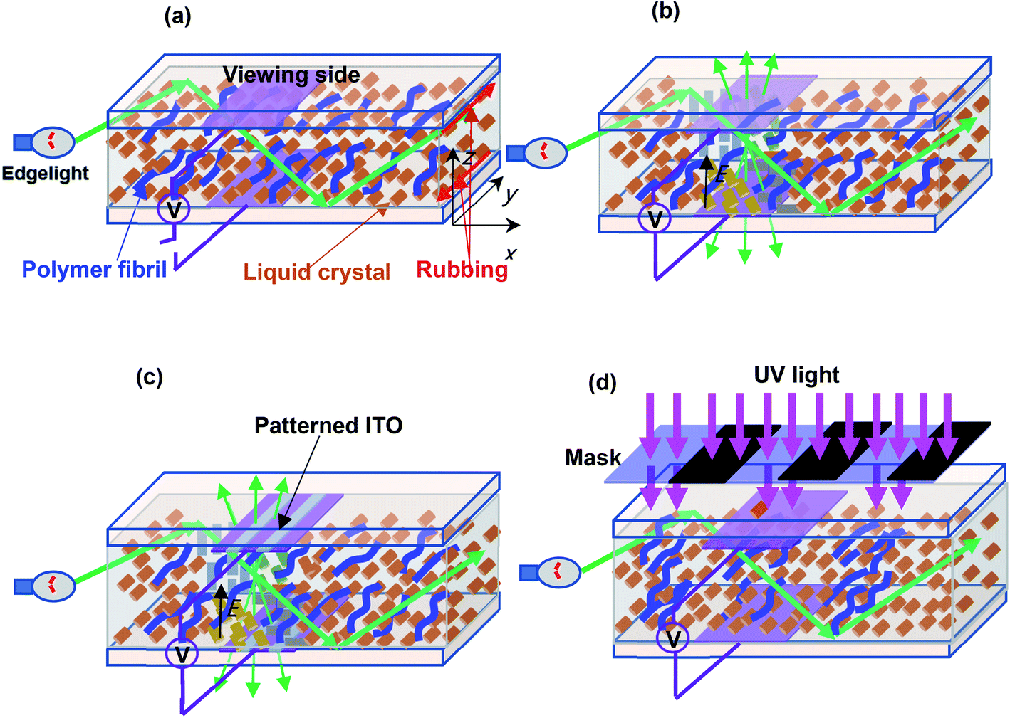 | ||
| Fig. 1 (a) The regular waveguide display in the voltage-off state. (b) The regular waveguide display in the voltage-on state. (c) The patterned electrode waveguide display in the voltage-on state. (d) The patterned photo-polymerization waveguide display. | ||
In the waveguide display LEDs are installed on the edge of the display. The produced light is coupled into the display. When no voltage is applied, the incident light is waveguided through the cell by total internal reflection at the substrate–air interface. No light comes out of the viewing side of the display, as shown Fig. 1(a). When a voltage is applied across the cell in the vertical direction (the z direction), the electric field tries to align the liquid crystal (with a positive dielectric anisotropy) in the vertical direction, while the polymer fibrils try to retain the liquid crystal in the y direction. The direction of the liquid crystal depends on the competition between the aligning effects of the electric field and polymer fibrils. The locations of the fibrils are random. The distance between two neighboring fibrils varied in the micron regime. The reorientation of the liquid crystal between two polymer fibrils depends on the distance between the fibrils.43,44 Under a given voltage, if the distance between two fibrils is large, the liquid crystal tilts more; otherwise; if the distance between two fibrils is small, the liquid crystal tilts less. The random locations of the polymer fibrils produce a random poly-domain structure of the liquid crystal with a length scale comparable to the wavelength of light as shown in Fig. 1(b). The effective refractive index of the liquid crystal depends on its orientation. The incident light encounters different refractive indices in different liquid crystal domains. Therefore it is scattered by the liquid crystal. Some of the scattered light hits on the substrate–air interface with a small incident angle (with respect to the substrate normal), and therefore comes out of the viewing side of the display, as shown in Fig. 1(b).
The light intensity of the display depends on the light scattering of the medium, which in turn depends on the randomness of the liquid crystal domain. In the voltage-off state (dark state) the orientation of the liquid crystal should be as uniform as possible to minimize the scattering. In the voltage-on state (bright state), the orientation of the liquid crystal should be as random as possible to maximize the scattering. Keeping these two criteria in mind, one way to enhance the scattering in the voltage-on state is to use a patterned ITO electrode, as shown in Fig. 1(c). The electrode is patterned into stripes. In the voltage-off state, there is no electric field anywhere inside the cell. Therefore the patterning does not change the orientation of the liquid crystal, and thus the optical property remains the same. In the voltage-on state, in the region, where there is ITO coating and thus there is an electric field, the liquid crystal will reorient under the electric field in the same way as before, while in the region, where there is no ITO coating and thus there is no electric field, the liquid crystal does not reorient. Hopefully this will increase the randomness of the liquid crystal and thus enhance the scattering. Another way to enhance of the scattering in the voltage-on state is to use patterned photo-polymerization, as shown in Fig. 1(d). The photo-mask consists of alternating black and transparent stripes. When the cell is placed under UV light to photo-polymerize the monomer molecules, the photo-mask is put on top of the display facing the UV light. In the region of the cell under the back stripe, the UV light is blocked, and thus no polymer network forms, while in the region of the cell under the transparent stripe, the monomer molecules are polymerized to form a polymer network. After the polymerization, in the voltage-off state, the liquid crystal is uniformly aligned in the aligning rubbing direction, and thus the optical property remains the same. In the voltage-on state, in the region where there is polymer network, the liquid crystal will reorient under the electric field in the same way as before, while in the region where there is no polymer network, the liquid crystal tilts more under the electric field. Therefore, the patterned photo-polymerization will increase the randomness of the liquid crystal and thus enhances the scattering.
2.2 Material formulation, display cell parameter, polymerization condition and measurement
The polymer stabilized liquid crystal is made from 94.5 wt% of nematic liquid crystal BOE-5 (from BOE), which has a positive dielectric anisotropy (Δε > 0), 5 wt% of bifunctional reactive mesogenic monomer RM-257 (from Merck), and 0.5 wt% photo-initiator BME (from PolyScience). The display cell is made from two parallel glass plates with ITO coating. A homogeneous alignment layer polyimide SE 2170 (from Nissan Chemical Industries, Ltd.) is spin coated on top of the ITO, pre-baked at 80 °C, hard baked at 200 °C, and then mechanically rubbed. The cell gap is controlled by 2 μm polymer sphere spacers. The liquid crystal/mixture is filled into the cell by capillary action on a hot plate.When the cell is placed under an LED UV light (365 nm) to photo-polymerize the monomer, the mixture is in nematic phase. The UV light intensity is 7 mW cm−2. The UV irradiation time is 30 m.
A white LED is installed on the edge of the display. The produced light is coupled into the display cell. In most of the experiment, the pattern used for the photolithography of the electrode and photo-polymerization is parallel stripes unless otherwise specified. The LED is installed on the edge of the display parallel to the stripe. Thus the incident light propagation direction is perpendicular to the stripe. A photo-diode detector is used to measure the light intensity coming out of the viewing side of the display, as shown by the inset in Fig. 2. The applied voltage is an AC voltage with 1 kHz frequency.
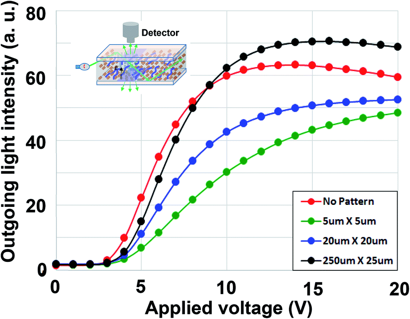 | ||
| Fig. 2 The outgoing light intensity vs. applied voltage curve of the double side patterned electrode waveguide LCDs. | ||
2.3 Patterned electrode waveguide display
Patterned electrode is the first method to enhance the randomness of the liquid crystal. To investigate the effects of patterned electrode on the performance of the waveguide display, we fabricated display cells with a variety of stripe patterned electrodes. We first make display cells with double side (both top and bottom) patterned electrodes. In display D1, the widths of the ITO electrode and the gap between two adjacent electrodes are all 5 μm, denoted as 5 μm × 5 μm. In display D2, the widths of the ITO electrode and the gap between electrodes are all 20 μm, denoted as 20 μm × 20 μm. In display D3, the width of the ITO electrode is 250 μm and the gap between electrodes is 25 μm, denoted as 250 μm × 25 μm. In display D4 (the reference display), the electrode is not patterned. The electrodes on the top and bottom plates are parallel but not aligned. The intensities of the light coming out of the displays are measured under the same condition, as specified previously. The light intensity as a function of applied voltage of the displays is shown in Fig. 2. The performance of displays D1 and D2, with narrow electrode widths and gaps, are worse than that of display D4, without patterned electrode: higher driving voltage and low maximum light intensity. For display D3, with large electrode width, the maximum light intensity is higher, but its driving voltage is higher. The driving voltages, maximum light intensities and contrast ratios of the displays are listed in Table 1. In the displays with double side patterned electrodes, the top and bottom electrode are not aligned, and thus under a given voltage, the produced electric field is smaller and furthermore is not in the cell normal direction (the z direction). The decrease of the electric field probably causes the reduction of the performance of the displays.| Display D1, 5 μm × 5 μm | Display D2, 20 μm × 20 μm | Display D3, 250 μm × 25 μm | Display D4, not patterned | |
|---|---|---|---|---|
| Driving voltage (V) | 20 | 20 | 16 | 12 |
| Maximum light intensity (a.u.) | 39 | 52 | 72 | 63 |
| Contrast ratio | 30 | 30 | 41 | 43 |
In order to avoid the alignment problem of double side patterned electrode, we made display cells with single side (only bottom) patterned electrode. In display S1, the width of the ITO electrode is 5 μm and the gap between two adjacent electrodes is 5 μm, denoted as 5 μm × 5 μm. In display S2, the width of the ITO electrode is 20 μm and the gap between electrodes is 20 μm, denoted as 20 μm × 20 μm. In display S3, the width of the ITO electrode is 250 μm and the gap between electrodes is 25 μm, denoted as 250 μm × 25 μm. In display S4 (the reference display), the electrode is not patterned. The intensities of the light coming out of the displays are measured under the same condition, as specified previously. The light intensity as a function of applied voltage of the displays is shown in Fig. 3. The driving voltages, maximum light intensities and contrast ratios of the displays are listed in Table 2. The maximum light intensity of all the displays with patterned electrode is better than that of the display without patterned electrode. This effect can be explained by that the patterned electrodes increase the randomness of the liquid crystal domain, which results in an increase of the light scattering. The driving voltages of displays S1 and S2 are higher than that of display S4; while the driving voltages of display S3 is almost the same as that of display S4. It seems that under a given voltage, the produced electric field in the displays with narrow electrodes is smaller, and thus the driving voltage is increased. The performance of display S3 with wide electrode is improved.
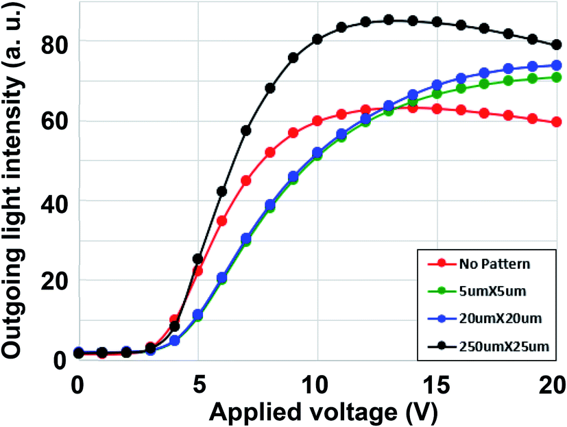 | ||
| Fig. 3 The outgoing light intensity vs. applied voltage curve of the single side patterned electrode waveguide LCDs. | ||
| Display S1, 5 μm × 5 μm | Display S2, 20 μm × 20 μm | Display S3, 250 μm × 25 μm | Display S4, not patterned | |
|---|---|---|---|---|
| Driving voltage (V) | 20 | 20 | 13 | 12 |
| Maximum light intensity (a.u.) | 71 | 74 | 85 | 63 |
| Contrast ratio | 44 | 39 | 53 | 43 |
We measured the dynamic response of display S3. In the measurement, a voltage pulse with 15 V amplitude and 500 ms width is applied, the outgoing light intensity as a function of time is shown in Fig. 4(a). The turn-on time and turn-off time are 0.22 ms and 1.1 ms, respectively, which are superfast and adequate for color sequence operation.
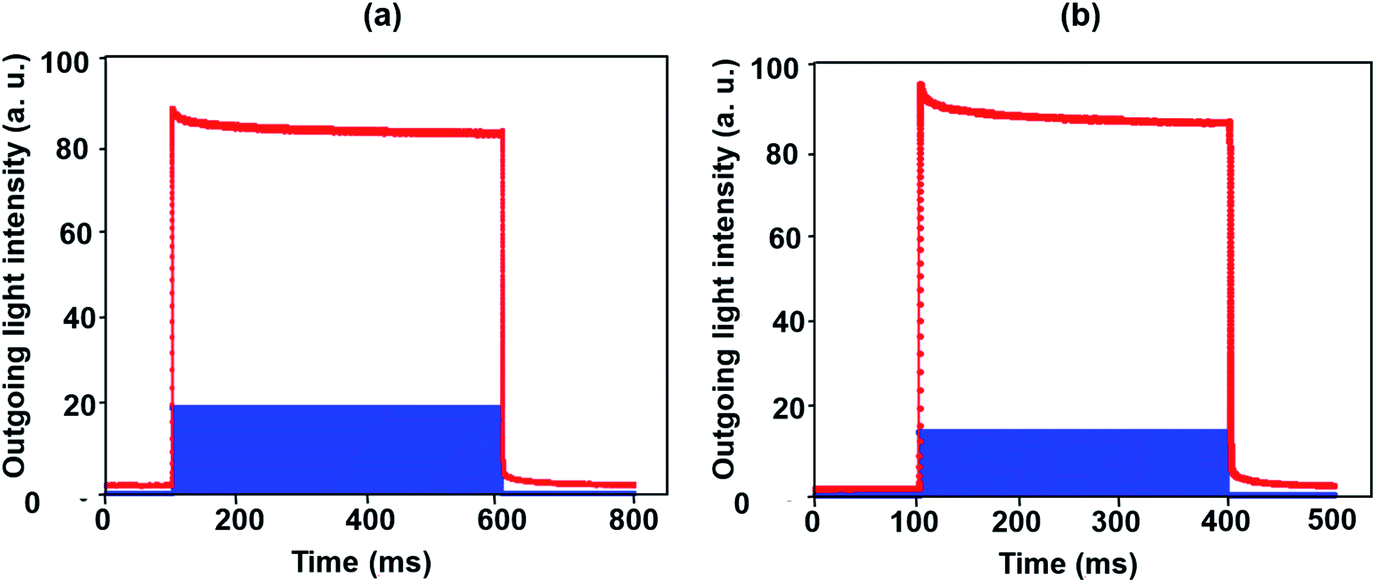 | ||
| Fig. 4 Outgoing light intensity vs. time curves of the waveguide LCDs. (a) Single side patterned electrode waveguide LCD S3. (b) Patterned photo-polymerized waveguide LCD P2. | ||
We studied the switching of the liquid crystal in the displays with single side patterned electrode under a polarizing optical microscope with crossed polarizers. The display is illuminated by a white light which is incident perpendicularly on the display.
As an example, the textures of display S2 under various voltages are shown in Fig. 5. When no voltage is applied, the display appears uniform and has a brownish color, as shown in Fig. 5(a). Note that the dim stripe pattern is probably caused by the different refractive indices between glass and ITO. When 3 V is applied, the appearance of the ITO region changes to orange, as shown in Fig. 5(b), because the liquid crystal is tilted toward the cell normal direction and the optical retardation value is decreased. As the applied voltage is increased, the color of the ITO region shifts to shorter wavelength, and the poly-domain structure of the liquid crystal becomes more obvious. Note that the brightness and color of a spot on the photograph reflects the local effective birefringence at the spot, and does not necessarily indicate the scattered light intensity under LED edgelighting.
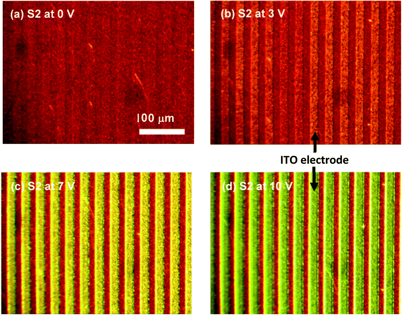 | ||
| Fig. 5 Microphotographs of the single side patterned electrode waveguide display S2. under various voltages: (a) 0 V, (b) 3 V, (c) 7 V and (d) 10 V. The Scale bar is 100 μm | ||
2.4 Patterned photo-polymerization waveguide display
Patterned photo-polymerization is the second method to enhance the randomness of the liquid crystal. We employed patterned photo-polymerization to make the waveguide displays. The photo-masks have patterned stripes consisting of alternating transparent and black stripes. In the polymerization, the region under the transparent stripe is irradiated by UV light. The photo-initiators are converted into free radicals, which initiate the polymerization of the monomers. The region under the black stripe is not irradiated by UV light and no free radicals are produced there. Note, monomers in the un-irradiated region migrate to the irradiated region and are polymerized there. A small amount of free radicals produced in the irradiated region migrate to the un-irradiated region, and initiate the polymerization. In the irradiated region, there are more free radicals and the polymerization is faster. Thus the formed polymer network is denser (higher density of polymer fibrils). In the un-irradiated region, there are less free radicals and the polymerization is slower. Thus the formed polymer network sparser. The time needed for the monomer and free radical to migrate 10 micron is on the order of second. The UV irradiation time is 30 m. During this time, most of the monomers in the un-irradiated region either have migrated to the irradiated region and are polymerized there, or are polymerized locally due to the free radicals coming from the irradiated region. Therefore we expect the amount of residual monomers is small and does not produce a significant hysteresis and long term instability problems. In the fabrication of display P1, the widths of the black stripe and transparent stripe of the used mask are all 5 μm, denoted as 5 μm × 5 μm. In the fabrication of display P2, the widths of the black stripe and transparent stripe of the used mask are all 10 μm, denoted as 10 μm × 10 μm. In the fabrication of display P3, the widths of the black stripe and transparent stripe of the used mask are all 20 μm, denoted as 20 μm × 20 μm. In the fabrication of display P4, the widths of the black stripe and transparent stripe of the used mask are 25 μm and 250 μm, respectively, denoted as 25 μm × 250 μm. In the fabrication of display P5 (the reference display), no mask is used. The intensities of the light coming out of the displays are measured under the same condition, as specified previously. The light intensity as a function of applied voltage of the displays is shown in Fig. 6. The displays made under patterned photo-polymerization are all better than the one made under no mask. The patterned photo-polymerization increases the outgoing light intensity, but does not change the driving voltage. Display P2, made under the 10 μm × 10 μm mask, has the best performance. The driving voltages, maximum light intensities and contrast ratios of the displays are listed in Table 3. The patterned photo-polymerization does not affect the orientation of the liquid crystal in the voltage-off state. Therefore, the outgoing light intensity remains unchanged. Compared with display P5 made under no mask, when a voltage with a given amplitude is applied, the generated electric field in the displays made under masks is not affected by the patterned photo-polymerization. In the region with denser polymer network, the orientation of the liquid crystal changes less, while in the region with sparser polymer network, the orientation of the liquid crystal changes more. Thus the randomness of the liquid crystal is enhanced and the outgoing light intensity is increased. The turn-on and turn-off times of the displays remain unchanged. As an example, the dynamic response of display P2 to a voltage pulse is shown in Fig. 4(b). The amplitude of the pulse is 15 V. The turn-on time is 0.23 ms and the turn-off time is 1.2 ms.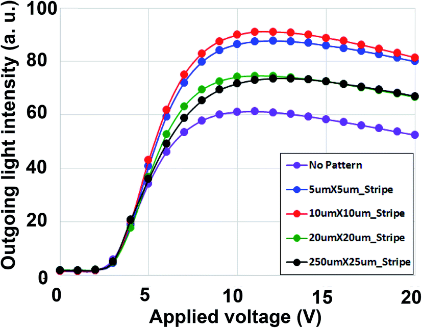 | ||
| Fig. 6 The outgoing light intensity vs. applied voltage curve of the patterned photo-polymerized waveguide LCDs. | ||
| Display P1, 5 μm × 5 μm | Display P2, 10 μm × 10 μm | Display P3, 20 μm × 20 μm | Display P4, 25 μm × 250 μm | Display P5, not patterned | |
|---|---|---|---|---|---|
| Driving voltage (V) | 12 | 11 | 11 | 12 | 12 |
| Maximum light intensity (a.u.) | 88 | 91 | 74 | 73 | 63 |
| Contrast ratio | 53 | 60 | 42 | 44 | 43 |
We also studied the switching of the liquid crystal in the patterned photo-polymerized displays under a polarizing optical microscope. As an example, the textures of display P2 under various voltages are shown in Fig. 7. When no voltage is applied, the textures of the liquid crystal in the two regions are more or less the same and have a brownish color as shown in Fig. 7(a). When 5 V is applied, the textures of the liquid crystal in the two regions becomes different. In the region with sparser polymer network, the liquid crystal is tilted more toward the cell normal direction and the optical retardation value is decreased, and thus appears greener, as shown in Fig. 7(b). As the applied voltage is increased, the contrast between the textures of the two regions increases, as shown in Fig. 7(c) and (d). Note that the brightness and color of a spot on the photograph reflects the local effective birefringence at the spot, and does not necessarily indicate the scattered light intensity under LED edgelighting.
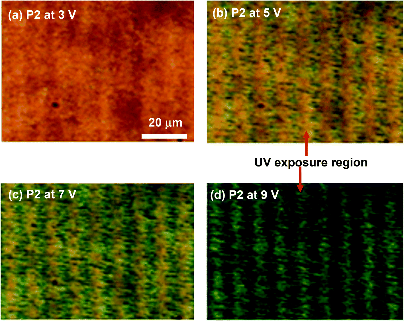 | ||
| Fig. 7 The microphotographs of the patterned photo-polymerized waveguide LCD P2 under various applied voltages: (a) 0 V, (b) 5 V, (c) 7 V, and (d) 9 V. The scale bar is 20 μm. | ||
The performance of the patterned photo-polymerized displays depends on the direction of the stripes with respect to the incident light propagation direction. There are two possible geometries. In the first geometry, called perpendicular geometry, the LED is installed on the edge of the display parallel to the stripe, and thus the stripe is perpendicular to the incident light propagation direction. In the experiments whose results are reported in the previous paragraphs, this geometry is used. In the second geometry, called parallel geometry, the LED is installed on the edge of the display perpendicular to the stripe, and thus the stripe is parallel to the incident light propagation direction. The results of display P2 under these two geometries are shown in Fig. 8. The outgoing light intensity is much higher in the perpendicular geometry, because when light propagates through the display, the encountered refractive index varies more. The contrast ratio in the perpendicular geometry is 60, while the contrast ratio in the parallel geometry is only 12.
 | ||
| Fig. 8 The outgoing light intensity vs. applied voltage curve of the patterned photo-polymerized waveguide display P2 under two lighting conditions: light propagation direction parallel and perpendicular to the stripe, respectively. | ||
In addition, we fabricated a patterned photo-polymerized waveguide display using a mask with 10 μm × 10 μm square pattern and study its electro-optical properties. The outgoing light intensity as a function of applied voltage of the display is shown in Fig. 9. For the purpose of comparison, the light intensity as a function of applied voltage of display P3 with stripe is also shown in the figure. Their behaviors are almost the same, except that at 0 V the light intensity of the display with square pattern is a slightly high, due to higher randomness of the liquid crystal in this display. The small difference has a medium impact on the contrast ratio. The contrast ratio of the display with the square pattern is 50, while the contrast ratio of the display with stripe pattern is 60.
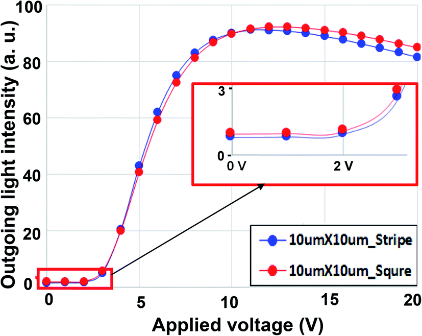 | ||
| Fig. 9 The outgoing light intensity vs. applied voltage curve of the stripe and square patterned photo-polymerized waveguide LCDs. | ||
We also studied the wavelength dependence of the intensity of the light coming out of display P2. We first measured the spectrum of the light directly from the white LED. The result is shown by curve (a) in Fig. 10. It has two peaks: one around 450 nm and the other one around 550 nm. We then measured the spectrum of the light coming out of the display. We calculate the ratio by dividing the spectrum (b) by spectrum (a). The ratio is the scattering efficiency of the material. It decreases with increasing wavelength. This is caused by the decrease of the birefringence of the liquid crystal with increasing wavelength. In single scattering regime, the scattering efficiency is proportional to the square of the birefringence. In the wavelength region around 500 nm, the large fluctuation of the ratio is caused by electronic noise because of low light intensity.
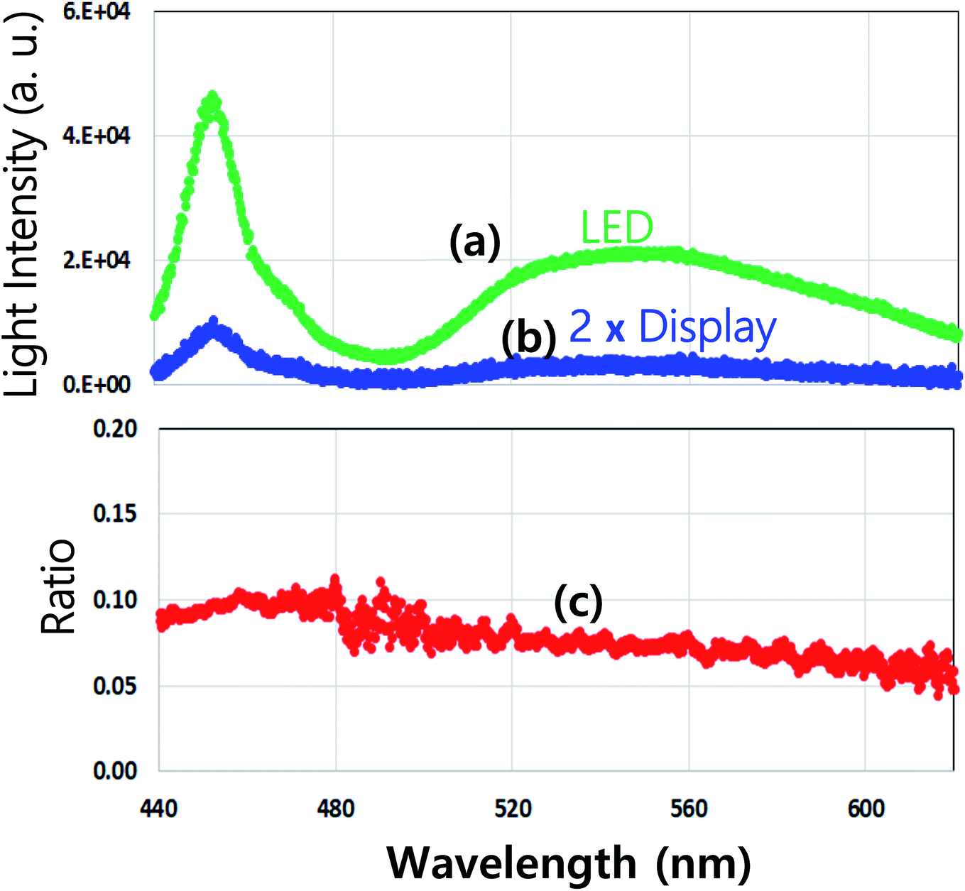 | ||
| Fig. 10 (a) Spectrum of the white LED. (b) Spectrum of the light coming out of display P2. (c) Ratio between (b) and (a). | ||
To show the improvement of patterned photo-polymerized waveguide display over the un-patterned photo-polymerized waveguide display, we fabricated a display with patterned ITO with “LCI” characters. The display is polymerized under the mask with the 10 μm × 10 μm stripe pattern. The display can be operated in either transparent display mode,45–47 or direct view display mode.48 To demonstrate the display in transparent display mode, a picture of Kent State University is placed behind them. When no voltage is applied, the display is very transparent with a transmittance about 90%, and the picture behind them can be seen clearly, as shown in Fig. 11(a). When 15 V is applied, the ITO region with “LCI” characters becomes bright, while the region without ITO remains transparent, as shown in Fig. 11(b). To demonstrate the display in direct view display mode, a black absorbing layer is placed behind it. When no voltage is applied, the display appears black, as shown in Fig. 11(c). When 15 V is applied, the ITO region with “LCI” characters becomes bright, while the region without ITO remains dark, as shown in Fig. 11(d).
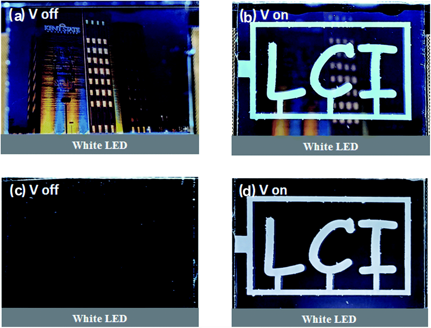 | ||
| Fig. 11 Photographs of the patterned photo-polymerized waveguide displays in transparent display mode (a) and (b): in transparent display mode (c) and (d): in direct view display mode. | ||
3. Discussion and conclusion
We developed patterned light waveguide liquid crystal displays. We designed two patterning methods to improve the performance of normal (un-patterned) waveguide liquid crystal display. The first method is patterning electrode. The second method is patterning photo-polymerization. Both methods can improve the brightness of the waveguide display, and as well retain the merits of highly transparent voltage-off state, superfast response time and active matrix compatible driving voltage. The patterning electrode method can enhance the randomness of the liquid crystal, resulting in a higher brightness. However, it has a drawback that the driving voltage is increased, because under a given voltage, the electric field is decreased. The patterning photo-polymerization method can increase the randomness of the liquid crystal and thus the brightness, and contrast ratio of the waveguide display without the tradeoff of higher driving voltage. Therefore it is better than the patterning electrode method. Driving voltage is an important issue for thin-film-transistor active matrix liquid crystal display. As shown in Fig. 6, for the patterned photo-polymerized waveguide display, the light intensity begins to increase when the applied voltage is increased above 3 V, which is the threshold voltage, and saturates at 10 V, which is the saturation voltage. The difference between these two voltages is 7 V, which is compatible with TFT technology. The driving voltage can be decreased by using thinner cell, lower polymer concentration and a liquid crystal with a larger dielectric anisotropy.It is not fully understood how the striped structure with scale on the order of tens microscope contributes to the enhancement of the scattering of light with wavelength around half micron. There are two possible mechanisms that enhance the light scattering. The first mechanism is that the patterning increases the randomness of the effective refractive index of the material. In the region exposed to UV light, the formed polymer network is denser, where the liquid crystal rotates less under a given voltage; while in the region not exposed to UV light, the formed polymer network is sparser, where the liquid crystal rotates more under a given voltage. Furthermore, in the transitional region between the UV exposed and unexposed region, the polymer network density changes gradually, which also increases the randomness. The second mechanism is light diffraction. Because of the periodic striped structure, there is some kind of diffraction which produces a constructive interference between the scattered light from the stripes, which increases the intensity of light coming of the display.
Light efficiency is an important issue in displays. Regular liquid crystal displays have a very low light efficiency about 8% because they use two polarizer and a color filters which absorb light. The waveguide display does not absorb light and thus in principle have a higher light efficiency. However, it may have a low light extraction efficiency if the unscattered light leaks out of the display on the edges. In order to increase its light efficiency, the unscattered light should be recycled by installing reflectors on the edges of the display. At this moment we do not know the exact light efficiency because of the lack of the necessary measurement equipment.
In summary, the patterned photo-polymerized waveguide liquid crystal display does not use polarizers. Furthermore it does not use color filter. It has superfast sub-millisecond switching time. Color sequence can be used to generate full color images. In the voltage-off state, it has a transmittance close to 90%, much higher than the transmittance, about 8%, of regular liquid crystal displays. It is very suitable for head-up vehicle displays and augmented displays.
Conflicts of interest
There are no conflicts to declare.Acknowledgements
This research was supported by BOE Technology Group Co.References
- J.-H. Lee, D. N. Liu and S.-T. Wu, Introduction to flat panel displays, John Wiley & Sons, 2008, vol. 20 Search PubMed.
- E. Lueder, Liquid crystal displays: addressing schemes and electro-optical effects, John Wiley & Sons, 2010 Search PubMed.
- D.-K. Yang and S.-T. Wu, Fundamentals of liquid crystal devices, John Wiley & Sons, 2014 Search PubMed.
- M. S. Kim, et al., Liquid Crystals for Superior Electro-Optic Performance Display Device with Power-Saving Mode, Adv. Opt. Mater., 2018, 6(11), 1800022 CrossRef.
- M. Schadt and W. Helfrich, Voltage-dependent optical activity of a twisted nematic liquid crystal, Appl. Phys. Lett., 1971, 18(4), 127–128 CrossRef CAS.
- R. A. Soref, Field effects in nematic liquid crystals obtained with interdigital electrodes, J. Appl. Phys., 1974, 45(12), 5466–5468 CrossRef CAS.
- M. Oh-e and K. Kondo, Electro-optical characteristics and switching behavior of the in-plane switching mode, Appl. Phys. Lett., 1995, 67(26), 3895–3897 CrossRef CAS.
- M. Oh-e and K. Kondo, Response mechanism of nematic liquid crystals using the in-plane switching mode, Appl. Phys. Lett., 1996, 69(5), 623–625 CrossRef CAS.
- M. Ohta, M. Oh-e and K. Kondo, Development of super-TFT-LCDs with in-plane switching display mode, Proc. of Asia Display, 1995, vol. 95, pp. 707–710 Search PubMed.
- R. A. Soref, Field effects in nematic liquid crystals obtained with interdigital electrodes, J. Appl. Phys., 1974, 45(12), 5466–5468 CrossRef CAS.
- M. F. Schiekel and K. Fahrenschon, Deformation of nematic liquid crystals with vertical orientation in electrical fields, Appl. Phys. Lett., 1971, 19(10), 391–393 CrossRef CAS.
- A. Takeda, S. Kataoka, T. Sasaki, H. Chida, H. Tsuda, K. Ohmuro, Y. Koike, T. Sasabayashi and K. Okamoto, Super-High Image Quality Multi-Domain Vertical Alignment LCD by New Rubbing-Less Technology, SID Symposium Digest of Technical Papers, 1998, 29, 1077 CrossRef.
- S. H. Lee, S. L. Lee and H. Y. Kim, Electro-optic characteristics and switching principle of a nematic liquid crystal cell controlled by fringe-field switching, Appl. Phys. Lett., 1998, 73(20), 2881–2883 CrossRef CAS.
- Y. M. Jeon, I. S. Song, S. H. Lee, H. Y. Kim, S. Y. Kim and Y. J. Lim, P-165: optimized electrode design to improve transmittance in the fringe-field switching (FFS) liquid crystal cell, SID Symposium Digest of Technical Papers, 2005, 36(1), 328–331 CrossRef CAS.
- A. Moheghi, et al., 54.3: PSCT for Switchable Transparent Liquid Crystal Displays, SID Symposium Digest of Technical Papers, 2015, 46(1), 817–820 CrossRef.
- S. H. Wu, C. H. Chen and J. T. Lian, 17-inch high performance transparent Display using newly scattering-type surface anchoring LC, SID Symposium Digest of Technical Papers, 2018, 1741–1743 CrossRef.
- T. Iino, Head-up display apparatus for automotive vehicle, US Pat., 4,908,611, 13 Mar. 1990.
- M. H. Schuck, D. J. McKnight and K. M. Johnson, Automotive head-up display using liquid-crystal-on-silicon displays, J. Soc. Inf. Disp., 1997, 5(1), 33–35 CrossRef.
- M. Hähl, Color head-up display, in particular for a vehicle, US Pat., 7,034,778, 25 Apr. 2006.
- J. F. Szczerba, D. Cui, and T. A. Seder, Dynamic vehicle system information on full windshield head-up display, US Pat., 8,912,978, 16 Dec. 2014.
- P. Thomas and W. M. David, Augmented reality: an application of heads-up display technology to manual manufacturing processes, Hawaii International Conference on System Sciences, 1992 Search PubMed.
- I. N. Robinson, M. April Slayden and G. G. Daniel, Augmented reality display system and method of display, US Pat., 9,164,581, 20 Oct. 2015.
- G. Li, et al., Holographic display for see-through augmented reality using mirror-lens holographic optical element, Opt. Lett., 2016, 41(11), 2486–2489 CrossRef.
- W. J. Westerinen, et al., Augmented reality light guide display, US Pat., 9,558,590, 31 Jan. 2017.
- J. Kim, et al., Foveated AR: dynamically-foveated augmented reality display, ACM Transactions on Graphics, 2019, 38(4), 1–15 Search PubMed.
- S. -W. Oh, et al., Optical and thermal switching of liquid crystals for self-shading windows, Adv. Sustainable Syst., 2018, 2(5), 1700164 CrossRef.
- A. Ronald, Optical waveguide display panel, US Pat., 3,871,747, March 18, 1975.
- D. H. Staelin, Method and apparatus utilizing waveguide and polarized light for display of dynamic images, US Pat., 4,822,145A, May 14, 1986.
- H. Ma, A. K. -Y. Jen and L. R. Dalton, Polymer-based optical waveguides: materials, processing, and devices, Adv. Mater., 2002, 14(19), 1339–1365 CrossRef CAS.
- H. Yuan and P. Palffy-Muhoray, Liquid-crystal display-demonstration of the waveguide-based LCD, J. Soc. Inf. Disp., 1999, 7(4), 269–272 CrossRef.
- H. Yuan and P. -M. Peter, Demonstration of the waveguide-based LCD, J. Soc. Inf. Disp., 1999, 7(4), 269–271 CrossRef.
- Y.-H. Shin, N.-S. Oh and S.-B. Kwon, Electro-optical properties of vertically aligned polymer network liquid crystals for normally transparent light shutters, Mol. Cryst. Liq. Cryst., 2017, 644(1), 130–136 CrossRef CAS.
- Y.-H. Shin, et al., A Normally Transparent Polymer Dispersed Liquid Crystal Developed by Using a Two-Step UV Exposure Method for Transparent Flexible Displays, Sci. Adv. Mater., 2016, 8(2), 369–375 CrossRef CAS.
- N.-S. Oh, et al., High performance dye-doped emulsion type PDLC for transmittance variable devices, Mol. Cryst. Liq. Cryst., 2017, 644(1), 137–144 CrossRef CAS.
- Y.-H. Shin, N.-S. Oh and S.-B. Kwon, Electro-optical properties of normally transparent polymer dispersed liquid crystal cells with polymer wall and network structure, Mol. Cryst. Liq. Cryst., 2017, 647(1), 415–421 CrossRef CAS.
- K. Okuyama, T. Nakahara, Y. Numata, T. Nakamura, M. Mizuno, H. Sugiyama, S. Nomura, S. Takeuchi, Y. Oue, H. Kato, S. Ito, A. Hasegawa, T. Ozaki, M. Douyou, T. Imai, K. Takizawa and S. Matsushima, Highly transparent LCD using new scattering-type liquid crystal with field sequential color edge light, SID Symposium Digest of Technical Papers, 2017, 1166–1169 CrossRef CAS.
- C. Meng, et al., Color-switchable liquid crystal smart window with multi-layered light guiding structures, Opt. Express, 2019, 27(9), 13098–13107 CrossRef CAS.
- L. Wang, et al., P-89: Development of Waveguide Liquid Crystal Display for Transparent Display Applications, SID Symposium Digest of Technical Papers, 2019, 50(1), 1573–1575 CrossRef CAS.
- M. Born and E. Wolf, Principles of Optics: Electromagnetic Theory of Propagation, Interference and Diffraction of Light, Cambridge University, 1999 Search PubMed.
- S. Lal, S. Link and N. J. Halas, Nano-optics from sensing to waveguiding, Nat. Photonics, 2007, 1(11), 641 CrossRef CAS.
- X. C. Zhou, G. K. Qin, L. Wang, Z. Chen, X. G. Xu, Y. M. Dong, A. Moheghi and D. K. Yang, Full color waveguide liquid crystal display, Opt. Lett., 2017, 42(18), 3706–3709 CrossRef CAS.
- R. A. M. Hikmet and H. M. J. Boots, Domain structure and switching behavior of anisotropic gels, Phys. Rev. E: Stat. Phys., Plasmas, Fluids, Relat. Interdiscip. Top., 1995, 51(6), 5824 CrossRef CAS.
- D.-K. Yang, Polymer-stabilized liquid crystal displays, Progress in Liquid Crystal Science and Technology: In Honor of Shunsuke Kobayashi's 80th Birthday, 2013, pp. 597–628 Search PubMed.
- D.-K. Yang, et al., Modeling aligning effect of polymer network in polymer stabilized nematic liquid crystals, J. Appl. Phys., 2013, 114(24), 243515 CrossRef.
- E. Downing, et al., A three-color, solid-state, three-dimensional display, Science, 1996, 273(5279), 1185–1189 CrossRef CAS.
- C. W. Hsu, et al., Transparent displays enabled by resonant nanoparticle scattering, Nat. Commun., 2014, 5, 3152 CrossRef.
- S. -H. K. Park, et al., Transparent and photo-stable ZnO thin-film transistors to drive an active matrix organic-light-emitting-diode display panel, Adv. Mater., 2009, 21(6), 678–682 CrossRef CAS.
- P. Nolan, Reflective mode PDLC displays-paper white display, IDRC'93 Technical Digest, 1993, pp. 397–400 Search PubMed.
| This journal is © The Royal Society of Chemistry 2020 |