
 Open Access Article
 This Open Access Article is licensed under a Creative Commons Attribution-Non Commercial 3.0 Unported Licence
Cu oxidation kinetics through graphene and its effect on the electrical properties of graphene†
Min-Sik Kim‡
a,
Ki-Ju Kim‡a,
Minsu Kima,
Sangbong Leea,
Kyu Hyun Leec,
Hyeongkeun Kimc,
Hyun-Mi Kim*bc and
Ki-Bum Kim *ab
*ab
aDepartment of Materials Science and Engineering, Seoul National University, 1 Gwanak-ro, Gwanak-gu, Seoul, 08826, South Korea
bResearch Institute of Advanced Materials, Seoul National University, 1 Gwanak-ro, Gwanak-gu, Seoul, 08826, South Korea. E-mail: hyunmi@snu.ac.kr; kibum@snu.ac.kr
cKorea Electronics Technology Institute, 25 Saenari-ro, Bundang-gu, Seongnam-si, Gyeonggi-do 13509, South Korea
First published on 28th September 2020
Abstract
The oxidation kinetics of Cu through graphene were evaluated from the surface coverage of Cu oxide (Fox) by varying the oxidation time (tox = 10–360 min) and temperature (Tox = 180–240 °C) under an air environment. Fox, as a function of time, well followed the Johnson–Mehl–Avrami–Kolmogorov equation; thus, the activation energy of Cu oxidation was estimated as 1.5 eV. Transmission electron microscopy studies revealed that Cu2O formed on the top of the graphene at grain boundaries (G-GBs), indicating that Cu2O growth was governed by the out-diffusion of Cu through G-GBs. Further, the effect of Cu oxidation on graphene quality was investigated by measuring the electrical properties of graphene after transferring. The variation of the sheet resistance (Rs) as a function of tox at all Tox was converted into one curve as a function of Fox. Rs of 250 Ω sq−1 was constant, similar to that of as-grown graphene up to Fox = 15%, and then increased with Fox. The Hall measurement revealed that the carrier concentration remained constant in the entire range of Fox, and Rs was solely related to the decrease in the Hall mobility. The variation in Hall mobility was examined according to the graphene percolation probability model, simulating electrical conduction on G-GBs during Cu2O evolution. This model well explains the constant Hall mobility within Fox = 15% and drastic Fox degradation of 15–50% by the concept that the electrical conduction of graphene is disconnected by Cu2O formation along with the G-GBs. Therefore, we systematically developed the oxidation kinetics of Cu through graphene and simultaneously examined the changes in the electrical properties of graphene.
Introduction
Since the experimental discovery of graphene by the scotch-tape method in 2004,1 high-quality single layer graphene has been grown from various hydrocarbon precursors by chemical vapor deposition (CVD) on Cu film. As a metal catalyst for the CVD process,2,3 Cu foil not only dissociates hydrocarbon precursors but also self-limits the growth of graphene by its extremely low solubility for carbon.2,4 Nevertheless, under the random nucleation and growth process of CVD, the graphene layer has a polycrystalline nature on the Cu surface. The graphene grain boundaries (G-GBs) inherently inhibit charge transport, severely degrading the mobility of charge carriers.5–8 Moreover, the G-GBs significantly affect other physical properties including, the mechanical strength and gas-molecule impermeability of graphene.9,10 To grow a graphene layer with large grain size, researchers have carefully tuned the graphene-growth conditions.11–13 Furthermore, the characterization of the G-GBs, such as grain size linked to the physical properties of graphene, has been a major topic of concern.Raman spectroscopy is among the most efficient characterization methods of graphene. The D peak (which appears at ∼1350 cm−1 on the Raman spectrum) represents the breakage of the sp2 bond by structural defects in the graphene lattice.14 Raman spectroscopy provides various quantitative information of graphene, such as the number of graphene layers (from the intensity ratio of the G and D peaks) and doping amount (from the shift of the G or 2D peak).15–17 However, Raman spectroscopy cannot provide information over the entire sample area because the laser beam size is limited to a few μm.2 Furthermore, the graphene must be transferred to an SiO2 substrate for accurate analysis. Transmission electron microscopy (TEM) is clearly advantageous because its atomic resolution enables direct observation of the graphene lattice.18 However, sample preparation is quite difficult, and the observed area is extremely small. The measurement of the electrical properties of graphene requires the transfer of graphene on the insulating substrate for fabricating a device. Because various defects (e.g., wrinkles, cracks, holes, and organic residues) are introduced during the transfer process,19 the measured property cannot be correlated with the quality of the as-grown graphene. Therefore, a method for the analysis of the as-grown graphene on Cu is required for proper tuning of the graphene-growth condition.
In this respect, the oxidation of Cu underlying graphene has been proposed by several researchers as a useful method to simply observe the graphene grain.20–26 Because the hexagonal arrangement of carbon atoms in graphene is sufficiently compact to inhibit the penetration of oxygen (and consequently the oxidation of Cu),27 Cu is selectively oxidized by oxidizing species, such as OH− or O−, which penetrate the G-GBs.22–24 These radicals are typically dissociated from H2O at elevated temperatures (approximately 200 °C) or under UV exposure.23,24 Energy calculations using density functional theory and TEM observations have shown that oxygen radicals penetrate the G-GBs without bond breaking. Oxygens penetrating the boundary at room temperature was reported to form Cu oxide at the graphene–Cu interface.25 Moreover, the lateral diffusion of oxygen at the graphene–Cu interface is hindered by van der Waals forces between the Cu and graphene.26 Although the results of oxidation kinetics depend on the states of the graphene (e.g., grain size, shape, and stitching between grains) and the Cu foil (e.g., crystallographic orientation),28 the oxidation of Cu through the grain boundary of the graphene layer has not been systematically investigated. Furthermore, the extent to which Cu oxidation damages the electrical property of graphene is unknown.
Here, Cu oxidation through graphene was investigated as a function of temperature (180–240 °C) and time (10–360 min). The oxidation kinetics of Cu through the G-GBs was determined based on the Cu oxide coverage that was quantitatively estimated from the optical microscope (OM) images. To investigate the effect of Cu oxidation on graphene quality, all graphene samples were transferred on a polyethylene terephthalate (PET) film and then the electrical properties (i.e., sheet resistance, Hall mobility, and charge carrier density) of these samples were measured as a function of oxidation time and temperature by Hall measurement. We correlated the extent of Cu oxidation and electrical properties of graphene; these results enable the prediction of electrical properties through graphene visualization by Cu oxidation.
Results and discussion
Characterization of as-grown graphene
The single layer graphene (SLG) was synthesized on the Cu foil by rapid thermal chemical vapor deposition (RTCVD) at 1025 °C for 1000 s. As shown in ESI S-I,† no discernible features, e.g., G-GB or other defects, were observed on the as-grown SLG film by the OM image analysis. The sheet resistance (Rs), sheet carrier density (ns), and Hall mobility (μ) of the SLG transferred on the PET substrate were 254 Ω sq−1, 1.5 × 1013 cm−2, and 1572 cm2 V−1 s−1, respectively. The ns of the as-grown SLG was found to be one order of magnitude higher than that of the pristine graphene (without intentional doping) because of the molecular p-type doping by the adsorption of imidazole during the wet etching of the Cu foil.29Cu oxidation kinetics on graphene/Cu foil structure
The as-grown SLG on Cu foil was heat treated under air atmosphere to investigate the Cu oxidation behavior through the graphene. Fig. 1 shows the OM images at each oxidation temperature (Tox) and oxidation time (tox); Fig. 1(a)–(d), (e)–(h), (i)–(l), and (m)–(p) show the OM images at 180 °C, 200 °C, 220 °C, and 240 °C, respectively. Early heat-treated samples at 180 °C/60 min, 200 °C/30 min, and 220 °C/15 min (Fig. 1(a), (e), and (i), respectively) show dark contrasts at the line expected with G-GBs. Upon increasing the tox, the dark contrasts not only delineate the grain boundaries of graphene (Fig. 1(c), (g), and (j)) but also increase their line width (Fig. 1(d), (h), and (k), respectively). Eventually, the bright area, presumed to be a graphene grain, is isolated, as shown in Fig. 1(l). At 240 °C, the graphene grain seems to isolate after exposure to air for 10 min and the size of the bright area decreases with increasing tox. Notably, some samples with similar oxidation morphologies, such as those treated at 180 °C/240 min, 200 °C/120 min, and 220 °C/30 min that are illustrated in Fig. 1(c), (g), and (j), respectively, show that the tox tends to decrease to half its value with Tox by only 20 °C. As shown in ESI S-II,† the energy-dispersive X-ray spectroscopy (EDS) mapping image of sample oxidized at 220 °C for 1 hour clearly shows that a large amount of oxygen is detected in a dark area in OM image which indicates the dark area is Cu oxide. Previous reports23,24 on the composition analysis of Cu oxidation under graphene using TEM also suggested that the dark contrast in OM images corresponds to Cu oxide. Therefore, the Cu oxidation, dark contrasts on OM image, begins at the G-GBs and progresses to the periphery of the G-GBs.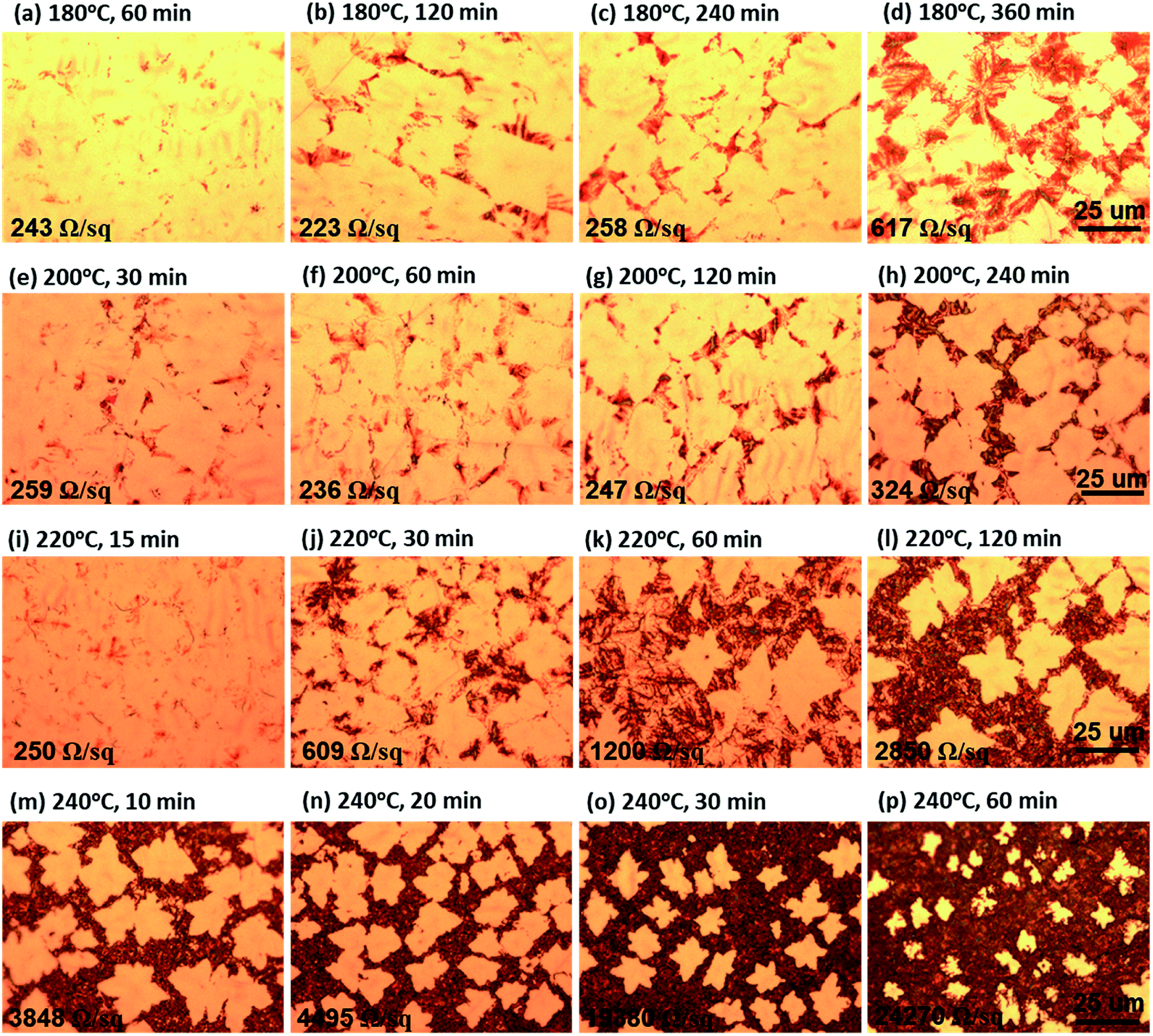 | ||
| Fig. 1 Optical microscope images of the as-grown graphene after the oxidation at (a)–(d) 180 °C, (e)–(h) 200 °C, (i)–(l) 220 °C, and (m)–(p) 240 °C. | ||
The dark area in the sample oxidized at 200 °C for 120 min was analyzed using cross-sectional TEM (Fig. 2). The cross-sectional TEM samples were prepared perpendicular to the dark lines. Bright-field scanning TEM (STEM) revealed a radially grown morphology on the flat Cu surface (Fig. 2(a)). From the indexing of the selected area diffraction pattern (Fig. 2(c)) and composition analysis of energy dispersive spectroscopy (EDS, Fig. 2(e)), the species was determined as Cu2O (space group: Pn![[3 with combining macron]](https://www.rsc.org/images/entities/char_0033_0304.gif) m, a = 4.288 Å). Judging from the low contrast in the high-angle annular dark field (HAADF) STEM images (Fig. 2(b)), the Cu2O had a lower mass density than the Cu substrate. Therefore, the interface between Cu2O and Cu was very clearly defined. The high resolution TEM (HRTEM) images in this area clarified the graphene layer at the Cu–Cu2O interface with an opening at the center (marked by arrows in Fig. 2(d)). The graphene layer was also found under other Cu2O particles (see ESI S-III†). The semi-circular shape of the Cu2O and graphene opening at the center of the interface indicate that Cu2O is formed from a point source of Cu. Furthermore, graphene existence between Cu2O and Cu evidenced that the Cu2O grew by out-diffusion of Cu.30 Indeed, Cu oxidation predominantly occur by the diffusion of Cu cations through Cu oxide.31,32 However, these results contradict a few previous reports, which claim that Cu2O nucleates and grows by oxygen in-diffusion through graphene at the graphene–Cu interface.23,24 According to these previous reports, oxygen atoms dissociate from H2O at the graphene vacancies and GBs then penetrate the G-GBs and form Cu2O at the graphene–Cu interface.24 The randomly oriented and shaped graphene grains are stitched together, forming abundant pentagon, heptagon, and other non-hexagonal carbon rings at the G-GBs.33 G-GBs with imperfect stitching and voids would crack during the CVD process. We believe that Cu2O nucleation was promoted at the non-hexagonal carbon rings or in the imperfect-stitching region of G-GBs but was suppressed at the relatively stable grain boundary. For instance, at 180 °C after 240 min of oxidation, the line width of the grown Cu2O reached 10 μm (Fig. 1(c)), and these locations are considered as the non-hexagonal carbon rings or imperfect-stitching; however, at certain G-GBs where relatively stable G-GBs, still no Cu2O was formed. We surmise that the initial nucleation process of Cu2O was generated by oxygen in-diffusion through the G-GBs as previously reported but that Cu2O grew by the dominant out-diffusion of Cu cations at the G-GBs. Fig. 2(f) shows the schematic sequence of Cu oxidation through graphene based on the results of the current study. During the oxidation, Cu oxide was initially formed at G-GB and further growth was proceeded by out-diffusion of Cu through the Cu oxide. Otherwise, if Cu oxide growth was proceeded by in-diffusion of oxygen to G-GBs, not by out-diffusion of Cu cation, Cu oxide would be encapsulated by the graphene layer. Consequently, the graphene layer undergoes tensile stress generated by 1.7 times of volume expansion during Cu oxide formation, and the estimated strain of graphene is about 80% based on Fig. 3(a). Considering fracture occurs on PMMA and PDMS supported graphene only about 8% of strain during the tensile test,34,35 it seems impossible to survive graphene without fracture during Cu oxide formation. However, no significant Rs change is observed even if almost G-GBs have been decorated by Cu2O (Fig. 1(c), (g) and (i)). Moreover, few samples of graphene seem to be isolated by grown Cu2O, but the measured Rs shows that graphene samples are still electrically connected (Fig. 1(d), (h), (k), and (m)). Therefore, Cu oxide growth proceeds without further graphene damage caused by the volume expansion during Cu2O formation because of oxidation proceeds by out-diffusion of Cu cation through formed Cu2O.
m, a = 4.288 Å). Judging from the low contrast in the high-angle annular dark field (HAADF) STEM images (Fig. 2(b)), the Cu2O had a lower mass density than the Cu substrate. Therefore, the interface between Cu2O and Cu was very clearly defined. The high resolution TEM (HRTEM) images in this area clarified the graphene layer at the Cu–Cu2O interface with an opening at the center (marked by arrows in Fig. 2(d)). The graphene layer was also found under other Cu2O particles (see ESI S-III†). The semi-circular shape of the Cu2O and graphene opening at the center of the interface indicate that Cu2O is formed from a point source of Cu. Furthermore, graphene existence between Cu2O and Cu evidenced that the Cu2O grew by out-diffusion of Cu.30 Indeed, Cu oxidation predominantly occur by the diffusion of Cu cations through Cu oxide.31,32 However, these results contradict a few previous reports, which claim that Cu2O nucleates and grows by oxygen in-diffusion through graphene at the graphene–Cu interface.23,24 According to these previous reports, oxygen atoms dissociate from H2O at the graphene vacancies and GBs then penetrate the G-GBs and form Cu2O at the graphene–Cu interface.24 The randomly oriented and shaped graphene grains are stitched together, forming abundant pentagon, heptagon, and other non-hexagonal carbon rings at the G-GBs.33 G-GBs with imperfect stitching and voids would crack during the CVD process. We believe that Cu2O nucleation was promoted at the non-hexagonal carbon rings or in the imperfect-stitching region of G-GBs but was suppressed at the relatively stable grain boundary. For instance, at 180 °C after 240 min of oxidation, the line width of the grown Cu2O reached 10 μm (Fig. 1(c)), and these locations are considered as the non-hexagonal carbon rings or imperfect-stitching; however, at certain G-GBs where relatively stable G-GBs, still no Cu2O was formed. We surmise that the initial nucleation process of Cu2O was generated by oxygen in-diffusion through the G-GBs as previously reported but that Cu2O grew by the dominant out-diffusion of Cu cations at the G-GBs. Fig. 2(f) shows the schematic sequence of Cu oxidation through graphene based on the results of the current study. During the oxidation, Cu oxide was initially formed at G-GB and further growth was proceeded by out-diffusion of Cu through the Cu oxide. Otherwise, if Cu oxide growth was proceeded by in-diffusion of oxygen to G-GBs, not by out-diffusion of Cu cation, Cu oxide would be encapsulated by the graphene layer. Consequently, the graphene layer undergoes tensile stress generated by 1.7 times of volume expansion during Cu oxide formation, and the estimated strain of graphene is about 80% based on Fig. 3(a). Considering fracture occurs on PMMA and PDMS supported graphene only about 8% of strain during the tensile test,34,35 it seems impossible to survive graphene without fracture during Cu oxide formation. However, no significant Rs change is observed even if almost G-GBs have been decorated by Cu2O (Fig. 1(c), (g) and (i)). Moreover, few samples of graphene seem to be isolated by grown Cu2O, but the measured Rs shows that graphene samples are still electrically connected (Fig. 1(d), (h), (k), and (m)). Therefore, Cu oxide growth proceeds without further graphene damage caused by the volume expansion during Cu2O formation because of oxidation proceeds by out-diffusion of Cu cation through formed Cu2O.
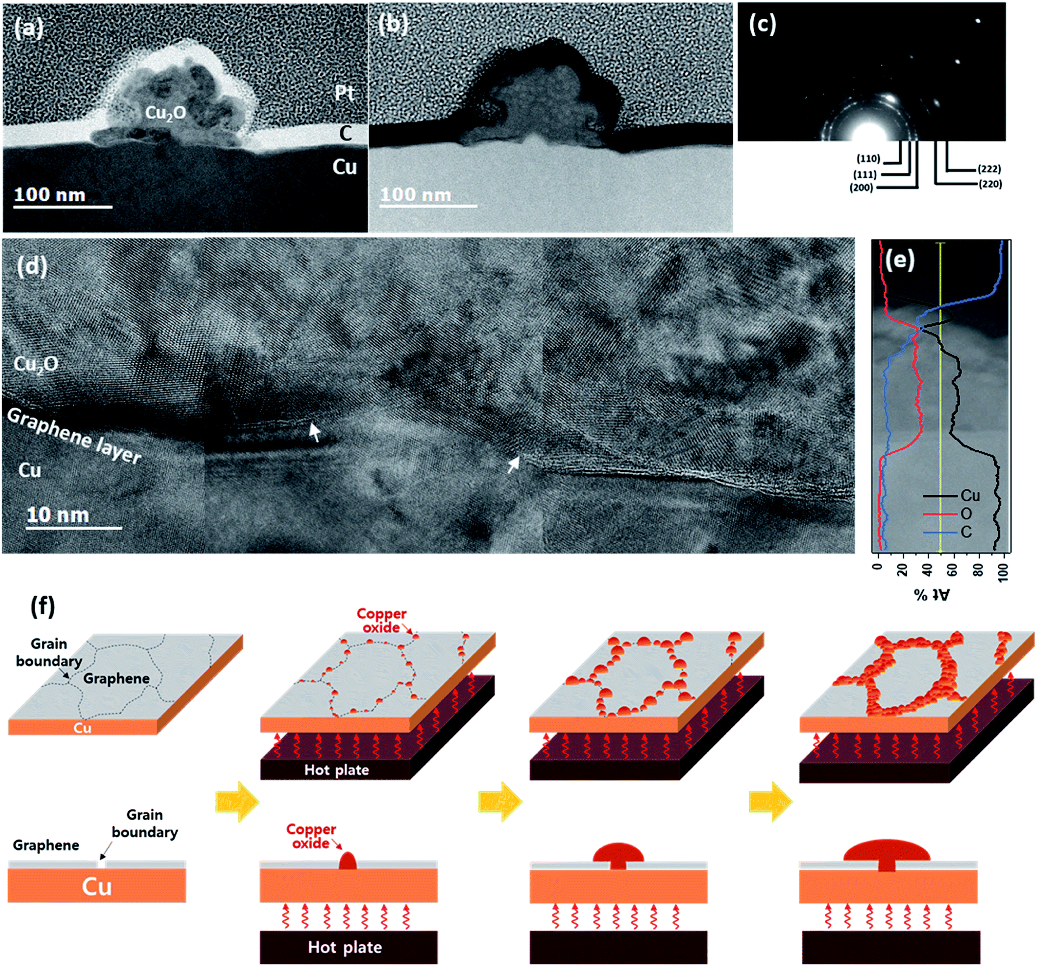 | ||
| Fig. 2 Cross-sectional TEM images and EDS analysis (a) bright-field STEM image, (b) HAADF STEM image, (c) SAED pattern of Cu2O, (d) HRTEM image, (e) EDS line spectrum across the interface between Cu and Cu2O, and (f) schematic diagrams of Cu oxidation through graphene grain boundary. | ||
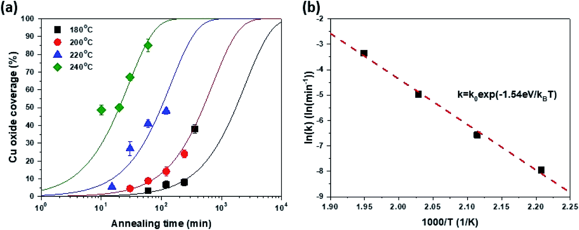 | ||
| Fig. 3 (a) Cu oxide coverage as a function of oxidation time and (b) oxidation reaction constant as a function of inverse oxidation temperature. | ||
The surface coverage of Cu2O (Fox) was assessed based on the OM images in Fig. 1. Here, the intensity of the OM image was normalized and the fraction of dark regions was estimated from the intensity histogram (for more details refer to ESI S-VI†). Fig. 3(a) shows the Fox as a function of tox and Tox. It is worth noting that the change in the Fox as a function of tox agrees well with the typical Johnson–Mehl–Avrami–Kolmogorov (JMAK) equation [eqn (1)] for predicting phase transformation kinetics based on nucleation and growth.36
| F = 1 − exp(−ktn), | (1) |
Furthermore, the k value related to the transformation rate was also extracted based on the JMAK equation in Fig. 3(a) and is plotted as a function of 1/Tox in Fig. 3(b). The slope of the curve fitted by the Arrhenius equation was 1.54 eV, which reflects the activation energy of Cu2O growth through graphene, representing the lateral growth rate of Cu2O. Therefore, the growth of Cu2O through graphene is controlled by Cu out-diffusion through Cu2O because this activation energy is similar to that of Cu diffusion in Cu oxide estimated in the classical Cu oxidation experiment.37 Consequently, it is possible to predict the kinetics of Cu oxidation through graphene at a certain targeting temperature through the JMAK equation using a k value obtained by extrapolation.
Electrical properties of graphene based on Cu oxidation
Previous results showed that Cu oxide grows on the graphene surface by out-diffusion of Cu ions through Cu oxide. To investigate the quality change in the graphene during Cu oxidation, the electrical properties of all samples were measured. All oxidized samples, as shown in Fig. 1, were transferred on a PET film; then, the Rs of graphene was examined by Hall measurement using the van der Pauw structure. The change in Rs as a function of tox at each Tox is illustrated in Fig. 4(a). At Tox of 180 °C, 200 °C, and 220 °C, the Rs values did not significantly increase compared to those of the as-grown graphene (Rs0 = 254 Ω sq−1) until 240, 120, and 15 min of oxidation, respectively. However, at Tox of 240 °C, Rs sharply increased after only 10 min of oxidation. To determine the cause of the change in Rs, ns and μ were measured as a function of tox by Hall measurement (Fig. 4(b) and (c)). Interestingly, ns maintains a value of 1.5 × 1013 cm−2, regardless of Tox and tox. However, there was a drastic change μ (Fig. 4(c)).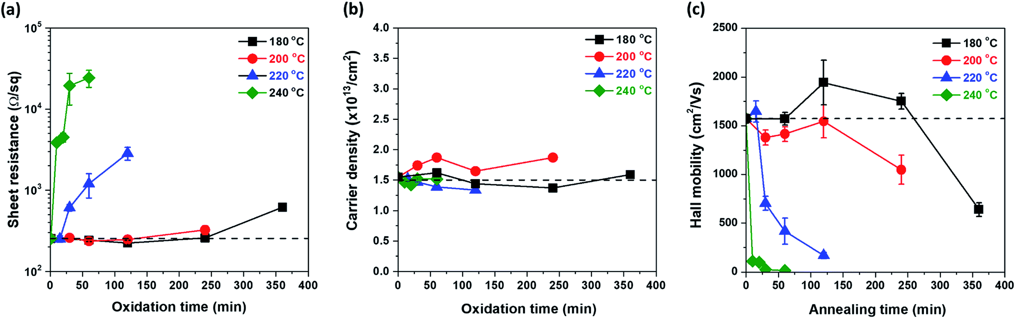 | ||
| Fig. 4 Electrical properties of graphene as a function of the oxidation time at different oxidation temperatures (180 °C, 200 °C, 220 °C, and 240 °C); (a) sheet resistance (b) sheet carrier density, and (c) Hall mobility with dashed lines which represent the values of the as-grown graphene. | ||
Because the electrical properties depend on both Tox and tox, it is difficult to quantitatively determine the effect of Cu oxidation on the electrical properties of graphene. Therefore, by expressing Tox and tox in terms of Fox, the electrical properties of graphene were plotted as a function of Fox (Fig. 5), in which the dashed lines represent the values of the as-grown graphene. As mentioned, ns was independent of Tox and tox and remained constant until Fox = 85% (Fig. 5(b)). The Rs and μ had different curves for each Tox, but these curves were merged into one curve by plotting it as a function of Fox. It clearly indicates that electrical properties of graphene are strongly related to Fox. From Rs = 1/nsqμ, the change in Rs as a function of Fox is fully described by the change of μ, inversely corresponding to the change of μ, because of the constant ns. The change in μ as a Fox is divided into three regions. In the first region (under Fox = 15%), the value of μ stayed at the as-grown value, and then the value of μ decreases linearly with the increase in Fox in the second region (Fox = 15–50%). Finally, the value of μ was only a few tens of cm2 V−1 s−1 over Fox = 50%. Herein, Cu2O is formed on the graphene surface and hence is undamaged by volume expansion (1.7 times) from Cu to Cu2O. However, as a defect site of the G-GB, the initial Cu2O nucleation site is the pathway of Cu cation out-diffusion (see the HRTEM image in Fig. 2(d)). The initial nucleation site is considered as a degraded G-GB point even before the Cu2O growth; thus, it may negligibly affect the electrical properties of graphene up to Fox = 15% of Cu2O growth. However, the continuous out-diffusion of Cu cations through the nucleation sites can expand and propagate the Cu cation diffusion path along with the G-GBs. When Fox exceeds 15%, the propagation of the Cu cation diffusion path becomes severe and μ of graphene is reduced. At Fox values above 50%, most of the graphene grains seem to be electrically disconnected. As electrical measurement inevitably involves charge carrier transfer, the mechanically weak points of the damaged grain boundaries can be further damaged during the transfer process, thereby exaggerating the decreasing tendency of the μ (see ESI S-VI†). From these results, we tried to provide optimal conditions for G-GB visualization through the contour map of Rs as a function of Tox and tox as shown in Fig. 5(d). The optimal condition requires a Fox enough to measure the graphene grain size at the same time without changing the electrical properties of graphene. Therefore, as mentioned above, the maximum value of Fox can be defined as 15%. On the other hand, G-GB is sufficiently revealed for measuring the graphene grain size when the amount of oxidation is at least about Fig. 1(b) and (f), and the Fox at this time is 10%. The boundary for optimal Fox values is shown as dashed lines in Fig. 5(d). The difference in oxidation time indicated by the distance between dashed lines at 200 °C is 50 min, so the process margin is very wide and oxidation time is relatively short which is compared to 180 °C. Therefore, oxidation at 200 °C for 100 min, can be suggested as an optimal condition for G-GB visualization.
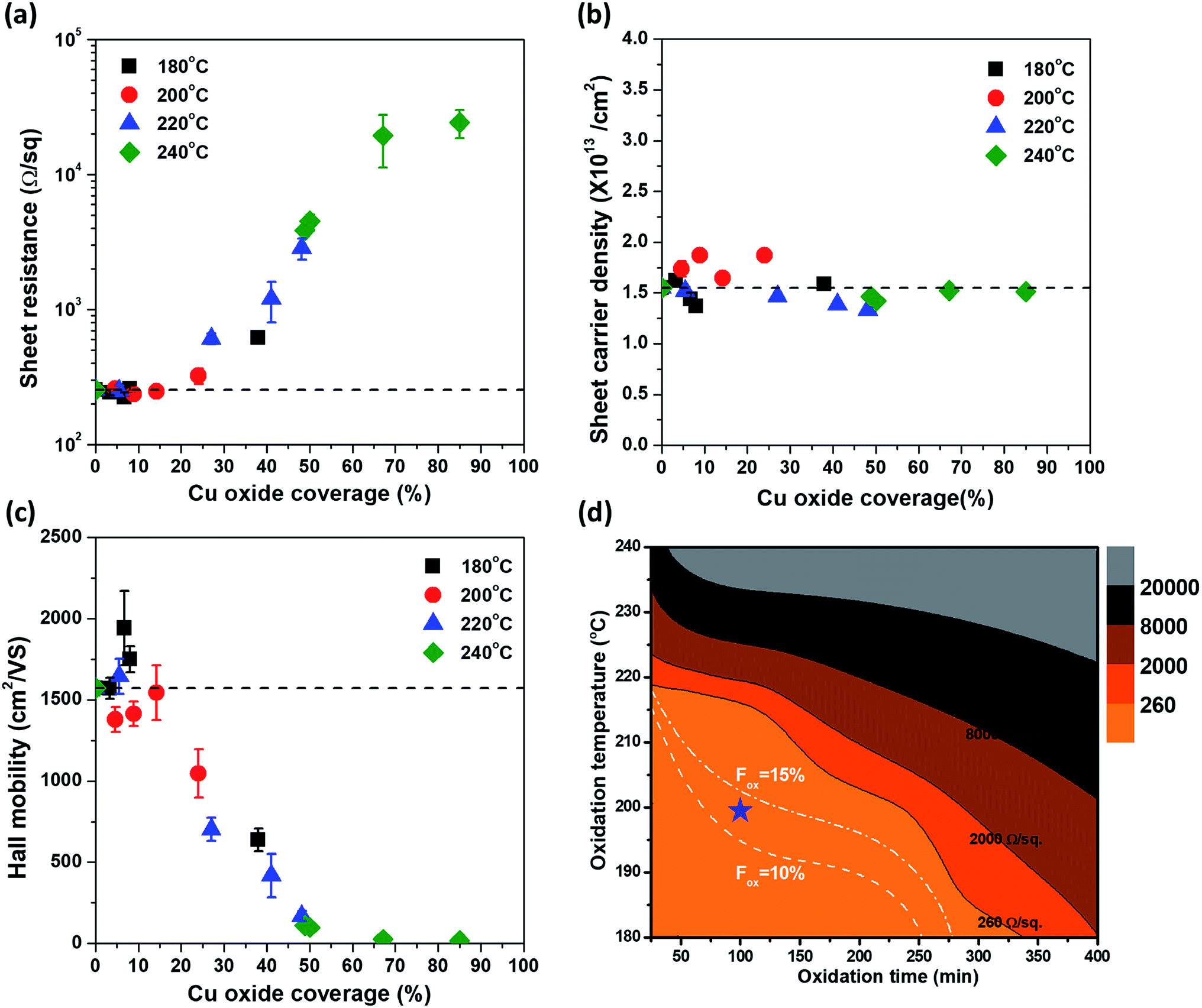 | ||
| Fig. 5 Electrical properties of graphene as a function of Cu oxide coverage at different oxidation temperature (180 °C, 200 °C, 220 °C, 240 °C); (a) sheet resistance, (b) sheet carrier density, and (c) Hall mobility. The black dashed lines represent the values of the as-grown graphene. (d) Contour map of graphene sheet resistance with white dashed lines which indicate constant Fox lines of 10% and 15%. The blue star represents the optimal condition of G-GB visualization. | ||
To explain the propagation of damage on G-GBs and electrical disconnection in the view point of Hall mobility variation as a function of Fox, the percolation probability was introduced in a simple schematic model of Cu oxidation at G-GBs. The percolation probability is used for conductivity prediction as a fraction of metallic component in composite materials.38 Because there is no mathematical formula for calculating the percolation probability, the percolation probability of graphene is simulated through a simple model, i.e., the graphene is disconnected as Cu oxide randomly nucleates and grows in G-GBs. The graphene grains in the 2D matrix were assumed to have square shapes to simplify the calculation (dashed line in Fig. 6(a)). Based on the morphological change illustrated in Fig. 1, we assumed the following steps. Step-I-nucleation, at the beginning, Cu oxide randomly nucleates at the G-GBs and there is no additional nucleation during the growth step (Fig. 6(b)). Step-II-oxygen impingement, the oxygen impingement is random (Fig. 6(c)). Step-III-Cu oxide growth, Cu oxide grows when the oxygen impinged near the already existing Cu oxide (Fig. 6(d)). After step-I-nucleation, step-II and step-III were repeated to grow Cu oxide. The random nucleation and continuous growth of Cu2O according to the iteration was provided in ESI S-VII† in the form of moving images. The connected graphene and Cu oxide coverage were estimated in each growth step using MATLAB software. The percolation probability, P(Fox), was 1 when the conducting path of graphene exists in both the x and y directions, 0.5 when the conducting path of graphene exists only in one direction (x or y), and 0 when the graphene is isolated by Cu oxidation. Fig. 6(e) and (f) show the graphene percolation probability and Cu oxide coverage, respectively, as a function of growth iteration. Each step function in Fig. 6(e) indicates 20 times repeated percolation probability with different initial positions of Cu oxide nucleus, and its average is shown as a gray solid curve. As shown in Fig. 6(f), the Cu oxide coverage increases with growth iteration, regardless of the initial position of the Cu oxide nucleus, whereas the graphene percolation probability is strongly affected by the initial position of the Cu oxide nucleus. Moreover, to investigate the effect of the amount of initial Cu oxide nucleus that might be related to G-GBs quality, the percolation probability was plotted as a function of the Cu oxide coverage [P(Fox)] by averaging 200 simulation units and varying the initial nucleus density (F_nc) from 20 to 200 ea/grain (as the solid lines in Fig. 6(g)). As oxidation progressed, there was a region where P(Fox) = 1 was maintained, after which P(Fox) decreased rapidly and eventually the conducting path of graphene disappeared [P(Fox) = 0]. P(Fox) = 1 reflects that the presence of the 2-directional conducting path in graphene and no disturbance to the charge transfer in the graphene. As P(Fox) < 1, the conducting path between graphene grains start to disappear, indicating the disturbance of the charge transfer in the graphene. The simulation results revealed that the Fox range at P(Fox) = 1 was determined by the initial nuclei density of Cu oxide at G-GB, which is related to the defect concentration in G-GB. This change in P(Fox) at F_nc = 40 ea per grain is very consistent with the change in the measured Hall mobility as shown in Fig. 6(h). Therefore, the relationship between the oxidized graphene morphology on Cu and its electrical properties was determined and the extent of morphological variation was assessed without affecting the graphene electrical properties. This simple modeling of Cu oxidation through graphene enables the calculation of the percolation probability of spanning graphene as a function of surface coverage of the Cu oxide, which is closely related to the carrier mobility within graphene.
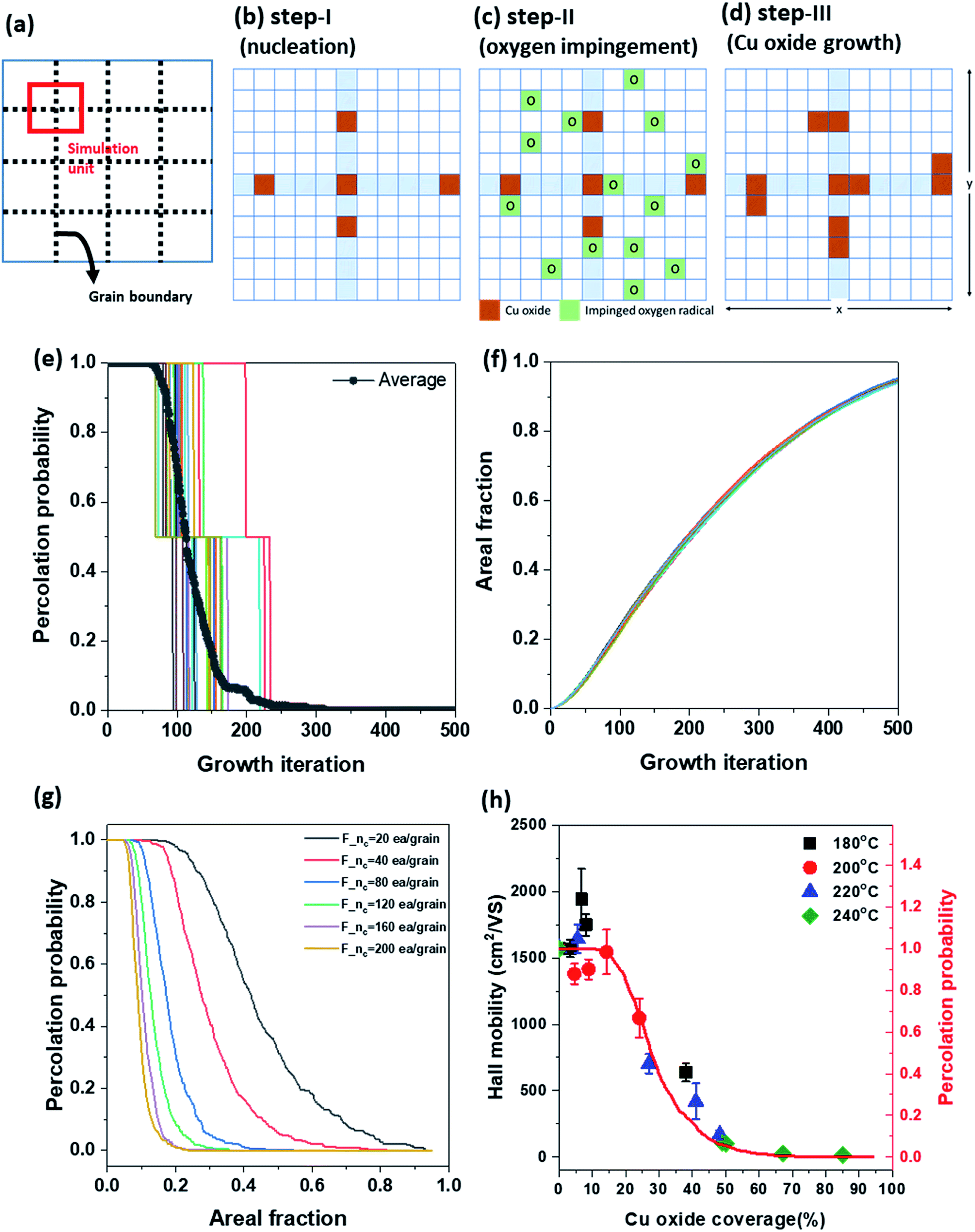 | ||
| Fig. 6 The relationship between Hall mobility and graphene percolation probability as a function of Cu oxide coverage: (a) schematics of the simulation unit and simulation step ((b) nucleation, (c) oxygen impingement, and (d) Cu oxide growth), (e) percolation probability and (f) areal fraction as a function of growth iteration, (g) percolation probability as a function of oxidation fraction, and (h) Hall mobility and percolation probability at F_nc = 40 ea per grain as a function of the oxidation fraction. | ||
Conclusion
Cu oxidation through graphene was investigated in detail as a function of temperature and time. The kinetics of Cu oxidation through graphene were quantitatively determined based on the Cu oxide coverage that was determined from the OM image. There are three 3 unique features in discussing Cu2O growth behavior on graphene. First, Cu2O growth kinetics undergoes one-dimensional growth. The OM image and JMAK equation analysis shows the Cu2O nucleation is limited in G-GBs and the Cu2O one-dimensionally grows with suppressed further nucleation. Second, the Cu2O growth is governed by dominant Cu cation out-diffusion in according to that; (i) HR-TEM analysis reveals graphene layer is at the Cu–Cu2O interface, (ii) the Cu oxidation predominantly occurs by dominant out-diffusion of Cu cation, (iii) the graphene layer is not critically damaged by the volume expansion of Cu oxide. Third, Fox of 10–15% confirmed that the graphene grain size could be measured without degradation of the electrical property of graphene, and suggested that the optimal condition considering practical points of experiments such as process margin is oxidation at 200 °C for 100 min. Also, the percolation probability could be predicted by simple modeling of Cu oxidation through graphene, the carrier mobility in graphene can also be estimated.Methods
Synthesis of graphene
The graphene was synthesized by RTCVD (NPS Corporation) on a 370 × 470 mm2 Cu foil (thickness: 0.35 mm, Nippon Mining & Metals Corporation). The Cu foil was loaded into a chamber and heated to 800 °C under CH4 atmosphere (30 sccm, 550 mTorr). The surface of Cu foil was then cleaned using pre-annealing, and the crystalline orientation of Cu was rearranged. Next, the graphene synthesis was performed by reheating the foil to 1025 °C for 1000 s. The chamber was cooled down to 600 °C and then to the room temperature by injecting CH4 and N2 gases, respectively.Cu oxidation on graphene/Cu foil structure
After the deposition, the graphene grown on Cu foil was cut into specimens of 3 × 3 cm2, and the samples were subjected to heat treatment on a hot plate for different durations at various temperatures under air atmosphere. Four different temperatures were chosen: 180 °C, 200 °C, 220 °C, and 240 °C. The oxidation time was varied from 10 to 360 min (Table 1).| Temperature (°C) | Oxidation time (min) | |||
|---|---|---|---|---|
| 180 | 60 | 120 | 240 | 360 |
| 200 | 30 | 60 | 120 | 240 |
| 220 | 15 | 30 | 60 | 120 |
| 240 | 10 | 20 | 30 | 60 |
Characterization of graphene and Cu oxide
After the oxidation of graphene on the Cu foil, surface images were acquired with OM (Olympus BX50). To identify the dark contrast of OM image, scanning electron microscope and Energy-dispersive X-ray spectroscopy (Merlin Compact, ZEISS) was conducted. The cross-sectional microstructure of graphene on Cu after oxidation was observed using Cs-corrected TEM (ARM 200F, JEOL Ltd.). The as-grown and heat-treated graphenes on Cu were transferred on a polymethyl methacrylate (PMMA) supporting layer in order to investigate the electrical properties of graphene. The PMMA was spin coated onto the graphene on Cu and then the underlying Cu was wet etched in imidazole-based Cu etchant (ammonium persulfate (0.1 M) + H2SO4 + H2O2). Thus, the graphene was simultaneously doped during the etching of Cu.29 The floated PMMA/graphene layer was scooped after 8 hours of complete Cu etching onto PET. Finally, the top PMMA layer was removed by acetone. The graphene electrical properties, i.e., sheet resistance, Hall mobility, and sheet carrier density, were measured by using a van der Pauw structure of 8 × 8 mm2. Hall measurements were performed under a 0.5 T magnetic field (HL 5500PC, BIO-RAD) at room temperature.Conflicts of interest
There are no conflicts to declare.Acknowledgements
This work was supported by the BioNano Health-Guard Research Center and funded by the Ministry of Science and ICT (MSIT) of Korea as a Global Frontier Project (2013M3A6B2078943) and the Nano Material Technology Development Program through the National Research Foundation of Korea (NRF) funded by the Ministry of Science and ICT (MSIT) of Korea (2015M3A7B4050454, 2015M3A7B4050452) and (2019R1A2C2005783).References
- K. S. Novoselov, A. K. Geim, S. V. Morozov, D. Jiang, Y. Zhang, S. V. Dubonos, I. V. Grigorieva and A. A. Firsov, Science, 2004, 306, 666–669 CrossRef CAS.
- X. S. Li, W. W. Cai, J. H. An, S. Kim, J. Nah, D. X. Yang, R. Piner, A. Velamakanni, I. Jung, E. Tutuc, S. K. Banerjee, L. Colombo and R. S. Ruoff, Science, 2009, 324, 1312–1314 CrossRef CAS.
- H. C. Lee, W. W. Liu, S. P. Chai, A. R. Mohamed, A. Aziz, C. S. Khe, N. M. S. Hidayah and U. Hashim, RSC Adv., 2017, 7, 28427 RSC.
- X. S. Li, C. W. Magnuson, A. Venugopal, R. M. Tromp, J. B. Hannon, E. M. Vogel, L. Colombo and R. S. Ruoff, J. Am. Chem. Soc., 2011, 133, 2816–2819 CrossRef CAS.
- Q. K. Yu, L. A. Jauregui, W. Wu, R. Colby, J. F. Tian, Z. H. Su, H. L. Cao, Z. H. Liu, D. Pandey, D. G. Wei, T. F. Chung, P. Peng, N. P. Guisinger, E. A. Stach, J. M. Bao, S. S. Pei and Y. P. Chen, Nat. Mater., 2011, 10, 443–449 CrossRef CAS.
- H. L. Zhou, W. J. Yu, L. X. Liu, R. Cheng, Y. Chen, X. Q. Huang, Y. Liu, Y. Wang, Y. Huang and X. F. Duan, Nat. Commun., 2013, 4, 2096 CrossRef.
- S. Y. Cho, M. S. Kim, M. Kim, K. J. Kim, H. M. Kim, D. J. Lee, S. H. Lee and K. B. Kim, Nanoscale, 2015, 7, 12820–12827 RSC.
- L. A. Jauregui, H. L. Cao, W. Wu, Q. K. Yu and Y. P. Chen, Solid State Commun., 2011, 151, 1100–1104 CrossRef CAS.
- G. Lopez-Polin, C. Gomez-Navarro, V. Parente, F. Guinea, M. I. Katsnelson, F. Perez-Murano and J. Gomez-Herrero, Nat. Phys., 2015, 11, 26–31 Search PubMed.
- F. Hao, D. N. Fang and Z. P. Xu, Appl. Phys. Lett., 2011, 99, 041901 CrossRef.
- Z. Yan, J. Lin, Z. W. Peng, Z. Z. Sun, Y. Zhu, L. Li, C. S. Xiang, E. L. Samuel, C. Kittrell and J. M. Tour, ACS Nano, 2012, 6, 9110–9117 CrossRef CAS.
- S. S. Chen, H. X. Ji, H. Chou, Q. Y. Li, H. Y. Li, J. W. Suk, R. Piner, L. Liao, W. W. Cai and R. S. Ruoff, Adv. Mater., 2013, 25, 2062–2065 CrossRef CAS.
- Y. F. Hao, M. S. Bharathi, L. Wang, Y. Y. Liu, H. Chen, S. Nie, X. H. Wang, H. Chou, C. Tan, B. Fallahazad, H. Ramanarayan, C. W. Magnuson, E. Tutuc, B. I. Yakobson, K. F. McCarty, Y. W. Zhang, P. Kim, J. Hone, L. Colombo and R. S. Ruoff, Science, 2013, 342, 720–723 CrossRef CAS.
- L. M. Malard, M. A. Pimenta, G. Dresselhaus and M. S. Dresselhaus, Phys. Rep., 2009, 473, 51–87 CrossRef CAS.
- A. C. Ferrari and D. M. Basko, Nat. Nanotechnol., 2013, 8, 235–246 CrossRef CAS.
- F. Tuinstra and J. L. Koenig, J. Chem. Phys., 1970, 53, 1126–1130 CrossRef CAS.
- A. Das, S. Pisana, B. Chakraborty, S. Piscanec, S. K. Saha, U. V. Waghmare, K. S. Novoselov, H. R. Krishnamurthy, A. K. Geim, A. C. Ferrari and A. K. Sood, Nat. Nanotechnol., 2008, 3, 210–215 CrossRef CAS.
- K. Kim, Z. Lee, W. Regan, C. Kisielowski, M. F. Crommie and A. Zettl, ACS Nano, 2011, 5, 2142–2146 CrossRef CAS.
- J. W. Suk, A. Kitt, C. W. Magnuson, Y. F. Hao, S. Ahmed, J. H. An, A. K. Swan, B. B. Goldberg and R. S. Ruoff, ACS Nano, 2011, 5, 6916–6924 CrossRef CAS.
- C. C. Jia, J. L. Jiang, L. Gan and X. F. Guo, Sci. Rep., 2012, 2, 707 CrossRef.
- J. Y. Lee, J. H. Lee, M. J. Kim, J. K. Dash, C. H. Lee, R. Joshi, S. Lee, J. Hone, A. Soon and G. H. Lee, Carbon, 2017, 115, 147–153 CrossRef CAS.
- K. P. Hong, D. Lee, J. B. Choi, Y. Kim and H. Kim, ACS Appl. Nano Mater., 2018, 1, 2515–2520 CrossRef CAS.
- D. L. Duong, G. H. Han, S. M. Lee, F. Gunes, E. S. Kim, S. T. Kim, H. Kim, Q. H. Ta, K. P. So, S. J. Yoon, S. J. Chae, Y. W. Jo, M. H. Park, S. H. Chae, S. C. Lim, J. Y. Choi and Y. H. Lee, Nature, 2012, 490, 235–239 CrossRef CAS.
- J. Kwak, Y. Jo, S. D. Park, N. Y. Kim, S. Y. Kim, H. J. Shin, Z. Lee, S. Y. Kim and S. Y. Kwon, Nat. Commun., 2017, 8, 1549 CrossRef.
- C. Kunka, S. Bavdekar, N. G. Rudawski, A. Fournier and G. Subhash, J. Phys. Mater., 2019, 2, 025005 CrossRef.
- T. Yoon, J. H. Mun, B. J. Cho and T. S. Kim, Nanoscale, 2014, 6, 151–156 RSC.
- S. S. Chen, L. Brown, M. Levendorf, W. W. Cai, S. Y. Ju, J. Edgeworth, X. S. Li, C. W. Magnuson, A. Velamakanni, R. D. Piner, J. Y. Kang, J. Park and R. S. Ruoff, ACS Nano, 2011, 5, 1321–1327 CrossRef CAS.
- J. M. Wofford, S. Nie, K. F. McCarty, N. C. Bartelt and O. D. Dubon, Nano Lett., 2010, 10, 4890–4896 CrossRef CAS.
- K. Jo, S. M. Kim, S. M. Lee, J. H. Kim, H. J. Lee, K. S. Kim, Y. D. Kwon and K. S. Kim, Carbon, 2015, 82, 168–175 CrossRef CAS.
- S. K. Lee, H. C. Hsu and W. H. Tuan, Mater. Res.-Ibero-Am. J., 2016, 19, 51–56 CAS.
- D. W. Bridges, J. P. Baur, G. S. Baur and W. M. Fassell, J. Electrochem. Soc., 1956, 103, 475–478 CrossRef CAS.
- S. Mrowec and A. Stoklosa, Oxid. Met., 1971, 3, 291–311 CrossRef CAS.
- L. P. Biro and P. Lambin, New J. Phys., 2013, 15, 035024 CrossRef.
- H. Jang, Z. H. Dai, K. H. Ha, S. K. Ameri and N. S. Lu, 2D Mater., 2020, 7, 014003 CrossRef.
- S. H. Bae, Y. Lee, B. K. Sharma, H. J. Lee, J. H. Kim and J. H. Ahn, Carbon, 2013, 51, 236–242 CrossRef CAS.
- M. Avrami, J. Chem. Phys., 1939, 7, 1103–1112 CrossRef CAS.
- Y. Ebisuzaki and W. B. Sanborn, J. Chem. Educ., 1985, 62, 341–343 CrossRef CAS.
- A. L. Efros and B. I. Shklovskii, Phys. Status Solidi B, 1976, 76, 475–485 CrossRef CAS.
Footnotes |
| † Electronic supplementary information (ESI) available. See DOI: 10.1039/d0ra06301k |
| ‡ These authors contributed equally to this work. |
| This journal is © The Royal Society of Chemistry 2020 |