
 Open Access Article
 This Open Access Article is licensed under a Creative Commons Attribution-Non Commercial 3.0 Unported Licence
Unveiling the optical parameters of vanadium dioxide in the phase transition region: a hybrid modeling approach†
Mehmet Cihan Cakir*ab,
Hasan Kocer *a,
Yilmaz Durnaf,
Deniz Umut Yildirimac,
Amir Ghobadiac,
Hodjat Hajiana,
Koray Ayding,
Hamza Kurtef,
Necdet Saglamb and
Ekmel Ozbay*acd
*a,
Yilmaz Durnaf,
Deniz Umut Yildirimac,
Amir Ghobadiac,
Hodjat Hajiana,
Koray Ayding,
Hamza Kurtef,
Necdet Saglamb and
Ekmel Ozbay*acd
aNANOTAM-Nanotechnology Research Center, Bilkent University, 06800 Ankara, Turkey. E-mail: ccakir@bilkent.edu.tr; hasan.kocer@bilkent.edu.tr; ozbay@bilkent.edu.tr
bDepartment of Nanotechnology and Nanomedicine, Hacettepe University, 06800 Ankara, Turkey
cDepartment of Electrical and Electronics Engineering, Bilkent University, 06800 Ankara, Turkey
dDepartment of Physics, Bilkent University, 06800 Ankara, Turkey
eDepartment of Electrical and Electronics Engineering, TOBB University of Economics and Technology, 06560 Ankara, Turkey
fNanophotonics Research Laboratory, TOBB University of Economics and Technology, 06560 Ankara, Turkey
gDepartment of Electrical Engineering and Computer Science, Northwestern University, 60208 Evanston, Illinois, USA
First published on 13th August 2020
Abstract
The phase change behavior of vanadium dioxide (VO2) has been widely explored in a variety of optical and photonic applications. Commonly, its optical parameters have been studied in two extreme regimes: hot (metallic) and cold (insulating) states. However, in the transition temperatures, VO2 acts like an inherent metamaterial with mixed metallic-insulating character. In this range, the portions of metallic and insulating inclusions are tuned by temperature, and therefore a gradual change of optical parameters can be achieved. In this paper, a universal hybrid modeling approach is developed to model VO2 in the intermediate region. For this aim, the measured reflectivity data, is analyzed and matched through the transfer matrix method (TMM) simulations where an effective medium theory (EMT) is employed. Based on the findings of this approach, not only the relative portions of inclusions are tailored but also their grain shapes are significantly altered in the transition range. Finally, the modeling approach is testified by experimental findings through dynamic device applications operating at short and mid infrared wavelengths. In addition, the hysteretic behaviors on electrical, optical, and structural parameters of the VO2 film along the heating and cooling cycles are demonstrated by the experiments and scrutinized by the simulations.
Introduction
Vanadium dioxide (VO2) is an exotic material in which its phase changes from an insulator to a metal after a conveniently accessible transition temperature (∼68 °C).1 This phase transition is reversible, that is, when it reduces from higher temperatures to lower temperatures, the phase transition from metal to insulator occurs. For this reason, it has been the most attractive material among the phase change materials since its discovery in 1959.2 The material, having the insulating phase at room temperature and metallic phase at high temperature, would be in an intermediate phase when approaching the transition point either from higher or lower temperatures. In other words, VO2 is an inherent metamaterial in atomic scales. The phase transition of the VO2 can be triggered thermally,3–6 electrically,7–9 optically,10 and mechanically.11 The electrical and optical properties of the VO2 before, during, and after the phase transition differ considerably in the spectra of interest. Many applications have been developed from radio frequency (RF) to optical spectrum, employing this phase transition character. Some of these applications are infrared (IR) camouflage,12–14 smart thermochromic coatings,15,16 IR sensors,17,18 optical diode-like structures,19,20 optical metasurfaces,21,22 switching,23,24 and terahertz devices.25,26 The electrical and spectral optical properties of the VO2 depend on the quality of the VO2 film, i.e. the type of growth, growth conditions, substrate type, etc.27,28 Thin VO2 films can be grown on different substrates by various techniques. The main growth techniques are sol–gel deposition,15,29–31 sputtering,32–35 pulsed laser deposition (PLD),36–39 chemical vapor deposition (CVD),40–44 and reactive evaporation.45 Some widespread substrates employed for VO2 growth are sapphire (Al2O3),46 titanium dioxide,47 silicon,48 germanium,49 and gallium nitride.50 In addition, VO2 thin film growth on graphene51 and hexagonal boron nitride (hBN),52 which are transferable to flexible substrates, were reported. The diversity of VO2 growth and applications calls for a detailed knowledge on the optical parameters of VO2 at relevant operating temperatures and the wavelengths. Although many reports3–6,19,51 have extracted the refractive index of VO2 in hot or metal (m-VO2) and cold or insulator (i-VO2) states, its optical behavior in the transition region has not been scrutinized. This is the regime in which material itself operates as a metamaterial. To our knowledge, there has not been much comprehensive study on the spectral optical parameter extraction of VO2 depending on the temperature and specific to VO2 growth conditions, except for one recent study.53This paper shows a comprehensive study of extracting optical parameters in all phase transition regimes of VO2 starting from a bare film and eventually to a device application in the short-wavelength infrared (SWIR) and mid-wavelength infrared (MWIR) spectra. The spectral optical parameters of the VO2 at each temperature during the heating and cooling cycles are modeled utilizing an effective medium theory (EMT) approach in the electromagnetic simulations. Thanks to fine adjustments of parameters in the EMT modeling, spectral measurements and simulations are matched at every specific temperature. In this way, the size and shape changes in the metallization regions inside an ultrathin (∼90 nm thick) grown VO2 film, which take place on an atomic scale during phase transition, are discovered by extensive experiments and simulations, based on the applied temperature intensity and direction. Our method concludes that the volume of metalized VO2 regions is directly proportional to the applied temperature as expected. However, the most notable observation of this modeling approach is its prediction on optical behavior of VO2 film in the phase transition regime. For the first time, our study reveals that the shape of metallic inclusions in the VO2 layer differs only in the transition region compared to other regimes. In addition, the hysteretic behaviors, occurring in various parameters during the heating and cooling processes, are explored by the experiments and simulations. Finally, as a proof-of concept study, we design a tunable device, using the extracted optical parameters, and we theoretically and experimentally demonstrate its operation in the SWIR and MWIR wavelengths. Moreover, we make additional numerical simulations of the final device to enlighten the physics behind the operating mechanism, and its angular and the polarization dependency. While most of the previously reported studies concentrated on the optical character of VO2 in only hot and cold states, accurate modeling of the material behavior in the intermediate transition region can be used to design multi-functional linearly tunable optical systems.
Materials and methods
Growth of VO2 thin films
RF magnetron sputtering technique was used to deposit VO2 thin film on double side polished c-plane sapphire substrate. A vanadium oxide target was used as the source material. Deposition pressure was 2.4 × 10⁻³ mbar and argon (Ar) flow was 7 sccm. Deposition rate was ∼0.4 Å s−1. The thickness of deposited VO2 film was 90 nm. Post annealing was done at 400 °C for 1 hour in atmospheric tube furnace under Ar flow of 4 cm3 min−1. The sapphire substrate was selected for its superior transmittance up to 6 μm mid infrared wavelengths.Fabrication of the samples
Following the growth and annealing of VO2 on the sapphire substrate, three 5 × 5 mm samples were diced for the fabrication of samples A, B, and C. The bare film referred as “sample A” was used for temperature dependent electrical and FTIR reflectivity measurements of the grown VO2. “Sample B” was prepared depositing 100 nm of gold (Au) on one of diced VO2 samples by electron-beam evaporation system. The chamber pressure was 1 × 10⁻⁵ mbar while the deposition rate was 2 Å s−1. For the fabrication of “sample C”, firstly 520 nm of SiO2 was deposited on the VO2 by plasma-enhanced chemical vapor deposition (PECVD). The PECVD temperature was 250 °C and the process pressure was 80 Pa with 300 sccm N2O flow rate while the RF power was 50 W. After the SiO2 deposition, 100 nm Au was deposited by electron-beam evaporation with the same process parameters described for “sample B”.Electrical measurements
4-Probe sheet resistance technique utilizing Agilent B1500A Semiconductor Parameter Analyzer was performed to measure the dc electrical sheet resistance of “sample A” while changing the temperature from 25 °C to 90 °C and back down. During these temperature cycles, we chose a relatively fine resolution of 2 °C in the expected material phase transition region, and a resolution of 5 °C elsewhere. A thermoelectric cooling (TEC) chuck was used as the heating stage. A 10 A/12 V TEC controller (Arroyo Instruments 5310) was operated to control the temperature. At each temperature measurement, we waited at least 60 seconds for the temperature to settle.Optical measurements
The infrared spectral reflectivity measurements of the samples were carried out using an IR microscope (Bruker Hyperion 2000) and the Fourier transform infrared (FTIR) spectrometer (Bruker Vertex 70v) with a liquid nitrogen cooled mercury cadmium telluride detector and mid-IR source. Reflected light was collected with a 15× magnification reflective objective (numerical aperture 0.4). To calibrate, a thick gold layer coated on sapphire substrate was used as the background in the reflection measurement. In order to change the temperature from the room temperature (T = 25 °C) to the high temperature (T = 90 °C) during the heating and from T = 90 °C to T = 25 °C during the cooling, the samples were placed on a heating stage that is mounted on the IR microscope, with a temperature controller (Arrayo TEC). After adjusting the controller of the heating stage, we waited at least 60 seconds to let the sample arrive to the desired temperature.Simulations
In the Transfer Matrix Method (TMM), the field within each layer could be treated as superposition of forward-traveling (transmitted) and backward-traveling (reflected) wave with a wave number k and a transfer matrix could represent the propagation through interface or within medium. By cascading the transfer matrix for each layer, the entire system transfer matrix can be obtained, deriving the spectral transmittance (T) and spectral reflectivity (R) of the structure.54 The mathematical details of these derivations and the incidence angle and the polarization modeling using TMM were given by Kocer et al.55 The absorbed power and electric field intensity distributions along “sample C” were computed via finite-difference time-domain (FDTD) simulations with a commercial software from Lumerical Solutions.56 While a TM polarized plane wave of 4 μm was sent at normal incidence in the FDTD simulations, periodic boundary conditions were applied along transverse axes perpendicular to the light propagation axis, and PML (perfectly matched layers) boundary conditions were selected along the propagation axis. Then, the electric field and absorbed power distributions were determined within the frequency profile and power monitors.Results and discussion
The fabrication of the bare film (referred as “sample A”) involves growing of a 90 nm VO2 layer on the c-plane sapphire by RF magnetron sputtering. Then, we place it in a temperature controlled stage to make electrical resistance measurements as shown in the inset of Fig. 1a. Utilizing the 4-probe sheet resistance technique, we measure the dc electrical sheet resistance of the “sample A” while changing the temperature from 25 °C to 90 °C and back down (during heating step size of 2 °C in the range of 60–80 °C and 5 °C outside of this range, and during the cooling step size of 2 °C in the range of 50–80 °C and 5 °C outside of this range). In each temperature measurement during the heating and cooling cycles, we wait at least 60 s to allow the temperature to settle. Fig. 1a exhibits the mentioned measurement results as the normalized dc sheet resistance Rsh(T)/Rsh(25 °C). It shows more than four orders of magnitude change between cold (T = 25 °C) and hot (T = 90 °C) states. In addition, when we compare the blue (during cooling) and red (during heating) curves in the Fig. 1a, it is seen that the normalized dc sheet resistance shows a hysteretic behavior, which is elucidated later. It is also evident that the transition of the resistance in our sample across the phase transition region is steeper (during cooling: 0.95 decade per °C and during heating: 0.64 decade per °C) when we compare it with a similar structure57 in the literature. Overall, the electrical measurements prove that our growth method achieves an appropriate VO2 material that can change its phase in a reversible manner, by switching from the insulating state to the conductive state with a rather steep slope according to the temperature shift. In order to visualize the structural morphology and uniformity of the VO2 film, the scanning electron microscope (SEM) image of the top surface of the “sample A” is obtained in Fig. 1b. The inset is the optical image of the top of the real sample next to a coin as well. The SEM image reveals that the surface morphology of the VO2 film seems to be continuous with multi domains due to the magnetron sputtering. To assess the surface roughness of the VO2 film, we use atomic force microscopy (AFM) measurement on the top surface of the “sample A”. The resulting 2D and 3D AFM images are seen in Fig. 1c and d, respectively. According to AFM imaging, the average surface roughness (Ra) is found to be 7.7 ± 0.8 nm. This value of Ra is much smaller than the wavelengths (λ ≥ 1 μm) in our study. Therefore, in the simulations at these wavelengths, we can treat the top of the VO2 film as if it was smooth.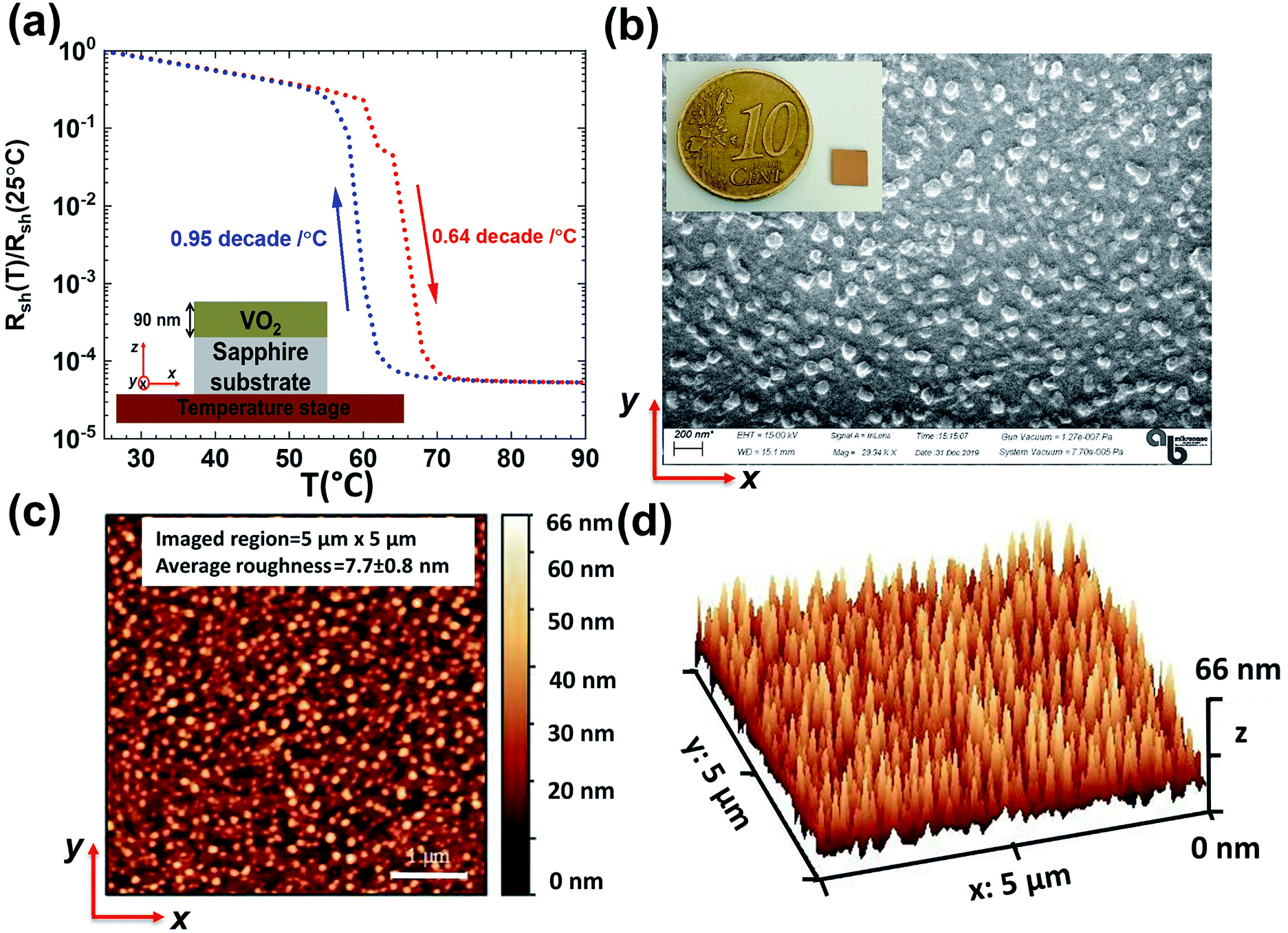 | ||
| Fig. 1 (a) Electrical characterization of VO2 ultrathin film (“sample A”) as a function of temperature during heating (red colored) and cooling (blue colored). The inset depicts the x–z side view of the “sample A” on a temperature stage. (b) Scanning electron microscope image of the “sample A”. Inset: Optical image of the “sample A” and size comparison with a coin of 10 eurocents. (c) 2D and (d) 3D atomic force microscopy images of the “sample A”. | ||
After the electrical and surface characterizations of “sample A”, we start IR spectral reflectivity measurements using an IR microscope (Bruker Hyperion 2000) that is coupled to the Fourier transform infrared (FTIR) spectrometer (Bruker Vertex 70v). As seen in the inset of Fig. 2a, “sample A” is placed on a temperature controlled stage that is mounted inside the IR microscope/FTIR. The sample is exposed to near normal incidence of the IR light at wavelengths of 1 to 15 μm. In the heating step, the temperature increases from 25 °C to 90 °C and vice versa in the cooling process. As can be seen in the temperature values shown in the lower right side of Fig. 2, which we use in the heating and cooling phases, the reflectivity measurements RFTIR(T,λ) are made between 55 °C and 70 °C in one degree steps. Since VO2 material phase transition is between 55 °C and 70 °C, the reflectivity measurements in this range are done in fine steps compared to the other ranges. An optically thick gold mirror is used for the normalization in the reflectivity measurements. In addition, we perform the FTIR measurements during the cooling and the heating after staying at least 60 s at each temperature to sense the set temperature correctly. As a result, the spectral plots for the RFTIR(T,λ) are given in Fig. 2b (during heating) and Fig. 2e (during cooling). The small resonating features at 4.2 μm are due to absorption of the atmospheric CO2 molecules, which exist in the measurement environment. Considering the RFTIR(T,λ) spectra during the heating (the cooling), we observe that these reflectivities do not switch monotonously from low (high) to high (low) temperatures. These characteristics stem from the complicated interaction between the effective medium formed when VO2 is in an intermediate material state during these temperature transitions and the underlying sapphire substrate. In both of the spectra in the heating (Fig. 2b) and the cooling (Fig. 2e) periods, this situation can be especially viewed at 11.3 μm wavelength. Namely, when the material state of the VO2 is an insulator at the room temperature (T = 25 °C) and a metal at the elevated temperature (T = 90 °C), the reflectivity values, which are quite high, are approaching zero suddenly at the intermediate temperatures. Furthermore, the sapphire substrate is not transmitting at this wavelength, but highly reflective. Therefore, the sudden drop of the reflectance at this particular wavelength at a certain temperature can be attributed to the absorption inside the VO2 layer, which turns to the intermediate material state or inherent metamaterial. In addition, the reflectivity spectrum at 11.3 μm wavelength has a hysteresis, which is discussed later in the text. Since the VO2 exhibits such a complex optical behavior related to the temperature changes, it is important to reveal the spectral optical parameters of the VO2 depending on the temperature values in the case of temperature rise or decrease.
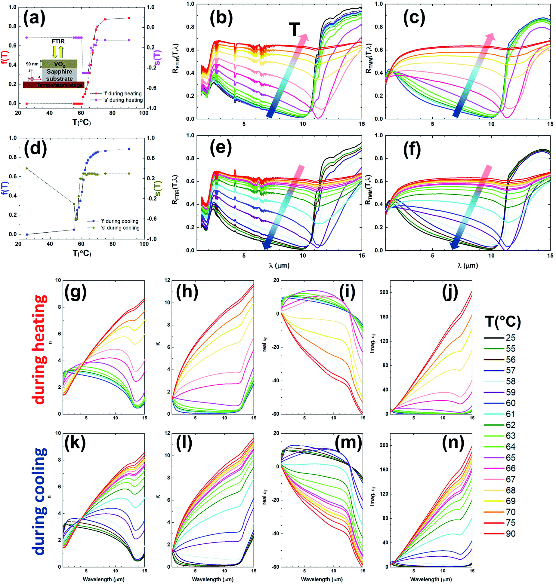 | ||
| Fig. 2 During heating: (a) Looyenga effective-medium theory parameters of f(T) and s(T), (b) measured spectral reflectivity of RFTIR(T,λ) and (c) simulated spectral reflectivity of RTMM(T,λ). Inset (a) is x–z side view of the “sample A” on a temperature stage. During cooling: (d) Looyenga effective-medium theory parameters of f(T) and s(T), (e) measured spectral reflectivity of RFTIR(T,λ) and (f) simulated spectral reflectivity of RTMM(T,λ). Extracted infrared spectral optical parameters of VO2 in “sample A” during heating: (g) real and (h) imaginary parts of the refractive indices, and (i) real and (j) imaginary parts of relative dielectric permittivities. Extracted infrared spectral optical parameters of VO2 in “sample A” during cooling: (k) real and (l) imaginary parts of the refractive indices, and (m) real and (n) imaginary parts of relative dielectric permittivities. The colored horizontal lines on the right refer to the temperatures applied during heating and cooling. | ||
VO2 at and near the phase transition behaves like a natural metamaterial that contains metallic and insulating inclusions that are much smaller than the wavelength of the incident light. In addition, the sizes of the metallic and insulating domains vary depending on the temperature. As the temperature increases, the volume occupied by the metallic domains increases, while the one for the insulating domains decreases, and the opposite occurs when the temperature decreases. Therefore, the spectral optical parameters of VO2 at different temperatures can be better assessed by an appropriate EMT. In our study, we implement a method utilizing an EMT. This method is based on the theoretical convergence to the reflectivity values obtained experimentally by performing the electromagnetic simulations of the “sample A” with Transfer Matrix Method (TMM)54,55 as follows.
| RTMM(T,λ,εeff(T,λ)) ≈ RFTIR(T,λ) | (1) |
The key parameter in eqn (1) is the εeff(T,λ) that represents the effective complex relative dielectric permittivity of the VO2 layer in the “sample A”. Although there are many EMT models developed in the past to deal with the intermediate states of VO2, we use EMT based on the Looyenga mixing rule,53,58 as it has the more versatile modeling capabilities described below.
| εs(T)eff(T,λ) = (1 − f(T))εs(T)ins(λ) + f(T)εs(T)met(λ) | (2) |
Following the agreement between FTIR and TMM spectral reflection through f(T) and s(T) adjustments, we can extract the temperature dependent spectral optical parameters of the VO2 presented in Fig. 2g–n. For this purpose, we apply a systematic approach. At first, we calculate the temperature dependent real and imaginary components of the spectral optical parameters of the VO2 in the heating phase by placing the parameters we identified in Fig. 2a in eqn (2). In this manner, the real part of the refractive index, n(T,λ), the imaginary part of the refractive index, K(T,λ), the real part of the relative dielectric permittivity, real εeff(T,λ), and the imaginary part of the relative dielectric permittivity, imag. εeff(T,λ), are given in Fig. 2g, h, i, and j, respectively. Next, when we insert the data from Fig. 2d in eqn (2), the mentioned optical parameters in the heating phase are now calculated for the cooling phase, and the results are presented in Fig. 2k–n, respectively. The aforementioned parameters are illustrated as 2D maps during heating and cooling in the ESI (Fig. S2 and S3†). Here, the important contour lines such as n(T,λ) = 1 (close to air) and real εeff(T,λ) = 0 (epsilon near-zero, ENZ) are shown separately for the heating and cooling conditions, and their behaviors are explained comparatively.
For the “sample A” in the inset of Fig. 3a, the hysteretic behaviors we encounter during the electrical/optical measurements and the optical simulations are exhibited collectively in Fig. 3. For all of the figure of merits whose hystereses are plotted here, the red colored data reflects the heating and the blue colored ones reflect the cooling state. Fig. 3a implies that the normalized dc sheet resistance has a hysteresis width of about 7 °C between the linearly sloping curves of 0.95 decade per °C and 0.64 decade per °C. This hysteresis width is close to the findings of an experimental study57 similar to our growth conditions except the VO2 thickness was two times of the ours. Fig. 3b shows another hysteresis we experienced. During the cooling and heating, the difference between the reflectivity drops occurring at the wavelength of 11.3 μm is found as ∼7 °C by means of compatible FTIR measurements and TMM simulations. In addition, when full width at half maximum (FWHM) values are quantitatively compared with the experiments and the simulations in the cooling and the heating phases, it is seen that they are not very different from each other as given inside the Fig. 3b. The last hysteretic behaviors are indicated in the EMT parameters of f(T) and s(T) in Fig. 3c and d, respectively. Comparing the red and the blue colored data in terms of the hysteresis, we observe that maximum width across the linear region in f(T) and the difference between the dips of the valleys in s(T) are ∼7 °C. Furthermore, the additional hystereses of the optical parameters at some selected wavelengths are also illustrated in the ESI (Fig. S4†). After all, the common feature of the four different hystereses in the main text and four in the ESI† is that they are all of the same value (i.e. ∼7 °C). Although the hysteretic behaviors with the same value are rarely seen in one or two parameters of VO2 in the literature,57 the hysteretic behaviors with the same value in more than two different parameters are disclosed for the first time in this study.
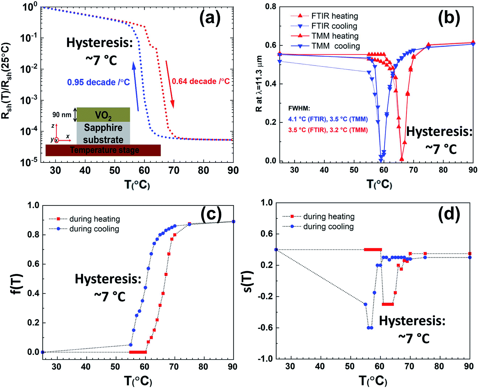 | ||
| Fig. 3 Hysteretic behaviors observed in (a) normalized electrical resistance, (b) experimental (FTIR) and simulated (TMM) reflectivity (R) from the “sample A” at λ = 11.3 μm, effective-medium theory parameters of (c) f(T) and (d) s(T) as the applied temperature increases and decreases. Inset (a) is x–z side view of “sample A” on a temperature stage. | ||
After implementing the proposed optical parameter extraction, a proof-of-concept study is carried out to demonstrate a device application using the optical parameters of the VO2 film, which we have revealed as a result of the experimental and the theoretical studies of the material and optical properties described above in detail. Our goal is to design and experimentally show a tunable device60 at SWIR and MWIR wavelengths using “sample A” and its optical parameters. We also employ a planar and lithography-free device architecture to benefit the ease of the fabrication.61 We will follow a three-step theoretical and experimental process toward the specified goal. Firstly, shown in Fig. 4a (left inset), we illuminate “sample A” from the sapphire side at the normal incidence in SWIR and MWIR wavelengths and perform the FTIR measurements and the TMM simulations under the conditions of T = 25 °C and T = 90 °C. Since the sapphire is highly transmissive and lossless in our wavelength range (1 μm ≤ λ ≤ 6 μm), we set its refractive index as 1.70 in the simulations.3,4 Utilizing the spectral optical data of the VO2 that we have already extracted in the Fig. 2, we pick the optical parameters at T = 25 °C where the VO2 is an insulator (i-VO2) and T = 90 °C where the VO2 is a metal (m-VO2). When we compare the measured and simulated spectral reflections in Fig. 4a, it is seen that the experiments and simulations are compatible and there is a certain contrast between the reflection spectra in two different temperature conditions. This contrast can be easily explained with the field intensity in the VO2, I(T,λ,z). It decays as I(T,λ,z) ∼ exp{−z/δ(T,λ)}. δ(T,λ) is the skin depth and expressed as δ(T,λ) = λ/4πK(T,λ), which is dependent on the wavelength and the imaginary part of the refractive index of the VO2. Taking the K(T,λ) from Fig. 2 at T = 25 °C and T = 90 °C, we calculate the spectral skin depth at these temperatures in the right inset of the Fig. 4a. Since the δ(T = 25 °C,λ) is much higher than the thickness of the VO2, the incoming IR light can pass through the i-VO2 layer with higher transmission, lower reflection, and negligible absorption, whereas the opposite situation occurs at T = 90 °C. Namely, the transmission decreases and the absorption and reflection increase due to the δ(T = 90 °C,λ), which is smaller than the VO2 thickness. According to the well-known conservation of the power, the sum of reflection (R), transmission (T), and absorption (A) ratios is fixed as R + T + A = 1. If we block the transmission completely, it is reduced to A + R = 1. The second step of our study is now targeted toward this purpose such that we coat an optically thick gold (Au) layer (∼100 nm) on the VO2 side displayed in the inset of the Fig. 4b as “sample B”. In this case, the transmission will no longer occur. Here and the later simulations, we select “Au (gold)-CRC” as the Au's spectral refractive index from the material library of Lumerical, a commercially available finite-difference time-domain (FDTD) simulation software package.56 As seen in Fig. 4b, the simulated and measured reflectivity contrast reverses compared to “sample A”. At T = 25 °C, the IR illumination at λ > 2 μm can pass through the i-VO2 without much loss, hitting the thick Au layer and almost the majority is reflected back. At T = 90 °C, the same illumination is absorbed more in the transitions from the lossy m-VO2, so the reflection is relatively reduced compared to the previous situation. Although we have a fairly good agreement between the simulations and the measurements to estimate the reflection contrast, it is necessary to explain the deviation observed between them. This might primarily have been originated from the fact that the refractive index of the experimental 90 nm thick Au structure might be somewhat different than the bulk index of the “Au (gold)-CRC”. Secondly, the experimental sapphire index may exhibit slightly dispersive and lossy characteristics instead of the constant one, which was not considered in our simulations. In order to further rise this reflection contrast, we incorporate a SiO2 spacer layer between VO2 and Au as the last step. We investigate the effect of the thickness of this spacer layer via numerical simulations in Fig. 4c at T = 25 °C and T = 90 °C separately. To accurately simulate the device response, we measure the spectral refractive index of the SiO2 film using variable angle spectroscopic ellipsometer in the ESI (Fig. S5†). Then, we fabricate the structure (“sample C”) with the 520 nm thick SiO2 layer as seen in the inset of Fig. 4d. In Fig. 4d, we finally achieve broadband and tunable reflection at SWIR and MWIR wavelengths through the experiments and simulations that give quite close results. Some minor discrepancies that do not affect our main purpose are caused by the aforementioned reasons, and unavoidable imperfections during the fabrication and measurements. Moreover, we enlighten the physics behind this exclusive operating mechanism by the additional electromagnetic simulations given in the ESI (Fig. S6–S8†). To assess the angular and the polarization dependency of the proposed device, TMM simulations are carried out for four different illumination and temperature conditions, which are depicted as insets in Fig. 5. In “TE” or “s” polarization, the electric field is normal to the incidence (x–z) plane, whereas it is inside the incidence plane in “TM” or “p” polarization. The angle of incidence varies in all cases from 0° to 80° in 10° steps. In Fig. 5, the sub-items in each row show the effect of polarization at a constant temperature, while those in each column are the effect of the material state at constant polarization. We can elucidate the comments about these findings as follows. First, the desired device performance can be achieved in TM polarization (Fig. 5b and d) up to higher incidence angles compared to TE polarization (Fig. 5a and c). Secondly, it is also possible to say that the device performance up to 50° of incidence is almost maintained for both polarization conditions. Therefore, it would not be wrong to claim that our design is considerably independent in terms of the polarization and the angle of incidence.
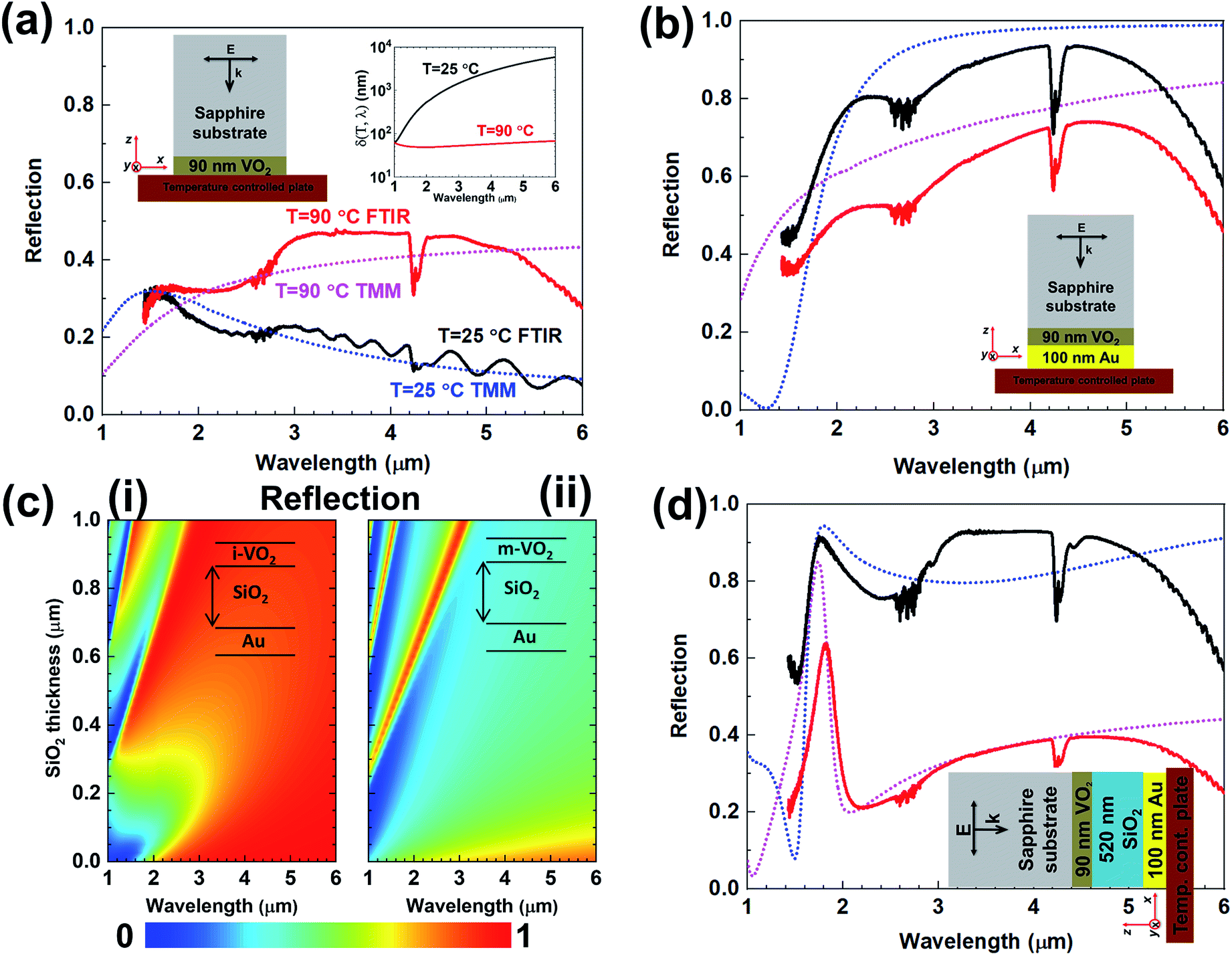 | ||
| Fig. 4 (a) Simulated (TMM) and measured (FTIR) power reflection spectra of the structure shown in left inset (“sample A”) at T = 25 °C and T = 90 °C. Right inset: the spectral skin depth of VO2 at T = 25 °C and T = 90 °C, (b) TMM and FTIR reflection spectra of the structure shown in inset (“sample B”) at T = 25 °C and T = 90 °C, (c) reflection map with respect to the thickness of SiO2 layer (which is added between VO2 and Au layers of “sample B”) (i) at T = 25 °C and (ii) at T = 90 °C. The bottom color bar applies both. (d) TMM and FTIR reflection spectra of the structure shown in inset (“sample C”) at T = 25 °C and T = 90 °C. Solid red (T = 90 °C) and black (T = 25 °C) curves represent FTIR power reflections, whereas dotted pink (T = 90 °C) and blue (T = 25 °C) curves represent TMM power reflections in (a), (b) and (d). | ||
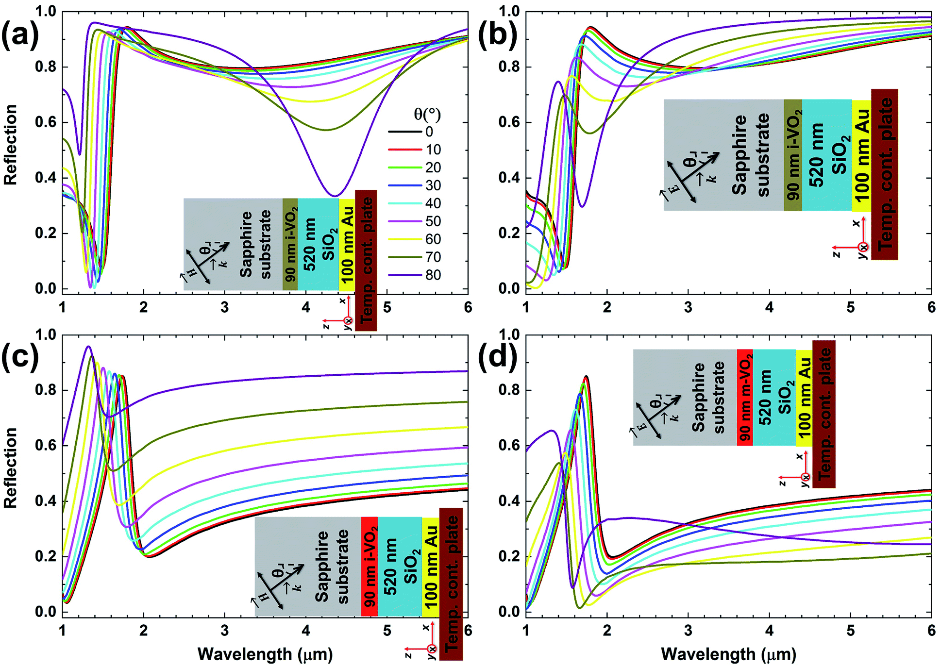 | ||
| Fig. 5 The angular dependence of infrared reflection when VO2 is insulator under (a) TE and (b) TM polarized illuminations and when VO2 is metallic under (c) TE and (d) TM polarized illuminations. The x–z side views of the simulated geometries and illumination conditions are pictured in the insets. The horizontal colored lines in inset (a) stand for incidence angles and apply to all. | ||
Finally, utilizing the temperature dependent optical parameters of VO2 extracted in Fig. 2, we made additional TMM simulations of the “sample C” as seen in Fig. 6 in order to understand the effect of the intermediate states of the VO2. The simulated geometry and the simulation conditions are shown in the inset of Fig. 6a. The resulting spectral reflectivities, RTMM(T,λ), during heating and cooling cycles are given in Fig. 6a and b, respectively. It is possible to interpret the results here comparatively with the help of temperature trajectories drawn by black dashed lines in the figures. During the heating (Fig. 6a): the reflectivities between T = 25 °C and T = 60 °C are high and of the same value. From T = 60 °C to T = 66 °C, RTMM(T,λ) is inversely proportional to the temperature. From T = 66 °C to T = 90 °C, RTMM(T,λ) rises in direct proportion to the temperature. During the cooling (Fig. 6b): from T = 90 °C to T = 59 °C, the reflectivity decreases directly with the temperature. From T = 59 °C to T = 25 °C, its behavior turns to opposite by rising as the temperature drops. Although the spectral reflectivities at extreme temperatures (T = 90 °C to T = 90 °C) are the same in both heating and cooling conditions, the hystericity in VO2 shows its effect on the intermediate regime and causes the RTMM(T,λ) to differ in the intermediate regions.
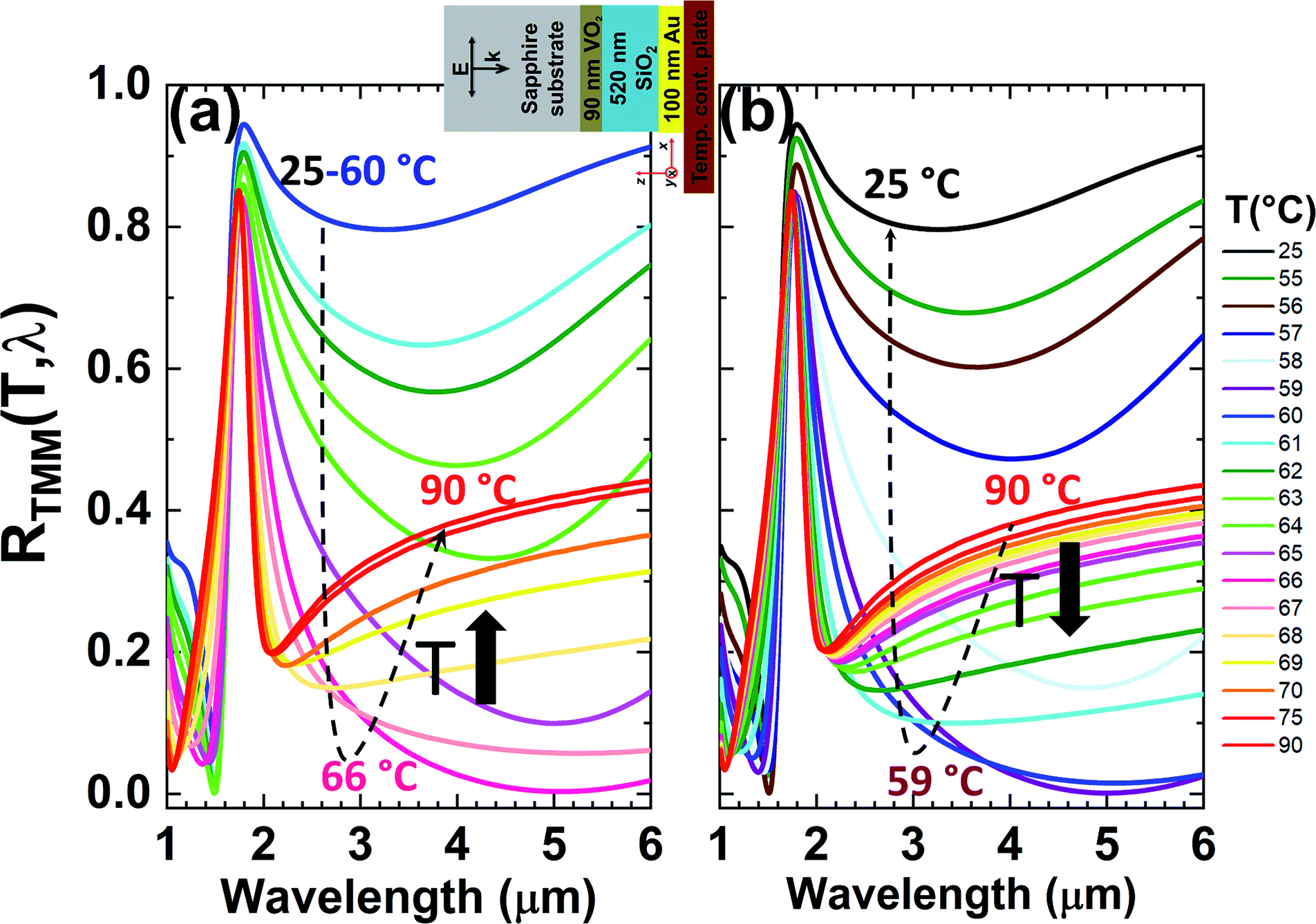 | ||
| Fig. 6 Simulated spectral reflectivity of RTMM(T,λ) of the “sample C” during (a) heating and (b) cooling cycles. Inset (a) is x–z side view of the simulated “sample C” on the temperature stage and illumination conditions. The dashed black curved lines drawn to guide the eye represent the trajectories of the temperatures during heating and cooling. The colored horizontal lines on the right refer to the temperatures applied during heating and cooling. | ||
Conclusions
In conclusion, we conducted an experimental study that included all of the stages, starting from an ultra-thin VO2 film growth, examining the electrical and the optical parameters, extracting the temperature-dependent IR optical parameters, and eventually utilizing these parameters for the demonstration of a dynamic device operating at SWIR and MWIR wavelengths. By analyzing and matching the measured FTIR reflection data with TMM simulations where an EMT is incorporated, we found the spectral optical parameters of the VO2 at the desired temperatures and wavelengths during the heating and cooling stages. Our method explained that not only the volume of metalized VO2 inclusions is directly proportional to the applied temperature, but also for the first time it is unveiled that the shape of metallic inclusions in the VO2 layer differs only in the transition region. Moreover, it was found that all of the hystereses in many different parameters mentioned interestingly have the same value (i.e. ∼7 °C). Finally, we realized the design of a device capable of broadband and tunable reflection that operates at SWIR and MWIR wavelengths by showing all of its stages with experiments and simulations. Additional numerical simulations were carried out to understand the physics behind the operating mechanism, and the angular and the polarization dependency. Our work, which sheds light on all of the stages from material parameters to device application, theoretically and experimentally, contributes to the still vivid field of VO2, which has a lot of optical and photonic applications.Conflicts of interest
The authors declare no conflict of interest.Acknowledgements
E. Ozbay and H. Kurt acknowledge partial support from the Turkish Academy of Sciences (TUBA). This paper includes parts from M. Cihan Cakir's studies that will be presented as his PhD Thesis “Temperature Tunable Nanophotonic Structures”. All of the authors express their gratitude to M. C. Soydan (NANOTAM, Bilkent Unv.) for the ellipsometry measurements of SiO2.References
- A. Cavalleri, T. Dekorsy, H. H. W. Chong, J. C. Kieffer and R. W. Schoenlein, Phys. Rev. B: Condens. Matter Mater. Phys., 2004, 70, 161102 CrossRef.
- F. J. Morin, Phys. Rev. Lett., 1959, 3, 34 CrossRef CAS.
- H. Kocer, S. Butun, E. Palacios, Z. Liu, S. Tongay, D. Fu, K. Wang, J. Wu and K. Aydin, Sci. Rep., 2015, 5, 13384 CrossRef CAS PubMed.
- H. Kocer, S. Butun, B. Banar, K. Wang, S. Tongay, J. Wu and K. Aydin, Appl. Phys. Lett., 2015, 106, 161104 CrossRef.
- H. Kocer, A. Ozer, S. Butun, K. Wang, J. Wu, H. Kurt and K. Aydin, IEEE J. Sel. Top. Quantum Electron., 2019, 25, 1–7 Search PubMed.
- M. J. Dicken, K. Aydin, I. M. Pryce, L. A. Sweatlock, E. M. Boyd, S. Walavalkar, J. Ma and H. A. Atwater, Opt. Express, 2009, 17, 18330–18339 CrossRef CAS PubMed.
- M. R. M. Hashemi, S. H. Yang, T. Wang, N. Sepulveda and M. Jarrahi, Sci. Rep., 2016, 6, 35439 CrossRef CAS PubMed.
- G. Stefanovich, A. Pergament and D. Stefanovich, J. Phys.: Condens. Matter, 2000, 12, 8837–8845 CrossRef CAS.
- Y. Kim, P. C. Wu, R. Sokhoyan, K. Mauser, R. Glaudell, G. K. Shirmanesh and H. A. Atwater, Nano Lett., 2019, 19, 3961–3968 CrossRef CAS PubMed.
- A. Cavalleri, C. Toth, C. W. Siders, J. A. Squier, F. Raksi, P. Forget and J. C. A. Kieffer, Phys. Rev. Lett., 2001, 87, 237401 CrossRef CAS PubMed.
- N. B. Aetukuri, A. X. Gray, M. Drouard, M. Cossale, L. Gao, A. H. Reid, R. Kukreja, H. Ohldag, C. A. Jenkins, E. Arenholz, K. P. Roche, H. A. Dürr, M. G. Samant and S. S. P. Parkin, Nat. Phys., 2013, 9, 661–666 Search PubMed.
- S. Chandra, D. Franklin, J. Cozart, A. Safaei and D. Chanda, ACS Photonics, 2018, 5, 4513–4519 Search PubMed.
- L. Xiao, J. Liu, W. Zhao, Y. Jia, Q. Zhao, K. Liu, Y. Wu, Y. Wei, S. Fan and K. Jiang, Nano Lett., 2015, 15, 8365–8370 CrossRef CAS PubMed.
- M. A. Kats, R. Blanchard, S. Zhang, P. Genevet, C. Ko, S. Ramanathan and F. Capasso, Phys. Rev. X, 2013, 3, 041004 Search PubMed.
- Y. Gao, H. Luo, Z. Zhang, L. Kang, Z. Chen, J. Du, M. Kanehira and C. Cao, Nano Energy, 2012, 1, 221–246 CrossRef CAS.
- T. C. Chang, S. H. Bao, S. D. Ji, H. J. Luo and P. Jin, Adv. Manuf., 2018, 6, 1–19 CrossRef CAS.
- M. Gurvitch, S. Luryi, A. Polyakov and A. Shabalov, J. Appl. Phys., 2009, 106, 104504 CrossRef.
- H. Ma, X. Zhang, Z. Zhang, Y. Wang, G. Wang, F. Liu, R. Cui, C. Huang, M. Wang, Y. Wei, K. Jiang, L. Pan and K. Liu, J. Mater. Chem. C, 2019, 7, 12095–12103 RSC.
- C. Wan, E. H. Horak, J. King, J. Salman, Z. Zhang, Y. Zhou, P. Roney, B. Gundlach, S. Ramanathan, R. H. Goldsmith and M. A. Kats, ACS Photonics, 2018, 5, 2688–2692 CrossRef CAS.
- A. Ozer, H. Kocer and H. Kurt, J. Nanophotonics, 2018, 12, 046022 Search PubMed.
- J. Rensberg, S. Zhang, Y. Zhou, A. S. McLeod, C. Schwarz, M. Goldflam, M. Liu, J. Kerbusch, R. Nawrodt, S. Ramanathan, D. N. Basov, C. Capasso, C. Ronning and M. A. Kats, Nano Lett., 2016, 16, 1050–1055 CrossRef CAS PubMed.
- F. Ligmajer, L. Kejík, U. Tiwari, M. Qiu, J. Nag, M. Konečný, T. Šikola, W. Jin, R. F. F. Haglund, A. Kannatassen and D. Y. Lei, ACS Photonics, 2018, 5, 2561–2567 CrossRef CAS.
- M. Soltani, M. Chaker, E. Haddad, R. V. Kruzelecky and D. Nikanpour, J. Vac. Sci. Technol., A, 2004, 859–864 CrossRef CAS.
- S. Kumar, F. Maury and N. Bahlawane, Sci. Rep., 2016, 6, 37699 CrossRef CAS PubMed.
- F. Ding, S. Zhong and S. I. Bozhevolnyi, Adv. Opt. Mater., 2018, 6, 1701204 CrossRef.
- Z. Song, A. Chen and J. Zhang, Opt. Express, 2020, 28, 2037–2044 CrossRef CAS PubMed.
- R. E. Marvel, R. R. Harl, V. Craciun, B. R. Rogers and R. F. Haglund, Acta Mater., 2015, 91, 217–226 CrossRef CAS.
- K. Liu, S. Lee, S. Yang, O. Delaire and J. Wu, Mater. Today, 2018, 21, 875–896 CrossRef CAS.
- D. P. Partlow, S. R. Gurkovich, K. C. Radford and L. J. Denes, J. Appl. Phys., 1991, 70, 443 CrossRef CAS.
- S. Lu, L. Hou and F. Gan, Adv. Mater., 1997, 9, 244246 CrossRef.
- B. G. Chae, H. T. Kim, S. J. Yun, B. J. Kim, Y. W. Lee, D. H. Youn and K. Y. Kang, Electrochem. Solid-State Lett., 2005, 9, C12 CrossRef.
- C. H. Griffiths and H. K. Eastwood, J. Appl. Phys., 1974, 45, 2201–2206 CrossRef CAS.
- C. C. Y. Kwan, C. H. Griffiths and H. K. Eastwood, Appl. Phys. Lett., 1972, 20, 93–95 CrossRef CAS.
- F. Beteille, L. Mazerolles and L. Livage, Mater. Res. Bull., 1999, 34, 2177–2184 CrossRef CAS.
- D. Brassard, S. Fourmaux, M. Jean-Jacques, J. C. Kieffer and M. A. Khakani, Appl. Phys. Lett., 2005, 87, 051910 CrossRef.
- D. Fu, K. Liu, T. Tao, K. Lo, C. Cheng, B. Liu, R. Zang, H. A. Bechtel and J. Wu, J. Appl. Phys., 2013, 113, 043707 CrossRef.
- D. H. Kim and H. S. Kwok, Appl. Phys. Lett., 1994, 65, 3188–3190 CrossRef CAS.
- Y. X. Guo, Y. F. Liu, C. W. Zou, Z. M. Qi, Y. Y. Wang, Y. Q. Xu, X. L. Wang, F. Zhang and R. Zhou, Appl. Phys. A, 2014, 115, 1245–1250 CrossRef CAS.
- R. McGee, A. Goswami, B. Khorshidie, K. McGuire, K. Schofield and T. Thundant, Acta Mater., 2017, 137, 12–21 CrossRef CAS.
- R. L. Remke, R. M. Walser and R. W. Bene, Thin Solid Films, 1979, 61, 73–82 CrossRef CAS.
- C. B. Greenberg, Thin Solid Films, 1983, 110, 73–82 CrossRef CAS.
- Y. Takahashi, M. Kanamori, H. Hashimoto and Y. Moritani, J. Mater. Sci., 1989, 24, 192–198 CrossRef CAS.
- T. Maruyama and Y. Ikuta, J. Mater. Sci., 1993, 28, 5073–5078 CrossRef CAS.
- T. D. Manning, I. P. Parkin, M. E. Pemble, D. Shell and D. Vernardou, Chem. Mater., 2004, 16, 744–749 CrossRef CAS.
- J. Nag and R. F. Haglund, J. Phys.: Condens. Matter, 2008, 20, 264016 CrossRef.
- D. H. Kim and H. S. Kwok, Appl. Phys. Lett., 1994, 65, 3188–3190 CrossRef CAS.
- Y. Muraoka and Z. Hiroi, Appl. Phys. Lett., 2002, 80, 583–585 CrossRef CAS.
- K. Okimura and N. Kubo, Jpn. J. Appl. Phys., 2005, 44, 1150–1153 CrossRef.
- Z. Yang, C. Ko and S. Ramanathan, J. Appl. Phys., 2010, 108, 073708 CrossRef.
- Y. Zhou and S. Ramanathan, J. Appl. Phys., 2012, 112, 074114 CrossRef.
- H. Kim, Y. Kim, K. S. Kim, H. Y. Jeong, A.-R. Jang, S. H. Han, D. H. Yoon, K. S. Sulh, H. S. Shin, T. Y. Kim and W. S. Yang, ACS Nano, 2013, 7, 5769–5776 CrossRef CAS PubMed.
- S. Genchi, M. Yamamoto, K. Shigematsu, S. Aritomi, R. Nouchi, T. Kanki, K. Watanabe, T. Tabiguchi, Y. Murakami and H. Tanaka, Sci. Rep., 2019, 9, 2857 CrossRef PubMed.
- C. Wan, Z. Zhang, D. Woolf, C. M. Hessel, J. Rensberg, J. M. Hensley, Y. Xiao, A. Shahsafi, J. Salman, S. Richter, Y. Sun, M. M. Qazilbash, R. Schmidt-Grund, C. Ronning, S. Ramanathan and M. A. Kats, Ann. Phys., 2019, 531, 1900188 CrossRef CAS.
- P. Yeh, Optical Waves in Layered Media, Wiley, 2005 Search PubMed.
- H. Kocer, S. Butun, Z. Li and K. Aydin, Sci. Rep., 2015, 5, 8157 CrossRef PubMed.
- Lumerical page, https://www.lumerical.com/products/fdtd/ Search PubMed.
- M. A. Kats, D. Sharma, J. Lin, P. Genevet, R. Blanchard, Z. Yang, M. M. Qazilbash, D. N. Basov, S. Ramanathan and F. Capasso, Appl. Phys. Lett., 2012, 101, 221101 CrossRef.
- H. Looyenga, Dielectric constants of mixtures, Physica, 1965, 31, 401–406 CrossRef CAS.
- E. D. Palik, Handbook of Optical Constants of Solids, Elsevier, 1998 Search PubMed.
- H. Hajian, A. Ghobadi, B. Butun and E. Ozbay, J. Opt. Soc. Am. B, 2019, 36, F131–F143 CrossRef CAS.
- A. Ghobadi, H. Hajian, B. Butun and E. Ozbay, ACS Photonics, 2018, 5, 4203–4221 CrossRef CAS.
Footnote |
| † Electronic supplementary information (ESI) available: The measured and simulated spectral reflectivity maps of “sample A” during heating and cooling, maps of extracted infrared spectral optical parameters of VO2 in “sample A” during heating and cooling, additional hysteretic behaviors, ellipsometer spectral data for SiO2, numerical simulations to enlighten the physics behind the operating mechanism of the tunable device (SuppInfo1). Moving one and two-dimensional spatial representation of electric fields at T = 25 °C and T = 90 °C calculated for “sample C” at a wavelength of 4 μm (SuppInfo2). See DOI: 10.1039/d0ra05890d |
| This journal is © The Royal Society of Chemistry 2020 |