
 Open Access Article
 This Open Access Article is licensed under a Creative Commons Attribution-Non Commercial 3.0 Unported Licence
Growth process control produces high-crystallinity and complete-reaction perovskite solar cells†
Chun-Hsiao Kuana,
Po-Tsun Kuob,
Cheng-Hung Hou d,
Jing-Jong Shyuede and
Ching-Fuh Lin*abc
d,
Jing-Jong Shyuede and
Ching-Fuh Lin*abc
aGraduate Institute of Photonics and Optoelectronics, National Taiwan University, No. 1, Sec. 4, Roosevelt Road, Taipei, 10617, Taiwan. E-mail: lincf@ntu.edu.tw
bGraduate Institute of Electronics Engineering, National Taiwan University, No. 1, Sec. 4, Roosevelt Road, Taipei, 10617, Taiwan
cDepartment of Electrical Engineering, National Taiwan University, No. 1, Sec. 4, Roosevelt Road, Taipei, 10617, Taiwan
dResearch Center for Applied Sciences, Academia Sinica, Taipei 11529, Taiwan
eDepartment of Materials Science and Engineering, National Taiwan University, Taipei 10617, Taiwan
First published on 30th September 2020
Abstract
The growth process control (GPC) method, a new method which is better than thermal evaporation, for producing high-crystallinity perovskites by controlling the growth time in a low vacuum, is explored in this work. Inspired by evaporation technology, GPC is an effective method for modifying traditional thermal evaporation and for controlling the crystal growth of perovskite CH3NH3I3. Compared to fabrication with the process of co-evaporation, the MAPbI3 perovskite solar cell fabricated by GPC has high uniformity and film coverage. All of the manufacturing is carried out outside of the glove box. It provides an easy and effective way for perovskite fabrication for industrialization. Here, after using GPC to form perovskite solar cells, the residual methylammonium iodide (MAI) and PbI2 which is produced by the evaporation process can react completely, observed by time of flight secondary ion mass spectrometry (TOF-SIMS). Finally, formed by GPC, perovskite solar cells exhibit high performance and fewer crystal defects. The electron and hole recombination is greatly reduced. Through the GPC method, the Jsc and the filling factor are improved with the increase of time after the fabrication. The power conversion efficiency was increased from 11.12% to 16.4%.
Introduction
In 2009, the organic–inorganic mixed lead halide perovskite solar cell (MAPbI3), first proposed by Miyasaka, became a high-potential material due to its low cost and rapid efficiency.1–3 The excellent photoelectric properties28 of perovskites are beneficial to apply in various fields such as photovoltaics4,5,31 and photoelectric detection.6–8 The traditional perovskite as a light-harvesting active layer is mainly based on MAPbI3, which is primarily composed of MAI and lead iodide 1![[thin space (1/6-em)]](https://www.rsc.org/images/entities/char_2009.gif) :1. MAPbI3 has the typical structure of a perovskite such as ABX3.32 There are various phases in MAPbI3, depending on the growth temperature. When the temperature is higher than 330 K, MAPbI3 is in the cubic phase. The cubic phase of the crystal structure of MAPbI3 with a high temperature has the largest amount of electronic conductivity. Perovskite, as a new absorption layer in solar cells, has a good absorption coefficient, high electron–hole diffusion length, and carrier mobility under a suitable energy gap. The fabrication of MAPbI3 as an active layer is mainly divided into a one-step solution process,33 two-step solution process9,10,29,30,34 and thermal evaporation.11,12 The one-step solution process is mainly about spin coating MAPbI3, which is formed with MAI and PbI2 powder dissolved in dimethylformamide (DMF) and dimethyl sulfoxide (DMSO), on the indium tin oxide (ITO) substrate, which has been spin-coated with poly(3,4-ethylenedioxythiophene) polystyrene sulfonate (PEDOT:PSS). The two-step solution process involves preparing MAI and PbI2 dissolved in different solvents and spinning them, respectively, on the hole transport layer to synthesize MAPbI3. Although the cost of the solution process27 is low and the operation is not complex, the error tolerance is low in the industrial production of devices. Thermal evaporation is composed of two or more solid materials (such as MAI and PbI2 powder) that react with each other on the substrate evaporated by constant temperature or by electron beam heating in a high vacuum.24,25 In recent years, doping engineering and solvent engineering have also been developed to improve the crystallization of perovskite.26 Because the procedure of solid evaporation is stable, the fabrication of perovskite as an active layer via thermal evaporation has a high yield, but the price of this is relatively high. In addition, the perovskite solar cell made via thermal evaporation is easy to decompose at a high temperature, and it may cause the problem of the incomplete reaction of MAI and PbI2, seriously affecting the transmission of electrons and holes. Although using thermal evaporation can stably produce a large number of perovskite solar cells, problems such as excess PbI2 and the easy decomposition of MAI restrict the development of mass production. Therefore, the vapor-assisted solution process (VSVP)13 developed in recent years combines the advantages of the solution process and the thermal evaporation, which can not only reduce the cost of evaporation but also improve the error tolerance in production.
:1. MAPbI3 has the typical structure of a perovskite such as ABX3.32 There are various phases in MAPbI3, depending on the growth temperature. When the temperature is higher than 330 K, MAPbI3 is in the cubic phase. The cubic phase of the crystal structure of MAPbI3 with a high temperature has the largest amount of electronic conductivity. Perovskite, as a new absorption layer in solar cells, has a good absorption coefficient, high electron–hole diffusion length, and carrier mobility under a suitable energy gap. The fabrication of MAPbI3 as an active layer is mainly divided into a one-step solution process,33 two-step solution process9,10,29,30,34 and thermal evaporation.11,12 The one-step solution process is mainly about spin coating MAPbI3, which is formed with MAI and PbI2 powder dissolved in dimethylformamide (DMF) and dimethyl sulfoxide (DMSO), on the indium tin oxide (ITO) substrate, which has been spin-coated with poly(3,4-ethylenedioxythiophene) polystyrene sulfonate (PEDOT:PSS). The two-step solution process involves preparing MAI and PbI2 dissolved in different solvents and spinning them, respectively, on the hole transport layer to synthesize MAPbI3. Although the cost of the solution process27 is low and the operation is not complex, the error tolerance is low in the industrial production of devices. Thermal evaporation is composed of two or more solid materials (such as MAI and PbI2 powder) that react with each other on the substrate evaporated by constant temperature or by electron beam heating in a high vacuum.24,25 In recent years, doping engineering and solvent engineering have also been developed to improve the crystallization of perovskite.26 Because the procedure of solid evaporation is stable, the fabrication of perovskite as an active layer via thermal evaporation has a high yield, but the price of this is relatively high. In addition, the perovskite solar cell made via thermal evaporation is easy to decompose at a high temperature, and it may cause the problem of the incomplete reaction of MAI and PbI2, seriously affecting the transmission of electrons and holes. Although using thermal evaporation can stably produce a large number of perovskite solar cells, problems such as excess PbI2 and the easy decomposition of MAI restrict the development of mass production. Therefore, the vapor-assisted solution process (VSVP)13 developed in recent years combines the advantages of the solution process and the thermal evaporation, which can not only reduce the cost of evaporation but also improve the error tolerance in production.
In our study, the original VSVP was modified via a method that our lab invented, the so-called sandwich evaporation technique (SET).14,15 In addition, the growth process control (GPC) method further improved the SET. MAPbI3 is formed via the reaction of MAI–PbI2–MAI. The formation rate of MAPbI3 can be controlled by using MAI as a bottom layer, as well as double diffusion (MAI forms the upper and lower layers diffused to PbI2; this results in better planeness). In addition, through using MAI as the bottom layer, the grains with a uniform orientation can be obtained, which is beneficial for carrier separation and photocurrent generation. On the basis of double diffusion, we found that MAPbI3 formed via the evaporation of MAI–PbI2–MAI would crystallize gradually with time, and the performance of the solar cell would improve after several days of storage and controlling in a low vacuum. We call it GPC technology. The concepts of double diffusion and a seed layer promoted the crystallization of perovskite films. The perovskite solar cells fabricated by GPC finally reached a power conversion efficiency (PCE) of 16.4%.
Fabrication
The fabrication of perovskite solar cells is schematically shown in Fig. 1. ITO substrates were cleaned using acetone, isopropyl alcohol, and methanol for 15 min, then treated with UV-ozone for 10 min. Next, the treated ITO-coated substrates were spin-coated with PEDOT:PSS (PEDOT-4083, purchased from CLEVIOTM) at 3000 rpm for 30 s and annealed at 120 °C for 15 min in the air. The solution of CH3NH3I (MAI) dissolved in dimethylformamide (DMF) with 20 mg ml−1, and was spin-coated onto the transport layer as the bottom layer at 3000 rpm for 30 s and annealed at 100 °C for 10 min in the air. After drying, the PbI2 was evaporated on the precursor layers with a thickness of 185 nm via evaporator with the rate of 0.03 nm s−1. Then, the MAI powder was evaporated by the homemade SET chamber to form perovskite for 30 min. The size of the homemade SET chamber is 2800 cm3 and the distance between sample and MAI powder is 7.5 cm. The remaining MAI was cleaned by spin-coating isopropanol (IPA) at 3000 rpm for 30 s and annealed at 100 °C for 5 minutes to get a smooth surface and a deep-brown-color perovskite layer. Then it was annealed at 120 °C with spin-coating PC60BM (phenyl-C60-butyric acid methyl ester) onto the perovskite/PEDOT:PSS/ITO substrate at 1300 rpm for 60 s. Finally, the BCP and the silver were evaporated by thermal deposition with thicknesses of 5 nm and 120 nm, respectively. All of our devices were preserved in a low-vacuum chamber at 0.13 Pa on the first day to the seventh day for controlling the growth process (MAI and PbI2), and they were measured in the ambient atmosphere at room temperature. | ||
| Fig. 1 Fabrication of perovskite solar cells. | ||
Result and discussion
In the solution process,16–23 MAPbI3 needed to be manufactured in a nitrogen environment. However, in this research, all of the coating and annealing processes were carried out outside of the glove box. This would contribute to mass production and to the reduction of cost. For device fabrication, the solution process depends on the friction generated from the solution coated on the substrate. This could cause poor film coverage and uniformity, in addition to problems of bad crystallization or too small particle size due to the formation of a perovskite active layer in a short period of time. However, the SET can be used to improve the quality of the film.After all of the components were completed, we measured the perovskite solar cells for the first time. Our device was kept in a low-vacuum state for several days, and then, the efficiency of the device was measured and observed repeatedly. We found that the performance of our perovskite solar cells gradually improved with the increase of time. In addition, the open circuit voltage, short circuit current, and filling factor were significantly improved. Therefore, we call this GPC post-treatment technology, which combines the SET and low-vacuum controlling. Besides, after making perovskite solar cells by sandwich evaporation method, we keep our devices at room temperature. The low temperature helps the GPC process proceed at a slow rate. Using GPC post-treatment technology, we found that the crystallization of MAPbI3 perovskite became better. Solar cells with MAPbI3 as the active layer had relatively higher photoelectric conversion efficiency. This is not only of great significance to the large-scale production of perovskite solar cells but also it has the opportunity to improve the efficiency of various components of perovskite materials. Our perovskite solar cells adopted the pin structure of ITO/PEDOT:PSS/MAPbI3/PC60BM/BCP/Ag.
In the traditional evaporation process, MAI and PbI2 are respectively or simultaneously heated and evaporated in a high-vacuum evaporation machine to form MAPbI3. This is called thermal evaporation or the co-evaporation method, respectively. Being heated by the evaporator to evaporate MAI and PbI2 can make the reaction rate more uniform, and MAPbI3 with a better surface quality can be made. However, the evaporation time and required temperature of PbI2 and MAI are different. MAI as an organic material is easy to decompose at a high temperature.


Therefore, it is hard to control the evaporative rate of MAI, and this will cause an excess of PbI2. The residual PbI2 will block the separation of electron holes and affect the transmission of a photocurrent. Therefore, in this study, MAI as a bottom layer dissolved in DMF was spin-coated on the substrate that grew PEDOT:PSS. PbI2 and MAI were evaporated by SET, respectively, through the thermal evaporator and SET, just like a sandwich: PbI2 was in the middle and was used to have double diffusion for the reaction of MAI and PbI2.
In order to demonstrate that GPC could effectively overcome the difficulties of incomplete reaction between MAI and PbI2 in traditional evaporation method, time of flight secondary ion mass spectrometry (TOF-SIMS) was used to measure the depth distribution of elements in MAPbI3, which was formed by SET and GPC post-processing technology. The C60 acted as excitation source in TOF-SIMS, which was able to not only avoid the damage of organic cation as CH3NH3I+(MA+) caused by high energy source generated by Ar+ as excitation source in SIMS, but also acquire the information of the depth distribution of MA+ metal ion of lead (Pb2+) and the ion of iodine (I−) in perovskite, simultaneously. As shown in Fig. 2, we utilized the SIMS to check the element distribution in different stages of SET with and without GPC post treatment.
 | ||
| Fig. 2 (a) MAI as seed layer was spin-coated on ITO which was coated with PEDOT:PSS. (b and c) PbI2 and MAI power was evaporated on the MAI seed layer by homemade SET chamber, respectly. (d) The depth distribution with PbI2 being evaporated on the MAI seed layer, (e) MAI powder was evaporated as the top layer without GPC, (f) MAI powder was evaporated as the top layer with GPC for 4 days and (g) for a week later. (h) The principle for the GPC. | ||
Fig. 2(d) shows the distribution of elements. Part of the organic macromolecular group MA+ penetrated into PbI2, and the rest of MA+ was retained at the border of PbI2 and ITO. Fig. 2(c) shows the double diffusion by adopting SET to complete the upper-layer of MAI. The double diffusion enables the MAI to gradually combine with PbI2 to form MAPbI3. From the depth element distribution measured in Fig. 2(e), we found that there was a great quantity of PbI2 in the newly completed components. It would be an energy barrier between the active layer and the hole transform layer, which hinders the transfer of carriers. This was also the reason why traditional evaporation method cannot be carried out in the large-scale production. Although the perovskite solar cells produced in the evaporation process have better flatness and fewer defects than the production in the solution process, residue of PbI2 seriously hinders the separation and transmission of carriers, which was fatal for solar energy. Therefore, we introduce GPC post-processing treatment to preserve our devices after a few days under low vacuum condition. We found that the excessive PbI2 gradually decreased. Fig. 2(f) shows that the content of PbI2 significantly reduces after four days of GPC treatment. Fig. 2(g) shows that the PbI2 entirely disappears after one week of GPC treatment, and the MAI and PbI2 react completely, which is very exciting for the large-scale production of perovskite solar cells by vaporization. The whole reaction of GPC post treatment is shown in Fig. 2(h). The distribution of elements in CH3NH3PbI3 is discussed in ESI.†
Compared with the traditional evaporation method, GPC can effectively deal with residual PbI2. In general, if the PbI2 film is too thin, the MAI cannot penetrate it effectively and form perovskite crystals completely. In addition, the influence of insufficient permeability can be reduced by using double diffusion. However, the discontinuous infiltration of MAI may cause a decrease in the number of crystalline particles. Due to the double diffusion of MAI–PbI2–MAI, the perovskite solar cells can be stored in a low vacuum after fabrication, which is beneficial for the diffusion of MAI from the upper and lower layers to the sandwich's intermediate layer, and then, the growth of the perovskite in the active layer can be controlled until it completely reacts.
The high-crystallinity MAPbI3 perovskite active layer can be made, and then, the perovskite solar cells with excellent performance can be produced. By using GPC, we analyzed the film change of the perovskite as an active layer, as shown in Fig. 3.
 | ||
| Fig. 3 The perovskite solar cells made via GPC with (a) XRD of 2theta for 5–50 degrees, (b) 2theta for 15–50 degrees, (c) absorption, and (d) PL on different days. | ||
Fig. 3 (a) and (b) show the X-ray Diffraction (XRD) patterns of X-ray with angles of 0 to 50 degrees and 15 to 50 degrees treated with GPC for 1 day, 3 days, 5 days, and 7 days. According to the 2theta angles measured by XRD, it can be found that at 2theta = 12.6°, it is mainly the crystallization of PbI2 in the direction of (0,0,1), whereas the main crystallization peaks of perovskite appear at 2theta = 14.05° (1,1,0), 28.41° (2,2,0), 31.7° (3,1,0). The crystallization of MAPbI3 as an active layer and the bond of Pb–I in PbI2 can be shown by X-ray diffraction. We can see that the strength of the main peak of the perovskite made on the first day is about 2500, and the strength of the main peak gradually rises with the GPC for several days. This proves that the crystal state of the perovskite, which is controlled for several days in a low vacuum, became better. We can see that the intensity increased with time, and the maximum diffraction intensity is more than 5000. Fig. 3(c) shows the absorption of perovskite for the first to seventh day, which was made via GPC. The absorption spectrum can be used to characterize the storage capacity of photons in different wavelengths. If the absorption of the photons of the perovskite active layer is stronger, the probability of conversion to electrons will be higher. Therefore, the absorption of perovskite improved with time, and the probability of photons converting into a photocurrent increased. This was beneficial for the improvement of the short-circuit current. Fig. 3(d) shows the photoluminescence (PL) spectrum of the perovskite fabricated via GPC for 1 to 6 days. The band gap of the photoluminescence spectrum of perovskite is similar to that of the absorption spectrum. Therefore, the stronger the photoluminescence, the fewer the impurities between energy bands due to defects, and the less leakage current one has, which is beneficial for the improvement of the short-circuit current. The luminous wavelength of MAPbI3 is about 750 nm, and we can see that the spectral intensity increased for the same phenomenon. After GPC, the reaction of MAPbI3 is gradually completed, so the absorption of perovskite is improved. Hence more photons are converted into electrons. After the GPC process, the TOF-SIMS shows that PbI2 is completely eliminated, and then the energy level barrier caused by PbI2 disappears. It is conducive to the improvement of short-circuit current after solving the problem of residual PbI2 which often occurs in the traditional evaporation technology.
In this research, we measured the J–V curves of day 1, and a week later, respectively, as shown in Fig. 4(a). The voltage and current density of Fig. 4(a) at different times show that the perovskite made via the SET will be preserved in a low vacuum for several days, the performance will be significantly improved, and each index will be further optimized. The comparison of perovskite solar cells is given in ESI.† Fig. 4(b) shows the number of devices which are treated with and without GPC. Our devices show good reproducibility, the efficiency is located from 11.2% to 16.4% for nearly 40 devices, and most of the PCEs are about 13%. Therefore, the champion device reached the maximum efficiency as 16.4% on a week later. The curve represents the Gaussian function of the histogram. The specific numerical parameters are shown in Table 1 below. Therefore, the perovskite solar cells fabricated via GPC can reach a comparably high efficiency as long as the growing time is effectively controlled. This is beneficial for industrial production.
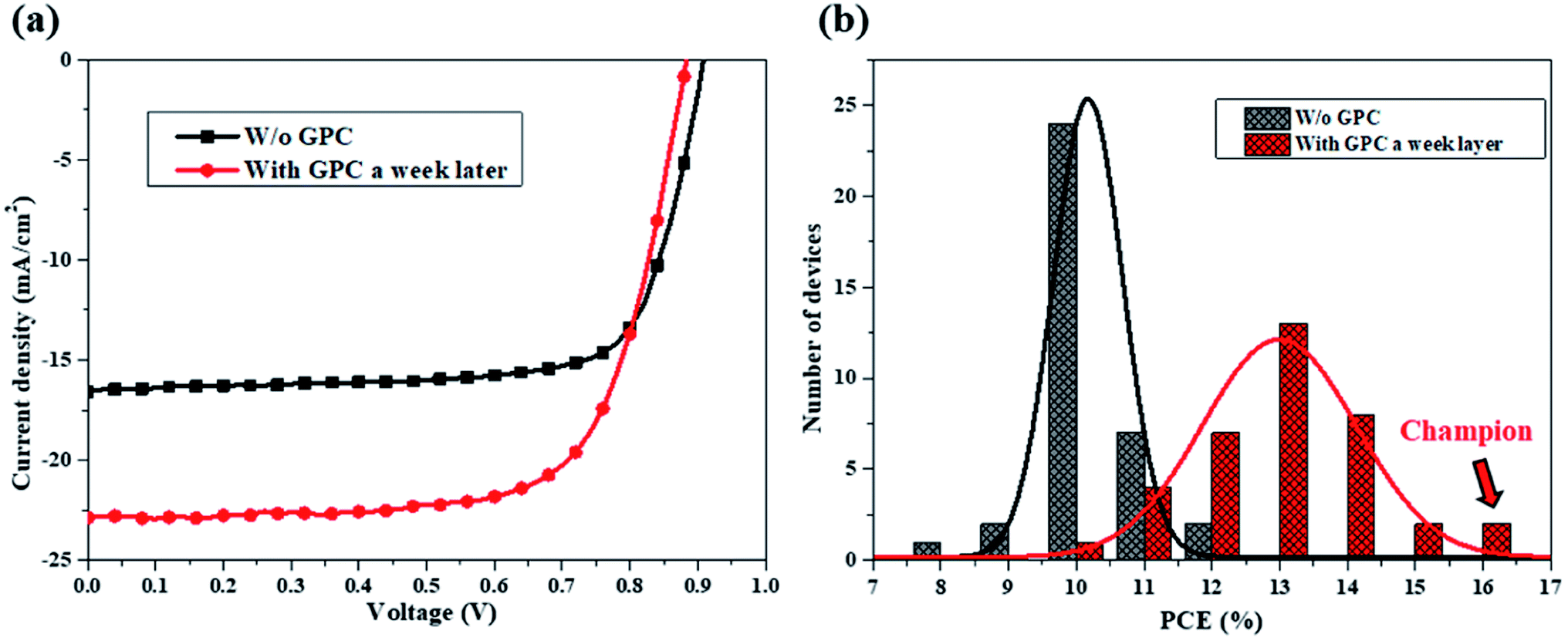 | ||
| Fig. 4 (a)Number of device (b) J–V curve, of perovskite solar cells prepared w/o GPC and with GPC a week later. | ||
| GPC | Voc (V) | Jsc (mA cm−2) | FF (%) | PCE (%) |
|---|---|---|---|---|
| W/o GPC | 0.91 | 16.60 | 73.80 | 11.12 |
| With GPC for a week later | 0.91 | 23.79 | 76.20 | 16.43 |
Furthermore, solar cells often need process of aging, and the completion time of components is determined by the time when the cells are made. Therefore, compared with the traditional evaporation method, our SET to form perovskite solar cell can reduce the time of fabrication, the GPC process can slow down the crystallization rate of the film and enable the large crystals to gradually form. Thus, it is conducive to industrial production. The component statistics of perovskite solar cells with and without GPC are given in ESI.†
As shown in Fig. 5(c), the SEM showed the cross-section of the new perovskite formed by GPC. It could be seen from the figure that the perovskite solar cell was completed without GPC. There existing a layer of an incomplete reaction PbI2 hinders the carrier transport. In comparison, the PbI2 residual layer disappeared, and the cross-section of perovskite became more uniform, as shown in Fig. 5(d) for the SEM image of the perovskite preserved in a low vacuum for a week. We speculate that the reaction speed of PbI2 and MAI will slow down in the condition of a low vacuum. Keeping the perovskite solar cell in the vacuum state is beneficial for controlling the formation rate of MAPbI3, and a perovskite material with better crystallinity can be obtained. From the cross-sections taken with SEM without GPC and with GPC for a week later, we found that the particles in the newly completed perovskite active layer were smaller. There were many gaps between crystals of perovskite, and they are not uniform in the beginning. However, after a week of low-vacuum control, the speed of crystallization in the low-vacuum state becomes slower, the crystallinity gradually becomes better, and the defects are decreased. This is very helpful for reducing the leakage current and for the improvement of the short-circuit current.
 | ||
| Fig. 5 SEM cross-section (a) without GPC and (b) with GPC for a week later at 20000 times magnification. (c) Without GPC and (d) with GPC for a week later at 50000 times magnification. | ||
Fig. 6 below shows a summary of the statistical results of parameters with and w/o GPC post-processing of perovskite solar cell devices made with SET. After the GPC, the figure shows that (a) Voc, (b) Jsc and (c) fill factor are improved, and the quality of the perovskite film is tuned into better condition. (d) Rs decreases due to the reduction of excess reactant hindrance like PbI2.
 | ||
| Fig. 6 The number of devices for (a) Voc, (b) Jsc, (c) FF, (d) Rs of MAPbI3 perovskite solar cell which was made without GPC and with GPC for a week later. | ||
Conclusion
It is difficult to produce perovskite solar cells on a large scale through the solution process only, whereas the perovskite fabricated via the thermal evaporation process has a good yield and high error tolerance. However, there are some problems. For example, it is hard for the synthetic materials of perovskite (such as MAI and PbI2) to react completely, which will cause an unnecessary energy band to affect the transmission of electronic and hole. In addition, it will make the cost of fabrication relatively high. In this study, the MAI dissolved in DMF was used as the bottom layer to evaporate PbI2 and MAI with SET, and the final device was kept in a low vacuum for a period of time. Preservation in a low vacuum slows down the formation of MAPbI3. This made the crystallinity of CH3NH3I3 as an active layer better, and the device performance was further improved. The optimized perovskite solar cell experienced excellent improvement with Jsc = 23.79 mA cm−2, Voc = 0.91 V, FF = 76.2%, and PCE = 16.43%, respectively. In addition, the entire process was carried out outside of the glove box, which was beneficial for the experimental operation and cost savings. Furthermore, this method is beneficial for industrial production.Methods
Current density–voltage (J–V) characteristics were measured with a Keithley 2400 source under AM 1.5G at an intensity of 1000 W m−2. X-ray diffraction (XRD) data were collected using an X-ray powder diffractometer PW3040 with Cu-Kα radiation. Scanning electron microscopy (SEM) images were analyzed on a JEOL JSM-7600F microscope using a 10 kV field emission.All time-of-flight secondary-ion mass spectrometry (ToF-SIMS) depth profiles were acquired using a PHI TRIFT V nanoTOF (ULVAC-PHI, Japan) system with a dual beam sputter-and-view scheme. In the analysis phase, a pulsed C60+ (approximately 8200 Hz, pulse length of 15 ns) rastering over a 100 μm × 100 μm area was applied as the primary ion. The acceleration voltage of the incident C60+ ion was 20 kV and the beam current was 0.08 nA-DC. As for the sputter phase, a 3 kV Ar+ beam with beam current of 100 nA rastering over a 1500 μm × 1500 μm area was utilized to remove the top surface material. These parameters were determined based on our previous study to eliminate the depth profile artifacts of perovskite materials.35
All the XPS spectra were acquired by a PHI 5000 VersaProbe (ULVAC-PHI, Japan) system. During data acquisition, a monochromatic Al Kα X-ray beam with diameter of 100 μm was illuminated on the sample surface while it was neutralized by an e− and an Ar+ beam, both with an acceleration voltage of 10 V, to avoid surface potential build-up.
Conflicts of interest
There are no conflicts to declare.Acknowledgements
We gratefully acknowledge Ministry of Science and Technology in Taiwan for supporting the research with the contract numbers: MOST 107-2221-E-002-172-MY3, MOST 107-2221-E-002-155-MY3, MOST 108-2221-E-002-145-MY3.References
- M. A. Green, A. Ho-Baillie and H. J. Snaith, Nat. Photonics, 2014, 8, 506–514 CrossRef CAS.
- H. J. Snaith, J. Phys. Chem. Lett., 2013, 4, 3623–3630 CrossRef CAS.
- S. Shahbazi, F. Tajabadi, H. S. Shiu, R. Sedighi, E. Jokar, S. Gholipour, N. Taghavinia, S. Afshar and E. W. G. Diau, RSC Adv., 2016, 6, 65594–65599 RSC.
- Q. Jiang and T. Xu, Comments Inorg. Chem., 2016, 36, 200–214 CrossRef CAS.
- X. Chen, Z. Jia, Z. Chen, T. Jiang, L. Bai, F. Tao, J. Chen, X. Chen, T. Liu and X. Xu, Joule, 2020, 4(7), 1594–1606 CrossRef CAS.
- R. Zhuang, X. Wang, W. Ma, Y. Wu, X. Chen, L. Tang, H. Zhu, J. Liu, L. Wu and W. Zhou, Nat. Photonics, 2019, 13, 602–608 CrossRef CAS.
- Y. Su, W. Ma and Y. M. Yang, J. Semicond., 2020, 41, 051204 CrossRef CAS.
- W. Zhu, W. Ma, Y. Su, Z. Chen, X. Chen, Y. Ma, L. Bai, W. Xiao, T. Liu and H. Zhu, Light: Sci. Appl., 2020, 9, 1–10 CrossRef.
- P. W. Liang, C. Y. Liao, C. C. Chueh, F. Zuo, S. T. Williams, X. K. Xin, J. J. Lin and A. K. Y. Jen, Adv. Mater., 2014, 26, 3748–3754 CrossRef CAS.
- D. Y. Liu and T. L. Kelly, Nat. Photonics, 2014, 8, 133–138 CrossRef CAS.
- M. Liu, M. B. Johnston and H. J. Snaith, Nature, 2013, 501, 395–398 CrossRef CAS.
- M. D. Xiao, F. Z. Huang, W. C. Huang, Y. Dkhissi, Y. Zhu, J. Etheridge, A. Gray-Weale, U. Bach, Y. B. Cheng and L. Spiccia, Angew. Chem., Int. Ed., 2014, 53, 9898–9903 CrossRef CAS.
- Q. Chen, H. P. Zhou, Z. R. Hong, S. Luo, H. S. Duan, H. H. Wang, Y. S. Liu, G. Li and Y. Yang, J. Am. Chem. Soc., 2014, 136, 622–625 CrossRef CAS.
- P. T. Kuo, S. P. Lin, H. C. Hsu and C. F. Lin, IEEE Journal of Photovoltaics, 2018, 8, 777–782 Search PubMed.
- S.-P. Lin, S.-K. Chang, H.-C. Lee, P.-T. Guo, S. Thiyagu and C.-F. Lin, IEEE Journal of Photovoltaics, 2016, 7, 184–190 Search PubMed.
- P. Docampo, F. C. Hanusch, S. D. Stranks, M. Döblinger, J. M. Feckl, M. Ehrensperger, N. K. Minar, M. B. Johnston, H. J. Snaith and T. Bein, Adv. Energy Mater., 2014, 4, 1400355 CrossRef.
- Y. Zhao and K. Zhu, J. Phys. Chem. C, 2014, 118, 9412–9418 CrossRef CAS.
- Q. Wang, Y. Shao, Q. Dong, Z. Xiao, Y. Yuan and J. Huang, Energy Environ. Sci., 2014, 7, 2359–2365 RSC.
- C.-H. Chiang, Z.-L. Tseng and C.-G. Wu, J. Mater. Chem. A, 2014, 2, 15897–15903 RSC.
- M. J. Carnie, C. Charbonneau, M. L. Davies, J. Troughton, T. M. Watson, K. Wojciechowski, H. Snaith and D. A. Worsley, Chem. Commun., 2013, 49, 7893–7895 RSC.
- J. You, Z. Hong, Y. Yang, Q. Chen, M. Cai, T.-B. Song, C.-C. Chen, S. Lu, Y. Liu and H. Zhou, ACS Nano, 2014, 8, 1674–1680 CrossRef CAS.
- W. Nie, H. Tsai, R. Asadpour, J.-C. Blancon, A. J. Neukirch, G. Gupta, J. J. Crochet, M. Chhowalla, S. Tretiak and M. A. Alam, Science, 2015, 347, 522–525 CrossRef CAS.
- J.-H. Im, H.-S. Kim and N.-G. Park, APL Mater., 2014, 2, 081510 CrossRef.
- J. Burschka, N. Pellet, S.-J. Moon, R. Humphry-Baker, P. Gao, M. K. Nazeeruddin and M. Grätzel, Nature, 2013, 499, 316–319 CrossRef CAS.
- M. Becker and M. Wark, Org. Electron., 2017, 50, 87–93 CrossRef CAS.
- J. Chen, J. Xu, C. X. Zhao, B. Zhang, X. L. Liu, S. Y. Dai and J. X. Yao, ACS Appl. Mater. Interfaces, 2019, 11, 4597–4606 CrossRef CAS.
- G. E. Eperon, V. M. Burlakov, P. Docampo, A. Goriely and H. J. Snaith, Adv. Funct. Mater., 2014, 24, 151–157 CrossRef CAS.
- A. Fahrenbruch and R. Bube, Fundamentals of solar cells: photovoltaic solar energy conversion, Elsevier, 2012 Search PubMed.
- J.-H. Im, I.-H. Jang, N. Pellet, M. Grätzel and N.-G. Park, Nat. Nanotechnol., 2014, 9, 927 CrossRef CAS.
- K. Liang, D. B. Mitzi and M. T. Prikas, Chemistry of Materials, 1998, 10, 403–411 CrossRef CAS.
- Y. Ren, Y. Cao, D. Zhang, S. M. Zakeeruddin, A. Hagfeldt, P. Wang and M. Grätzel, Adv. Mater., 2020, 2000193 CrossRef CAS.
- T.-B. Song, Q. Chen, H. Zhou, C. Jiang, H.-H. Wang, Y. M. Yang, Y. Liu, J. You and Y. Yang, J. Mater. Chem. A, 2015, 3, 9032–9050 RSC.
- Y. Y. Wang, N. N. Song, L. Feng and X. Y. Deng, ACS Appl. Mater. Interfaces, 2016, 8, 24703–24711 CrossRef CAS.
- S. Yang, Y. Chen, Y. C. Zheng, X. Chen, Y. Hou and H. G. Yang, RSC Adv., 2015, 5, 69502–69508 RSC.
- C.-H. Hou, S.-H. Hung, L.-J. Jhang, K.-J. Chou, Y.-K. Hu, P.-T. Chou, W.-F. Su, F.-Y. Tsai, J. Shieh and J.-J. Shyue, ACS Appl. Mater. Interfaces, 2020 Search PubMed.
Footnote |
| † Electronic supplementary information (ESI) available. See DOI: 10.1039/d0ra05772j |
| This journal is © The Royal Society of Chemistry 2020 |