
 Open Access Article
 This Open Access Article is licensed under a Creative Commons Attribution-Non Commercial 3.0 Unported Licence
Stability of MAPbI3 perovskite grown on planar and mesoporous electron-selective contact by inverse temperature crystallization†
Ramya Krishna Battula abc,
Ganapathy Veerappana,
P. Bhyrappab,
C. Sudakarc and
Easwaramoorthi Ramasamy*a
abc,
Ganapathy Veerappana,
P. Bhyrappab,
C. Sudakarc and
Easwaramoorthi Ramasamy*a
aCentre for Solar Energy Materials, International Advanced Research Centre for Powder Metallurgy and New Materials (ARCI), Hyderabad 500005, India. E-mail: easwar@arci.res.in
bDepartment of Chemistry, Indian Institute of Technology Madras, Chennai 600036, India
cMultifunctional Materials Lab, Department of Physics, Indian Institute of Technology Madras, Chennai 600036, India
First published on 20th August 2020
Abstract
Single crystalline perovskite solar cells (PSC) are promising for their inherent stability due to the absence of grain boundaries. While the development of single crystals of perovskite with enhanced optoelectronic properties is known, studies on the growth, device performance and understanding of the intrinsic stability of single crystalline perovskite thin film solar cell devices fabricated on electron selective contacts are scarcely explored. In this work, we examine the impact of mesoporous TiO2 (m-TiO2) and planar TiO2 (p-TiO2) on the growth of single crystalline-methyl ammonium lead iodide (SC-MAPbI3) film, PSC device performance and film stability under harsh weather conditions (T ∼ 85 °C and RH ∼ 85%). Self-grown SC-MAPbI3 films are developed on m-TiO2 and p-TiO2 by inverse temperature crystallization under ambient conditions without the need for sophisticated glove-box processing. The best device with m-TiO2 as an electron transport layer showed a promising power conversion efficiency of 3.2% on an active area of 0.3 cm2 in hole transport material free configuration, whereas, only 0.7% was achieved for the films developed on p-TiO2. Complete conversion of precursor to perovskite phase and better surface coverage of the film leading to enhanced absorption and reduced defects of single crystalline perovskite on m-TiO2 compared to its p-TiO2 leads to this large difference in efficiency. Mesoporous device retained more than 70% of its initial performance when stored at 30 °C under dark for more than 5000 h at 50% RH; while the planar device degraded after 1500 h. Thermal and moisture endurance of SC-MAPbI3 films are investigated by subjecting them to temperatures ranging from 35 °C to 85 °C at a constant relative humidity (RH) of 85%. X-ray diffraction studies show that the SC-MAPbI3 films are stable even at 85 °C and 85% RH, with only slight detection (30–35%) of PbI2 at these conditions. This study highlights the superior stability of SC-MAPbI3 films which paves way for further studies on improving the stability and performance of the ambient processed PSCs.
Introduction
Organic–inorganic hybrid perovskites with a molecular formula of ABX3 (A = MA, FA, B = Pb, Sn, X = I, Br, Cl) have received significant attention since their first successful application as an absorber material in solar cells with 3.8% power conversion efficiency (PCE).1 Subsequent developments in perovskite composition, carrier selective contacts and device fabrication processes led to rapid progress in PCE exceeding 25% in laboratory scale perovskite solar cells (PSC), raising its commercial viability.2 Stability of PSCs under real-time environmental conditions (i.e., moisture, oxygen, temperature and light) is one of the critical issues that needs to be addressed for considering this technology as a serious contender to rival the existing wafer and thin-film based photovoltaics. The stability of PSC is mainly affected by intrinsic degradation of perovskite absorber material and its interfaces with electron and hole selective contacts. When exposed to moisture, perovskite reacts with water molecules and hydrolyzes back to its precursors via multiple pathways.3 This gives rise to structural, optical and morphological changes and subsequent deterioration of photovoltaic performance. The perovskite research community has devised various strategies to improve the stability of PSCs. For example, incorporating different combinations of cations and anions, judicial selection of electron selective contacts, and introducing hydrophobic passivation layer on perovskite absorber are found to improve the operational stability of PSC.4High efficiency PSC are usually prepared by spin deposition of precursor solution on carrier selective contact coated transparent conductive oxide substrates followed by annealing at 100 °C. Large number of grain boundaries in the resultant polycrystalline perovskite film act as active sites for moisture ingress into the grain.3,5,6 This is due to the amorphous and non-stoichiometric nature of the inter-granular layer that allows rapid diffusion of moisture into the perovskite film. The grain boundaries also act as recombination sites for charge carriers, resulting in lower diffusion lengths, shorter carrier lifetime, and fast ion migration leading to performance losses. Hence, minimizing the grain boundaries and increasing the grain size has emerged as a viable route to improve the stability and performance of PSC.7
Single-crystalline (SC) perovskite has potential to address most of the afore mentioned shortcomings due to the absence of grain boundaries.8–10 Other benefits of SC perovskite include high electron diffusion lengths exceeding 175 μm and trap densities at least 5 times lower than their polycrystalline counterparts.8 Solution grown free-standing SC perovskites are successfully used for studying the fundamental properties. However, fabrication of working device is not straightforward due to difficulties in integrating SC perovskite into device architecture, a weak interface between the SC perovskite and carrier selective contacts, thickness of the crystal being higher than the diffusion length to name a few.11 Hence, the development of SC perovskite on the desired substrate is of great importance to exploit the merits of SC perovskites in photovoltaics. Perovskite has a unique property of crystallizing from precursor solution at high temperature which is inverse of the conventional crystallization. These characteristics have led to the development of standalone perovskite single crystals and films by inverse temperature crystallization (ITC). This methodology in a confined space is the most feasible method due to its ease of processing, faster growth rate, flexibility in the choice of the substrates, and controllable film thickness.12 Chen et. al.13 have grown uniform SC perovskite films on a range of flat substrates including silicon wafer, polyethylene terephthalate, HOPG and ITO by ITC method. Zhao et. al.14 have reported the growth of SC-MAPbI3 film on FTO substrate by ITC method and obtained PCE of 8.7% on devices with an active area of 0.01 cm2. The highest PCE for single crystalline PSCs of 21.09% was reported by Chen et. al.15 using ITO/poly(triarylamine) (PTAA)/MAPbI3/C60/bathocuproine (BCP)/copper (Cu) architecture.
The electron selective contact plays a critical role in the performance and stability of PSC, however, its exact effect on PCE is under debate for a long time. Abate and Gagliardi studied the influence of material and morphology of electron selective contact on the stability of polycrystalline PSC and evidently shown that mesoporous electron selective contact enables PSC more resilient to ion defect migration.16 Despite reports of SC perovskites grown directly over the device grade substrates, not much emphasis has been laid on the influence of carrier selective contact on the growth, performance, and stability of the single crystalline perovskites.
In this work, methylammonium lead iodide (MAPbI3) perovskite single crystals are directly grown on planar and mesoporous TiO2 electron selective contacts coated FTO glass substrate by ITC method. Structural analysis and device characteristics indicate enhanced crystalline feature and photovoltaic performance of MAPbI3 grown on mesoporous TiO2. Accelerated aging tests carried out at elevated temperature and high humidity confirms the robustness of the perovskite films grown on electron selective contact by ITC.
Experimental
Materials
TiO2 powders with a particle size of 20 nm were purchased from Dynamo. Other chemicals such as titaniumbis(acetylacetonate) di-isopropoxide (Ti(acac)2(OiPr)2) (75 wt.% in isopropanol), hydroiodic acid (HI, 57 wt% in H2O), hydrochloric acid (HCl, 37 wt.% in H2O), diethyl ether (DEE, ≥99.0%), lead iodide, (PbI2, 99%), 2-propanol (IPA, ≥98%), N,N′-dimethylformamide (DMF, 99.8%) and 1-butanol (99.8%) were purchased from Sigma-Aldrich. Methylamine (40% in methanol) and γ-butyrolactone (GBL, ˃99%) were purchased from TCI Chemicals. All the chemicals purchased were used without any further purification or processing.Planar and mesoporous TiO2 carrier selective contacts
The FTO (sheet resistance of 8 Ω sq−1) glass substrates were patterned using zinc dust and 2 M HCl. The substrates are cut and cleaned for 10 minutes each time in an aqueous soap solution, DI water, acetone and IPA. The planar TiO2 (p-TiO2) layer was deposited by spin coating 0.15 M and 0.3 M Ti(acac)2(OiPr)2 in 1-butanol at 4000 rpm for 20 s to get ∼80 nm film. The mesoporous (m-TiO2) layer is deposited on the p-TiO2 layer by spin coating the TiO2 paste diluted in ethanol at 3000 rpm for 30 s to get ∼500 nm layer. The substrates are finally treated with 40 mM aqueous TiCl4 solution at 100 °C for 1 h and rinsed with DI water. The substrates are annealed at 500 °C for 30 min at 5 °C min−1 ramping rate after each layer.Synthesis of MAPbI3 by ITC method
Methylammonium iodide (MAI) is synthesized, according to the process reported in the literature.17 MAI and PbI2 is dissolved in GBL to obtain 1.23 M solution. This solution is filtered using 450 nm pore size polytetrafluoroethylene (PTFE) membrane. Two TiO2 electrodes are kept separated at a distance of 20 μm by placing a spacer between the electrodes. This set up is clamped, vertically dipped into the solution and kept on a hotplate at 110 °C as schematically shown in Fig. 1. Due to the thin, uniform gap, the solution moves upwards by capillary action. Further, the temperature gradient between the top and bottom end of the substrate aids in crystallization. After 18 h, (Fig. S1†), the substrates are removed from the solution, carefully separated, washed with DEE and annealed at 110 °C for 20 min. The entire fabrication is carried out in ambient conditions (∼35 °C and 50% RH, Hyderabad, India) eliminating the need for sophisticated glove-box processing. It has been observed that the MAPbI3 films grown on p-TiO2 are non-uniform and transparent. By contrast, the films grown on m-TiO2 are denser with complete surface coverage of underneath TiO2 layer, as shown in Fig. 1. | ||
| Fig. 1 Schematic diagram describes the growth of MAPbI3 perovskite on planar (top) and mesoporous TiO2 electron-selective contact coated FTO glass substrates (bottom) by ITC. | ||
Characterization and stability studies
The surface morphology is examined using field emission scanning electron microscope (FE-SEM, ZEISS GeminiSEM 500). Transmission electron microscopy (TEM) studies are carried out using TecnaiG2 (FEI) machine operating at 200 kV acceleration voltage. XRD patterns are obtained by X-ray diffractometer (D8 Advance, Bruker). RMS roughness measurement is carried out using stylus profilometer (DektakXT, Bruker) with 50 nm stylus radius. The steady state photoluminescence (PL) studies were carried out using an FL-1039A/40A, Horiba Instruments spectrofluorometer. UV-vis absorption spectra of the MAPbI3 thin-films were recorded on a Cary 5000 spectrophotometer. The current–voltage (I–V) characteristics are measured using Newport Oriel solar simulator equipped with a Xenon lamp and a Keithley source meter. The incident light intensity is calibrated to one Sun illumination using an NREL certified silicon photodiode. The moisture and temperature-controlled tests are carried out in an environmental chamber WK-3-180/70 Weiss GmBH. In order to study their moisture and temperature endurance, the films were subjected to controlled temperature and humidity conditions in an environmental chamber for 6 h each at 35 °C, 60 °C and 85 °C at a constant RH of 85%. The temperature and RH test parameters were chosen according to the ISOS (International Summit on Organic photovoltaic Stability) D-3 damp heat test.Results and discussion
Growth of MAPbI3 on planar and mesoporous TiO2 electron selective contacts
Fig. 2 depicts the surface morphology of the TiO2 and the MAPbI3 films grown on both planar and mesoporous templates. Fig. 2(a) reveals the perfect coverage of the underneath FTO grains with the planar TiO2 blocking layer. Fig. 2(b) shows the haphazard distribution of the single crystals of MAPbI3 greater than 10 μm size over the p-TiO2 layer. It can be observed from the high magnification image shown in Fig. 2(c) that the crystals are hexagonal in shape with tiny crystallites residing on them. These tiny crystallites are mainly originating due to the unconverted precursors.18 The inference for this is also supported by the XRD patterns (Fig. 3(c)) as discussed in detail in the following paragraph. Fig. 2(d) shows the surface morphology of the m-TiO2 film with spherical shaped mesoporous particles evenly distributed all over the p-TiO2 film. The MAPbI3 film grown on this substrate, shown in Fig. 2(e), also has similar morphological features as observed in Fig. 2(b) with crystals sparsely populated on the m-TiO2 film but with each of these crystals grown with smoother surface (Fig. S2†) and larger size as clearly seen in Fig. 2(f). This is mainly due to the complete conversion of the precursors owing to slow crystallization and coherent growth of large number of nucleation sites available on the m-TiO2 surface compared to the fast crystallization resulting in incomplete conversion on the flat p-TiO2.19,20 | ||
| Fig. 2 FE-SEM images of (a) planar TiO2 and (d) mesoporous TiO2 coated FTO substrate (insets show the high magnification images). Low and high magnification FE-SEM images of MAPbI3 coated on planar (b and c) and mesoporous TiO2 templates (e and f). | ||
 | ||
| Fig. 3 (a and d) Cross-sectional FE-SEM images, (b and e) SAED patterns, and (c and f) X-ray diffraction pattern of MAPbI3 perovskite on planar TiO2 (a–c) and on mesoporous TiO2 (d–f) electron selective contact. | ||
Fig. 3(a) shows the cross-sectional image of the MAPbI3/p-TiO2. The film is rough with unclear interface between the p-TiO2 and the MAPbI3 film. The selected area electron diffraction (SAED) pattern is shown in Fig. 3(b) taken from a representative crystal (not shown) indicates the polycrystalline nature. The presence of unconverted precursors which is clearly discerned from the XRD pattern shown in Fig. 3(c) could result into polycrystalline nature. Fig. 3(d) shows the cross-sectional FE-SEM image of the MAPbI3 film that clearly depicts a sharp interface between the MAPbI3 film and the m-TiO2 surface. The interface quality is very crucial in deciding the charge transfer properties and proper functioning of the device. SAED pattern acquired from the single crystals grown on m-TiO2 show spot pattern. Fig. 3(e) shows one such ED pattern with zone axis of [221]. Using simulated ED pattern the single crystal pattern is generated which matches with the proposed zone axis (Fig. S3†). Thus, ITC process on m-TiO2 leads to the growth of single crystals populated on the film. The XRD pattern of these films reveal tetragonal phase is in agreement with the previously reported literature as depicted in Fig. 3(f).14 The sharp cleavage of the (004) and (220) planes indicates the high crystallinity and tetragonal phase of the films.21 The relative intensities in both films further suggest that the single crystals grown on TiO2 have wide distribution in orientation w.r.t. the direction perpendicular to the substrate surface.
Photovoltaic performance
The device configuration employed to evaluate the photovoltaic performance of SC-MAPbI3 perovskite based solar cell is schematically shown in Fig. 4(a). Solution deposition of hole transporting material (HTM) usually weakens perovskite–substrate interface and therefore HTM-free configuration is adopted in the present study. Device fabrication was completed by thermal evaporation of 80 nm thick Au cathode on SC-MAPbI3. Fig. 4(b) compares the dark and illuminated current–voltage characteristics of PSCs. The MAPbI3 perovskite prepared on planar-TiO2 (labeled as MAPbI3/p-TiO2) shows a fill factor (FF) of only 0.29 indicating poor quality of diode characteristics. The open-circuit voltage (VOC) of 380 mV and short-circuit current density (JSC) of 5.96 mA cm−2are also significantly lower than the values reported in the literature. Uncovered area in MAPbI3/p-TiO2 electrode might have led to shunting of Au cathode and adversely affecting the junction quality. SC-MAPbI3 prepared on a mesoporous-TiO2 (labeled as MAPbI3/m-TiO2) has high VOC (660 mV) and JSC (11.72 mA cm−2) leading to a power conversion efficiency of 3.2%. The improved FF (0.41) is attributed to the presence of m-TiO2 layer which prevents the direct contact between the FTO substrate and Au cathode and improved junction quality. The superior JSC agrees with enhanced surface coverage and optical absorption of MAPbI3/m-TiO2 as shown in Fig. 2(e) and S4,† respectively. | ||
| Fig. 4 (a) Device schematic and (b) current–voltage characteristics (forward scan) of HTM-free MAPbI3 perovskite solar cells prepared on planar and mesoporous-TiO2 electron selective contacts. | ||
Fig. 5 shows the evolution of device parameters of HTM-free MAPbI3 perovskite solar cells prepared on planar and mesoporous-TiO2 electron selective contacts when aged at 30 °C and 50% RH. Table 1 quantifies the photovoltaic parameters of the fresh and aged devices. The planar device retained only 35% of its PCE when aged for 1500 h. This decrease in efficiency is due to the decreased absorbance and morphological transformation that happens over time (refer Fig. S4 and S5(a) in ESI†), respectively. The mesoporous device retained more than 70% of its PCE even after 5000 h of aging, which is the highest reported stability amongst SC-MAPbI3 solar cells to the best of our knowledge.22,23 Further trapping of charges will be minimized due to this micro-structural improvement. Negligible changes could be observed in VOC and FF of the mesoporous devices as shown in Fig. 5(a) and (c). However, gradual drop over time in JSC as shown in Fig. 5(b) led to the drop in PCE. This can only be attributed to the drop-in absorbance of the film as shown in Fig. S4† which eventually affects carrier generation resulting in low current density. It is worthwhile to mention here that similar aging tests carried out on MAPbI3 film on both planar and mesoporous templates did not show any notable structural changes as observed from X-ray diffraction (Fig. S6†). However, MAPbI3 film grown on mesoporous TiO2 exhibits higher PL intensity (Fig. S7†) than that of MAPbI3 grown on planar TiO2. Based on the relevant literatures23–25 and considering similar perovskite precursor and experimental conditions, the enhanced PL intensity is plausibly attributed to reduced trap densities.
 | ||
| Fig. 5 Evolution of device parameters of HTM-free MAPbI3 perovskite solar cells prepared on planar and mesoporous-TiO2 electron selective contacts:(a) open-circuit voltage, VOC, (b) short-circuit current density, JSC, (c) fill factor, FF and (d) power conversion efficiency, PCE. Devices were aged under ambient conditions (50% RH, 30 °C) and photovoltaic performances are carried out at regular interval under one Sun conditions. | ||
| Device ID | Duration (h) | VOC (V) | JSC (mA.cm−2) | FF | PCE (%) | Retention in PCE (%) |
|---|---|---|---|---|---|---|
| MAPbI3/p-TiO2 | 0 | 0.38 | 5.96 | 0.29 | 0.7 | 100 |
| 1500 | 0.30 | 3.43 | 0.24 | 0.2 | ∼30 | |
| 5000 | — | — | — | — | 0 | |
| MAPbI3/m-TiO2 | 0 | 0.66 | 11.72 | 0.41 | 3.2 | 100 |
| 1500 | 0.67 | 9.35 | 0.43 | 2.6 | ∼80 | |
| 5000 | 0.63 | 8.47 | 0.43 | 2.2 | ∼70 |
Stability under accelerated aging condition
Even after 5000 h of aging at 30 °C and 50% RH, the MAPbI3/m-TiO2 did not show any trace of PbI2 or significant morphological breakdown as recorded by the XRD pattern and FE-SEM images (refer Fig. S6(b) and S5(b) in ESI†). Only indication of degradation was inferred from a slight drop in absorbance observed as shown in Fig. S4.† This inbuilt tolerance of MAPbI3/m-TiO2 film after 5000 h in mild conditions has motivated us to study its behavior under extreme stressing conditions, i.e. exposing the films at higher temperature and relative humidity conditions. For this purpose, the films were subjected to 3 different temperatures of 35 °C, 60 °C and 85 °C at a constant RH of 85% for 6 h each under ambient air flow. For comparison, the behavior of MAPbI3/p-TiO2 was also recorded under similar conditions.The surface morphology and optical characterization by FE-SEM and UV-Vis spectrophotometer were carried out on the films subjected to the extreme stressing conditions and their corresponding results are summarized in Fig. 6(a–h), (i and j), respectively. The fresh MAPbI3/p-TiO2 shown in Fig. 6(a) is made up of tiny crystallites on its surface in contrary to the smooth morphology of its mesoporous counterpart (Fig. 6(e)). From Fig. 6(a–h) it can be clearly seen that the crystal morphology is deteriorating under increased exposure to stressing conditions in both planar and mesoporous cases. This could be because of the inclination of the perovskite crystal edges to form hydrogen bonding between the incoming water molecules and the perovskite lattice resulting in morphological changes.26 Also, the intercalation of moisture into the perovskite structure is only the first stage of degradation before it converts into the intermediate hydrate or dihydrate forms of MAPbI3. The formation of these intermediate stages could not be identified structurally up to the aging temperatures of 60 °C, however, this has resulted in a loss in absorbance as seen in Fig. 6(i and j).27 At 85 °C, the morphology of the MAPbI3 in both the cases has completely collapsed to a rod-like structure as shown in Fig. 6(d and h). This indicates that degradation leading to PbI2 under these extreme stressing conditions gets initiated noticeably. XRD pattern obtained at different aging temperatures detailed in the following paragraph also supports these facts (Fig. 7(b)).28
 | ||
| Fig. 6 FESEM images of (a and e) fresh films (as prepared in ambient conditions of 30 °C, 50% RH) and films aged by exposing to (b and f) 35 °C, (c and g) 60 °C and (d and h) 85 °C of MAPbI3/p-TiO2 (a–d) and MAPbI3/m-TiO2 (e–f), respectively. Optical absorption of the fresh and aged films of (i) MAPbI3/p-TiO2 and (j) MAPbI3/m-TiO2. | ||
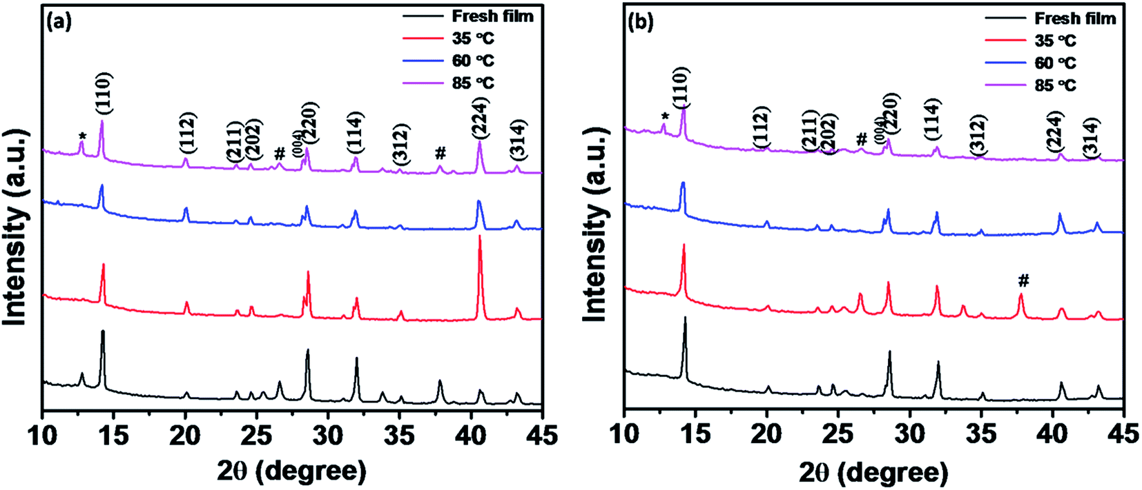 | ||
| Fig. 7 XRD pattern of (a) MAPbI3/p-TiO2 and (b) MAPbI3/m-TiO2 treated at constant RH of 85% at 35 °C, 60 °C and 85 °C for 6 h each. * – PbI2, # – FTO. | ||
The lower absorbance of the fresh film in Fig. 6(i) can be attributed to the transparent film quality as can be seen in its photographic image shown in Fig. 1. However, freshly grown SC-MAPbI3/m-TiO2 showed better absorbance compared to the MAPbI3/p-TiO2 films in the 500 to 750 nm range, as shown in Fig. 6(j). The superior absorbance is due to the large number of nucleation sites available for slow crystallization and dense crystal growth on the mesoporous substrate compared to the planar substrate.
To check for the presence of PbI2, which is the most commonly identified product on degradation of MAPbI3, XRD characterization was done on the fresh and aged films, and its corresponding patterns are given in Fig. 7. In Fig. 7(a), freshly grown MAPbI3/p-TiO2 film showed a small peak of unconverted PbI2 at 12.6° corresponding to (001) plane21 apart from the MAPbI3 peaks indicating that the fresh film itself did not crystallize homogeneously. In Fig. 7(b), the MAPbI3/m-TiO2 fresh films showed intense peak at 14.1°,which is the characteristic reflection from (110) plane of MAPbI3.29–31 No trace of PbI2 is found indicating full conversion of the reactants. As the films are exposed to the stressing environment, i.e., upon increasing the temperature to 35 °C and 60 °C at constant RH of 85%, the films in both cases showed minimal traces of degradation with only diminishing peak intensities of the perovskite phase. The early stage of degradation in perovskite phases which is mostly undetectable in XRD can be discerned from the absorbance spectra and surface morphological changes observed from the SEM images as depicted in Fig. 6. At extreme conditions of exposures, i.e. temperature kept at 85 °C and humidity maintained at 85% RH, a small XRD peak of PbI2 begins to show up in the films fabricated on both planar and mesoporous TiO2. These studies thus clearly bring out the quality of films and their endurance on the extreme temperature and humidity.
Conclusions
In summary, single crystalline perovskite films are successfully grown on planar and mesoporous TiO2 substrates. Uniform and dense films grew on the mesoporous TiO2 substrates compared to the planar TiO2 electrodes due to the better interfacial area available for nucleation. The influence of the underneath TiO2 layer on the device performance and stability is found to be very crucial. The SC-MAPbI3 film developed on m-TiO2 without a hole transporting material exhibited a promising efficiency of 3.2% on an active area of 0.3 cm2, whereas a PCE of 0.7% is obtained for the planar device. Moreover, the mesoporous devices are found to be more stable than the planar devices, with 70% retention of their initial PCEs for more than 5000 h. This can be owed to the resilience of the mesoporous architecture towards performance losses arising from ion vacancy migration compared to the planar architecture. As there is no considerable degradation in the films in ambient conditions even after 5000 h of exposure, the effect of extreme temperature and humidity on SC-MAPbI3 absorber material to degradation is investigated with respect to planar and mesoporous structure. It was observed that the films are stable even at 85 °C and 85% RH with only a slight detection of PbI2. This establishes the robust nature of the single crystalline films. However, the mechanism of its degradation is yet to be completely understood as we could not find notable difference in the structural degradation with respect to the underneath TiO2 layer when subjected to high stressing conditions. We conclude that the mesoporous template is the key for uniform growth, optimum device performance and stability of the SC-MAPbI3 films. By carefully controlling the film growth parameters such as temperature, precursor concentration and surface roughness, better quality SC-MAPbI3 films can be developed, which would further boost the performance.Conflicts of interest
There are no conflicts to declare.Acknowledgements
The authors are grateful to Technical Research Centre project (AI/1/65/ARCI/2014) and Clean Energy Research Initiative (DST/TMD/CERI/C247(G)), Department of Science & Technology, Government of India, for funding this work.References
- A. Kojima, K. Teshima, Y. Shirai and T. Miyasaka, J. Am. Chem. Soc., 2009, 131, 6050–6051 CrossRef CAS PubMed.
- Best Research-Cell Efficiency Chart|Photovoltaic Research|NREL, https://www.nrel.gov/pv/cell-efficiency.html, accessed 5 August 2019 Search PubMed.
- Q. Wang, B. Chen, Y. Liu, Y. Deng, Y. Bai, Q. Dong and J. Huang, Energy Environ. Sci., 2017, 10, 516–522 RSC.
- N. Park, Adv. Energy Mater., 2020, 10, 1903106 CrossRef CAS.
- A. Gomez, S. Sanchez, M. Campoy-Quiles and A. Abate, Nano Energy, 2018, 45, 94–100 CrossRef CAS.
- Q. Sun, P. Fassl, D. Becker-Koch, A. Bausch, B. Rivkin, S. Bai, P. E. Hopkinson, H. J. Snaith and Y. Vaynzof, Adv. Energy Mater., 2017, 7, 1700977 CrossRef.
- X. Wang, W. Li, J. Liao and D. Kuang, Sol. RRL, 2019, 3, 1800294 CrossRef.
- Q. Dong, Y. Fang, Y. Shao, P. Mulligan, J. Qiu, L. Cao and J. Huang, Science, 2015, 347, 967–970 CrossRef CAS PubMed.
- Y. Liu, Z. Yang, D. Cui, X. Ren, J. Sun, X. Liu, J. Zhang, Q. Wei, H. Fan, F. Yu, X. Zhang, C. Zhao and S. F. Liu, Adv. Mater., 2015, 27, 5176–5183 CrossRef CAS PubMed.
- D. Shi, V. Adinolfi, R. Comin, M. Yuan, E. Alarousu, A. Buin, Y. Chen, S. Hoogland, A. Rothenberger, K. Katsiev, Y. Losovyj, X. Zhang, P. A. Dowben, O. F. Mohammed, E. H. Sargent and O. M. Bakr, Science, 2015, 347, 519–522 CrossRef CAS PubMed.
- H.-L. Yue, H.-H. Sung and F.-C. Chen, Adv. Electron. Mater., 2018, 4, 1700655 CrossRef.
- R. Babu, L. Giribabu and S. P. Singh, Cryst. Growth Des., 2018, 18, 2645–2664 CrossRef CAS.
- Y.-X. Chen, Q.-Q. Ge, Y. Shi, J. Liu, D.-J. Xue, J.-Y. Ma, J. Ding, H.-J. Yan, J.-S. Hu and L.-J. Wan, J. Am. Chem. Soc., 2016, 138, 16196–16199 CrossRef CAS PubMed.
- J. Zhao, G. Kong, S. Chen, Q. Li, B. Huang, Z. Liu, X. San, Y. Wang, C. Wang, Y. Zhen, H. Wen, P. Gao and J. Li, Sci. Bull., 2017, 62, 1173–1176 CrossRef CAS.
- Z. Chen, B. Turedi, A. Y. Alsalloum, C. Yang, X. Zheng, I. Gereige, A. AlSaggaf, O. F. Mohammed and O. M. Bakr, ACS Energy Lett, 2019, 4, 1258–1259 CrossRef CAS.
- A. Gagliardi and A. Abate, ACS Energy Lett, 2018, 3, 163–169 CrossRef CAS.
- J.-H. Im, I.-H. Jang, N. Pellet, M. Grätzel and N.-G. Park, Nat. Nanotechnol., 2014, 9, 927–932 CrossRef CAS PubMed.
- J. Schlipf, A. M. Askar, F. Pantle, B. D. Wiltshire, A. Sura, P. Schneider, L. Huber, K. Shankar and P. Müller-Buschbaum, Sci. Rep., 2018, 8, 4906 CrossRef PubMed.
- A. R. Pascoe, M. Yang, N. Kopidakis, K. Zhu, M. O. Reese, G. Rumbles, M. Fekete, N. W. Duffy and Y.-B. Cheng, Nano Energy, 2016, 22, 439–452 CrossRef CAS.
- Y. Wu, A. Islam, X. Yang, C. Qin, J. Liu, K. Zhang, W. Peng and L. Han, Energy Environ. Sci., 2014, 7, 2934–2938 RSC.
- Y. Fu, F. Meng, M. B. Rowley, B. J. Thompson, M. J. Shearer, D. Ma, R. J. Hamers, J. C. Wright and S. Jin, J. Am. Chem. Soc., 2015, 137, 5810–5818 CrossRef CAS PubMed.
- Y. Song, W. Bi, A. Wang, X. Liu, Y. Kang and Q. Dong, Nat. Commun., 2020, 11, 274 CrossRef CAS PubMed.
- Z. Chen, Q. Dong, Y. Liu, C. Bao, Y. Fang, Y. Lin, S. Tang, Q. Wang, X. Xiao, Y. Bai, Y. Deng and J. Huang, Nat. Commun., 2017, 8, 1890 CrossRef PubMed.
- J. Jiang, Z. Jin, F. Gao, J. Sun, Q. Wang and S. F. Liu, Adv. Sci., 2018, 5, 1800474 CrossRef PubMed.
- G. Han, T. M. Koh, S. S. Lim, T. W. Goh, X. Guo, S. W. Leow, R. Begum, T. C. Sum, N. Mathews and S. Mhaisalkar, ACS Appl. Mater. Interfaces, 2017, 9, 21292–21297 CrossRef CAS PubMed.
- Z. Zhu, V. G. Hadjiev, Y. Rong, R. Guo, B. Cao, Z. Tang, F. Qin, Y. Li, Y. Wang, F. Hao, S. Venkatesan, W. Li, S. Baldelli, A. M. Guloy, H. Fang, Y. Hu, Y. Yao, Z. Wang and J. Bao, Chem. Mater., 2016, 28, 7385–7393 CrossRef CAS.
- G. Grancini, V. D'Innocenzo, E. R. Dohner, N. Martino, A. R. Srimath Kandada, E. Mosconi, F. De Angelis, H. I. Karunadasa, E. T. Hoke and A. Petrozza, Chem. Sci., 2015, 6, 7305–7310 RSC.
- J. S. Manser, M. I. Saidaminov, J. A. Christians, O. M. Bakr and P. V. Kamat, Acc. Chem. Res., 2016, 49, 330–338 CrossRef CAS PubMed.
- J. Zhao, Y. Deng, H. Wei, X. Zheng, Z. Yu, Y. Shao, J. E. Shield and J. Huang, Sci. Adv., 2017, 3, eaao5616 CrossRef PubMed.
- F. Huang, Y. Dkhissi, W. Huang, M. Xiao, I. Benesperi, S. Rubanov, Y. Zhu, X. Lin, L. Jiang, Y. Zhou, A. Gray-Weale, J. Etheridge, C. R. McNeill, R. A. Caruso, U. Bach, L. Spiccia and Y.-B. Cheng, Nano Energy, 2014, 10, 10–18 CrossRef CAS.
- L. Lee, J. Baek, K. S. Park, Y.-E. Lee, N. K. Shrestha and M. M. Sung, Nat. Commun., 2017, 8, 15882 CrossRef CAS PubMed.
Footnote |
| † Electronic supplementary information (ESI) available. See DOI: 10.1039/d0ra05590e |
| This journal is © The Royal Society of Chemistry 2020 |