 Open Access Article
Direct measurement of K+ ion efflux from neuronal cells using a graphene-based ion sensitive field effect transistor†
Hongmei Li *a,
Kenneth B Walshb,
Ferhat Bayrama and
Goutam Koleya
aDepartment of Electrical and Computer Engineering, Clemson University, Clemson, USA. E-mail: hongmel@g.clemson.edu; gkoley@clemson.edu
bDepartment of Pharmacology, Physiology & Neuroscience, University of South Carolina, Columbia, USA
First published on 13th October 2020
Abstract
A graphene-based ion sensitive field effect transistor (GISFET) has been developed and investigated in terms of its ion sensing performance. The GISFET sensor was found to demonstrate a high detection sensitivity enabling direct measurement of K+ ion efflux from live cells. The sensing performance of the GISFET was directly compared to that of a commercial Si ISFET and very similar detection results were obtained, highlighting the promise of the GISFET sensor for ion-sensing applications. Additionally, fabrication of a GISFET array containing 25 devices using a CMOS compatible photolithographic process was demonstrated, which resulted in good uniformity across the array and high ion sensing properties of the devices, underlining their application potential for simultaneous multi-well testing with small sample volume.
Introduction
Cell-based ion efflux assays are essential in biomedical research and drug discovery processes as they provide primary insight into the activities of ion channels in the cell membrane when they respond to external stimuli. The ion channels play crucial roles in cellular homeostasis and various cellular functions such as, neuronal signal transduction, muscle contraction, cell secretion, enzyme activation, and gene transcription, all of which are of high physiological significance.1,2 Consequently, extensive cellular assays to determine ion channel characteristics are routinely performed in modern laboratories. The patch-clamp technique is generally considered to be the “gold standard” for investigating ion channel activities, due to its direct, real-time, and highly accurate measurement capability. However, its complex operating procedure and low throughput make it impractical for applications involving large scale and simultaneous ion efflux measurements.3 Further, its invasive nature limits the duration over which the measurements can be conducted for a given cell. Therefore, an ion-channel characterization technique that is easy to operate, non-invasive, and high throughput, is highly desirable.Among the various alternative cellular efflux measurement techniques investigated so far, ion sensitive field effect transistor (ISFET) based assays have evolved as one of the most promising, as they offer fast, simple, and non-invasive measurement capabilities. These assays do not suffer from the complicacies of competing techniques, namely, ligand binding4 or fluorescent dye usage,5 which requires a scintillation process and elimination of imaging artifacts, as ion channel activities are determined indirectly through image analyses. Also, ISFET fabrication is fully compatible with traditional photolithographic processes, which makes them suitable for high volume production, and array-based measurements for simultaneous multi-well and multi-functional assays. However, commercial Si-based ISFETs that are available in the market have significant reliability issues with a short useful lifetime of only several weeks. This is due to unintentional diffusion of ions through the permeable SiO2 layer, and accumulation at the SiO2/Si interface during sensor operation in aqueous media (with high ionic concentration), which subsequently causes an irreversible degradation in their sensing performance. This issue can be addressed by fabricating graphene-based ISFETs (GISFETs), which uses impervious graphene as the ion sensing layer, which is typically coated with an ion selective membrane (that prevents damage to the graphene layer itself). Due to its high carrier mobility and atomically thin nature, graphene has demonstrated excellent ionic sensitivity,6–9 making it very well suited for ion efflux measurements.
Fabrication and characterization of GISFET have been reported earlier by Li et al.,6 which exhibited high sensitivity, selectivity, and excellent performance even when fabricated on flexible PET substrate instead of regular SiO2/Si substrates. Very good repeatability and reliability in the sensing performance of the GISFETs were presented in that report, where the K+ ion sensitivity was found to be stable over a duration of two months, which is a clear improvement over Si-ISFETs. Although extensive characterization results from these GISFETs were reported for K+ ion detection using diluted KCl solution, its performance involving ionic efflux from live cells has never been demonstrated. In addition, the potential compatibility of the ISFET fabrication method with standard photolithographic processes was also not investigated.
In this work, we have presented, for the first time to our knowledge, direct measurement of cellular K+ ion efflux using graphene-based ISFETs, and have demonstrated photolithographic micro-GISFET sensor array fabrication and its performance characterization for the first time.
GISFET's bio application feasibility
GISFET device fabrication
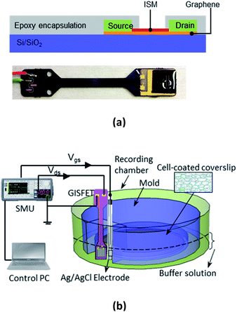
GISFETs were fabricated on SiO2/Si substrate with high quality graphene as the ion sensing layer. Graphene was synthesized using a home-built semi-automated CVD system on a copper foil (Alfa Aesar, 99.999% purity) at 1035 °C using CH4, H2, and Ar gases, following standard synthesis process developed in our lab.6,7,10 Following synthesis, a 1.5 × 3 mm graphene-on-copper foil was cut out of the large area sample to transfer the graphene onto a target SiO2/Si substrate. A solution based transfer process was followed using an initial PMMA coating on the graphene followed by treatment with ammonium persulfate to etch out the copper substrate. Details of the graphene transfer process have been described in earlier reports.6,11 Fig. 1(a) shows the GISFET layer structure and a picture of the fabricated GISFET. To form the source and drain contacts, Ti/Ni metal stacks were deposited on the graphene, using e-beam evaporator and a shadow mask, with 500 μm gap in between that constituted the channel of field effect transistor (FET). Then the graphene channel was spin-coated (film thickness of ∼5 μm) with K+ ion selective membrane (ISM), which gives the GISFET its ion selectivity. The ISM is based on a block copolymer with a two-phase system made of methyl methacrylate (MMA) and n-butyl acrylate (nBA) monomers. This two-phase system not only provides the membrane with a cross-linked stable structure from a crystalline phase (MMA), but also ensures rapid molecular transportation by a continuous amorphous phase (nBA).12 In this copolymer, valinomycin (C54H90N6O18) was dispersed to enable selective K+ ion capturing and transportation through the membrane. In addition, potassium tetrakis (4-chlorophenyl) borate (K-TCPB) was added to reduce the membrane resistance and activation barrier in ionic interfaces, which enabled the device to exhibit a higher ion-detection sensitivity.13,14 The fabricated ISFET device was mounted on a printed circuit board (PCB) to provide mechanical support for testing the GISFET. Finally, the PCB mounted sensor chip (with the fabricated ISFET) was encapsulated with biocompatible epoxy glue (Epo-tech 301) leaving a window open in the active sensing area (between ohmic contacts) to make sure the ions in the aqueous environment could reach the graphene surface.Device characterization and live-cell ion-efflux measurement set up
Electrical characterization of the ISFET was performed using a precision source measure unit (SMU, Keysight B2902A) by measuring its Id–Vd characteristics under different back gate biases, and Id–Vg for a fixed drain bias, using the highly doped n-Si substrate back gate biasing. This configuration can yield important parameters including graphene's mobility and carrier density. To characterize GISFET's sensing performance, a measurement setup was designed and assembled as shown in Fig. 1(b). In the recording chamber (17 mL culture well volume), a specially casted PDMS mold was placed to provide a space for cell-coated glass coverslip at the bottom of the well, as well as a notch where the GISFET device and a reference electrode could be inserted [see Fig. 1(b)]. This special geometry allowed the GISFET and a reference electrode to be as close to the cell coated surface as possible, minimizing the buffer solution volume dilution (which is important for accurate measurements of the K+ ion efflux from the cells). An Ag/AgCl (3 M NaCl) reference electrode was used to apply a constant voltage to the solution during measurements using the same SMU used to bias the ISFET.For sensing experiments, human U251-MG glioma cells were cultured in DMEM media supplemented with 10% fetal bovine serum (FBS), 50 U mL−1 penicillin, and 50 mg mL−1 streptomycin. Cells were plated on 25 mm coverslips in 12-well plates (50![[thin space (1/6-em)]](https://www.rsc.org/images/entities/char_2009.gif) 000 cells per well) for the GISFET measurements. Cells were stored in an incubator at 37 °C (5% O2/95% CO2) and used on days 2–3 after plating. The Ca2+ ionophore A23187 was used to activate Ca2+-activated K+ channels in the cells to initiate K+ ion efflux from the cells, which would increase the extracellular K+ concentration in the buffer solution (through a diffusion-based process), to be measured by the GISFET.
000 cells per well) for the GISFET measurements. Cells were stored in an incubator at 37 °C (5% O2/95% CO2) and used on days 2–3 after plating. The Ca2+ ionophore A23187 was used to activate Ca2+-activated K+ channels in the cells to initiate K+ ion efflux from the cells, which would increase the extracellular K+ concentration in the buffer solution (through a diffusion-based process), to be measured by the GISFET.
Graphene-based FET characterization
To determine graphene's electronic transport properties, the GISFET was first characterized in the air (optical image of the GISFET is shown as inset in Fig. 2). Fig. 2 shows the device's Ids–Vg (back-gate bias) measured with fixed drain-source bias (Vds) of 0.5 V. The curve presents a typical V-shaped characteristic of graphene drain current modulation as a function of back-gate bias, which is commonly observed.15 We find that as the back-gate bias is increased, the Ids drops at first, reaching a minimum value at Vg = ∼36 V (Dirac point), and then rises with further increase in the gate bias. The decrease in current with an increase in gate voltage indicates that the graphene (on SiO2/Si substrate) used in this work is p-type, which is also commonly observed due to the p-doping effect from SiO2 surface charge and affected by the wet transfer process.7,16 From the Ids–Vg plot, the field effect mobility can be calculated using the formula μFE = (gmL)/(WCoxVds), and was found to be 2560 cm2 V−1 s−1 (using capacitance per unit area Cox as 1.04 × 10⁻⁹ F, transconductance gm of 5.3 × 10⁻⁶ S, channel length L of 0.15 cm, and channel width W of 0.6 cm). The carrier density can then be determined as 8.3 × 1012 cm−2 from the equation p = σt/qμ = GL/(qμW), where G is conductance.6,17 Both the mobility and the carrier concentration are similar to those reported earlier.8,10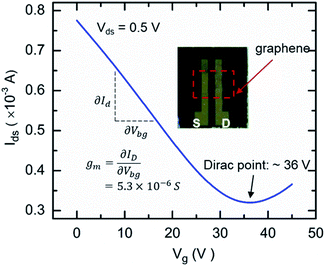 | ||
| Fig. 2 Electrical characterization of graphene FET device. Id–Vg measured from back-gated graphene FET in air shows typical V-shaped characteristic with a Dirac point of ∼36 V. | ||
GISFET characterization
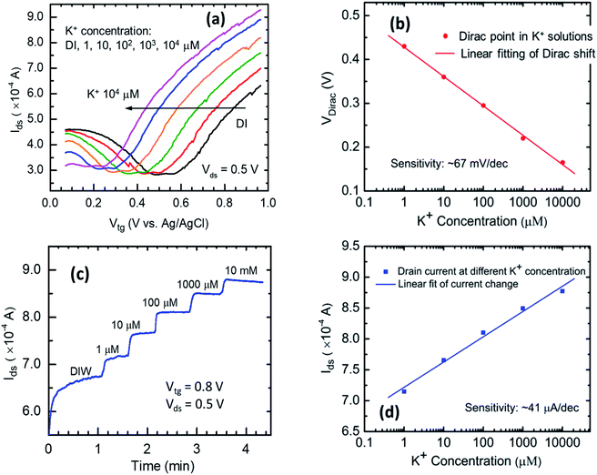
After GISFET fabrication, its ion sensing performance was first investigated in deionized (DI) water as the liquid medium, using two different methods, and the results are shown in Fig. 3. In the first method, we recorded shift in the GISFET's transfer characteristics (Ids–Vtg) shift (or Dirac point shift) responding to different K+ concentrations in the test medium. From Fig. 3(a), for a constant Vds of 0.5 V, the graphene's Dirac point can be observed to shift to the left as the K+ ion concentration increases. The ion concentration was increased by adding an appropriate amount of K+ stock solution to the DI water to attain concentrations of 1 μM, 10 μM, 100 μM, 1 mM, and finally to 10 mM, which resulted in a monotonic shift in the Dirac point by an overall magnitude of ∼270 mV. The value of Dirac point corresponding to each K+ ion concentration is plotted in semi-log scale in Fig. 3(b), which exhibits good linearity. From the least square fit line, the GISFET's ion sensitivity is calculated as 67 mV dec−1.In the other method, change in the GISFET's drain current as a result of ion concentration variation was investigated. A constant top-gate bias of 0.8 V and a drain bias of 0.5 V were applied to the device, and the drain current was recorded, while the ion concentration of the test medium was increased stepwise from 1 μM to 10 mM. The measurement results are shown in Fig. 3(c). We find that as the ion concentration increases, the drain current also increases in a stepwise fashion. The drain current corresponding to each ion concentration is plotted in a semi-log scale in Fig. 3(d). A nice linear variation is observed, and from the least square fit line, the sensitivity is calculated as 41 μA dec−1.
The measurement resolution for K+ ion concentration can be estimated from the drain current noise. The RMS noise was calculated from the flat steps of the drain current plotted in Fig. 3(c), for the same voltage bias before the K+ ion concentration is changed. The RMS noise is calculated as 0.4, 0.6, 0.7, 1.0, 2.3 μA for different concentration ranges, from which the resolution can be calculated as RMS/sensitivity (41 μA pK−1) = 0.01–0.05 per decade change in K+ ion concentration. From the drain current noise and the gm of the right-hand side section of the Id–Vtg plots in Fig. 3(a), the resolution can also be calculated for the first measurement method. Assuming the same drain current noise and the gm = 8.36 × 10⁻⁴ S, the VDirac noise can be calculated as 0.4–2.4 × 10⁻³ V. Then the resolution can be calculated to be 0.007–0.036 pK. Both the measurement methods (based on either change in Dirac point, or change in drain current) show high sensitivity to K+ ion concentration and high resolutions of ∼0.007 pK which is quite comparable to the resolution offered by commercial pH and pK (0.001–0.1 and 0.1, respectively) sensors.18–20
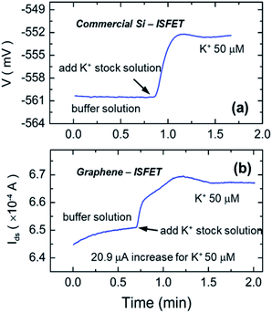
In addition to the investigation in DI water medium, the sensor's ion sensing performance was also examined in a NaCl buffer solution consisting of 140 mM NaCl, 1 mM CaCl2, and 1 mM MgCl2, which are at the levels present in the buffer solution used for cell culture.21 The measurements were carried out using the same set up shown in Fig. 1(b) to mimic the conditions of the live-cell assay conducted following these measurements. To benchmark the performance of our sensor, a commercial Si ISFET (D+T Microelectronica) was also used to record the response with K+ ion concentration variation. Fig. 4(a) and (b) compares Si-ISFET and GISFET's K+ ion sensing performance, respectively, in a physiological buffer solution containing a high concentration of different salts. Due to space restrictions in the measurement set up, the measurements using both sensors could not be performed simultaneously, but care was taken to keep the measurement conditions very similar for both measurements. Due to a different detecting scheme and circuitry, Si-ISFET displays changes in voltage while GISFET response is drain current change. After the two sensors were stabilized in the buffer solution in respective sensing experiments, K+ ion stock solution was pipetted in to raise K+ ion concentration from 0 to 50 μM. As a result, Si-ISFET showed a voltage increase by ∼8 mV of voltage, while the current in the GISFET increased by ∼21 μA. Percentage change in current was found to be ∼3.2% for our sensor compared to ∼1.4% change in voltage for the Si ISFET. A 50 μM K+ concentration change would correspond to a current change of 41 μA dec−1 × log![[thin space (1/6-em)]](https://www.rsc.org/images/entities/char_2009.gif) 50 = 69.5 μA change in current in DI, which is much larger than that actually observed for the buffer solution-based testing. The lower response is in line with typically observed reduction in sensitivity in physiological buffer solution compared to the DI water medium, and is also observed for Si ISFETS where the response was found to reduce from 60 mV dec−1 in DI water to 16.6 mV dec−1 in physiological buffer solution. Nonetheless, the response in the buffer solution serves as a reference to determine K+ ion concentration change resulting from cellular efflux caused by ion channel opening in live cells as discussed below.
50 = 69.5 μA change in current in DI, which is much larger than that actually observed for the buffer solution-based testing. The lower response is in line with typically observed reduction in sensitivity in physiological buffer solution compared to the DI water medium, and is also observed for Si ISFETS where the response was found to reduce from 60 mV dec−1 in DI water to 16.6 mV dec−1 in physiological buffer solution. Nonetheless, the response in the buffer solution serves as a reference to determine K+ ion concentration change resulting from cellular efflux caused by ion channel opening in live cells as discussed below.
Live-cell assay with GISFET ion sensor
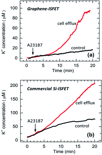
After investigating the GISFET's K+ sensing performance in DI water and physiological buffer solution, K+ ion efflux experiments from live-cells were carried out. A glass coverslip (25 mm diameter) with cultured U251 MG human glioma cells was placed at the bottom of the recording chamber containing 3 mL of physiological buffer solution. After ∼2 min of stabilization, a Ca2+ ionophore A23187 (1 μM) was pipetted into the solution through the notch formed at the side of the mold [see Fig. 1(b)]. The addition of A23187 stimulated a slow K+ efflux process from the cells, and the GISFET detected a rising K+ concentration for over 20 min in the buffer solution [see Fig. 5(a)]. From the current change of ∼25 μA and using the physiological buffer solution sensitivity of 12.3 μA dec−1 (obtained from Fig. 4(b), 20.9/(log![[thin space (1/6-em)]](https://www.rsc.org/images/entities/char_2009.gif) 50) μA dec−1), the K+ ion concentration increase due to cellular efflux was determined to be ∼100 μM over the 20 min duration as shown in Fig. 5(a). The observed transient response is very similar to that obtained with Si-ISFET test on live-cells [Fig. 5(b)] conducted in exactly the same way, as well as result reported in an earlier article by Walsh et al.21 However, we note that the K+ concentration change (the difference between the responses corresponding to cellular efflux and control) measured by the GISFET is almost 2 times lower than that estimated by the Si ISFET. We attribute this discrepancy to inaccuracies in the conversion factor (from a voltage or current change to K+ concentration) for the sensors.
50) μA dec−1), the K+ ion concentration increase due to cellular efflux was determined to be ∼100 μM over the 20 min duration as shown in Fig. 5(a). The observed transient response is very similar to that obtained with Si-ISFET test on live-cells [Fig. 5(b)] conducted in exactly the same way, as well as result reported in an earlier article by Walsh et al.21 However, we note that the K+ concentration change (the difference between the responses corresponding to cellular efflux and control) measured by the GISFET is almost 2 times lower than that estimated by the Si ISFET. We attribute this discrepancy to inaccuracies in the conversion factor (from a voltage or current change to K+ concentration) for the sensors.
Although successful measurement of ionic efflux from live cells demonstrates the feasibility of utilizing GISFET for various in situ biomedical measurements, however, for multiplexed and wide area sensing applications, the device needs to be fabricated in microscale so that much less volume of bio analytical sample is required for testing and spatial variations can be recorded. Additionally, the fabrication process should be compatible with current photolithographic processes for large scale production of sensors to reduce cost and variability, as well as, produce sensor arrays for multiplexed large area measurements needed for drug discovery. Such large area arrays would also be beneficial to investigate simultaneous cell behaviors over a large area by growing cells directly on the array, which can minimize ionic concentration dilution in the buffer solution. Thus, we fabricated GISFETs array using regular photolithographic microfabrication techniques and investigate their reliability and ion sensing performance.
GISFETs array and its characterization
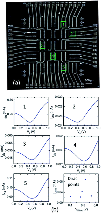
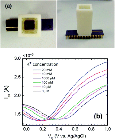
The G-ISFETs fabrication process introduced in the previous section used a shadow mask for source/drain patterning and a manual application of epoxy for encapsulation. The fabrication process was modified for utilizing photolithographic processes using a standard quartz photo-mask for patterning, graphene etch using an oxygen plasma etch chamber, and using patterned Su-8 for encapsulation of the device contacts. The fabrication step flow and optical microscopy images for each step are shown in Fig. S1 and S2,† respectively. Fig. 6(a) shows the optical image of a 5 × 5 GISFETs array fabricated over an area of 0.9 × 0.9 cm. To determine the quality and uniformity of the array, five GISFET devices were randomly chosen (marked in array chip image) and wire bonded to a 26 pin dual-in-line packaged (DIP) chip carrier. Their Ids–Vg characteristics were measured in DI water and are shown in Fig. 6(b) along with devices' Dirac points distribution. Each plot shows graphene's typical V-shaped Ids–Vg characteristic, while the plot of the Dirac points indicates confinement in a narrow range between 0.4–0.6 V, highlighting the excellent uniformity of the electrical characteristics of the device array.After inspection of basic electrical properties, the GISFET's ion sensing performance was investigated. For this, an analytical liquid reservoir was printed using a 3D printer (ZMorph 2.0 SX) and attached to the chip carrier chip with 1 × 1 cm solvent loading area. The top and side views of the DIP packaged GISFET array chip with the attached testing reservoir are shown in Fig. 7(a). A typical GISFET sensor's response to K+ ion concentration variation was measured and is shown in Fig. 7(b). K+ ion concentration was raised from minimal level (assumed ∼0 μM) to 20 mM, for the testing, which resulted in a Dirac point shift from 0.42 to 0.15 V. Based on the Dirac point shift, the sensitivity can be calculated as ∼63 mV dec−1, which is a very similar sensitivity to that observed for GISFETs fabricated manually (one device at a time) of ∼67 mV dec−1. The sensing performance of the single GISFET device shown in Fig. 3(c) and (d) was compared with the sensing performance of three devices in the GISFET array, and very similar percentage current change (∼27 ± 5%) was observed over the K+ ion concentration range of 1 μM to 10 mM for the 4 devices (shown in ESI Fig. S3†), which once again highlights the uniformity in the ISFET device sensing performance. Taken together, the fabrication uniformity and sensing results are very promising, and pave the way for future realization of larger arrays of graphene based GISFET devices for simultaneous multi-well testing with multiple analyte concentrations, or cellular efflux studies, with a small device footprint.
Conclusions
A highly sensitive GISFET sensor for K+ ion detection has developed with a high and stable sensitivity of ∼67 mV dec−1 or 41 μA dec−1. The GISFET sensor was utilized to directly measure K+ ion efflux from live neuronal glioma cells, and the results were found to be very comparable to those obtained using a commercial Si ISFET sensor. Design and fabrication of an integrated 5 × 5 GISFET array were carried out successfully, which displayed uniform characteristics among devices, as well as very good ion sensing performance. The high sensitivity and compatibility with standard photolithographic processing indicate that GISFETs can be a highly promising sensor for a wide range of biomedical sensing applications including multiplexed testing and multi-functional large area live cell-based assays.Conflicts of interest
There are no conflicts to declare.Acknowledgements
Financial support for this work from the National Science Foundation (Grants No. CBET-1606882, IIP-1602006, and EEC-1560070) is thankfully acknowledged. We also acknowledge Dr Swapan Ray at the University of South Carolina for generously supplying the Human U251-MG glioma cells used for testing.References
- J. E. Sirois and W. D. Atchison, Neurotoxicology, 1996, 17(1), 63 CAS.
- D. Häussinger, Biochem. J., 1996, 313(Pt 3), 697 CrossRef.
- W. Zheng, R. H. Spencer and L. Kiss, Assay Drug Dev. Technol., 2004, 2(5), 543 CrossRef CAS.
- D. S. Auld, M. W. Farmen, S. D. Kahl, A. Kriauciunas, K. L. McKnight, C. Montrose and J. R. Weidner, in Assay Guidance Manual, Eli Lilly & Company and the National Center for Advancing Translational Sciences, 2018 Search PubMed.
- W. Zheng, R. H. Spencer and L. Kiss, Assay Drug Dev. Technol., 2004, 2(5), 543 CrossRef CAS.
- H. Li, Y. Zhu, M. S. Islam, M. A. Rahman, K. B. Walsh and G. Koley, Sens. Actuators, B, 2017, 253, 759 CrossRef CAS.
- M. A. Uddin, Y. Zhu, A. Singh, H. Li, M. S. Islam and G. Koley, J. Phys. D: Appl. Phys., 2016, 49(46), 46LT02 CrossRef.
- H. Li, A. Singh, F. Bayram, A. S. Childress, A. M. Rao and G. Koley, Nanoscale, 2019, 11(23), 11145 RSC.
- S. Rumyantsev, G. Liu, M. S. Shur, R. A. Potyrailo and A. A. Balandin, Nano Lett., 2012, 12(5), 2294 CrossRef CAS.
- H. Li, X. Han, A. S. Childress, A. M. Rao and G. Koley, Phys. E, 2019, 107, 96 CrossRef CAS.
- H. Li, Graphene Based Ion Sensitive Field Effect Transistor for K+ Ion Sensing, PhD thesis, Clemson University, Clemson, 2020.
- R. He and T. Kyu, Macromolecules, 2016, 49(15), 5637 CrossRef CAS.
- C. C. Cid, J. Riu, A. Maroto and F. X. Rius, Analyst, 2008, 133, 1001 RSC.
- P. D. van der Wal, E. J. Sudhölter, B. A. Boukamp, H. J. Bouwmeester and D. N. Reinhoudt, J. Electroanal. Chem. Interfacial Electrochem., 1991, 317(1–2), 153 CrossRef CAS.
- Y. I. Zhang, L. Zhang and C. Zhou, Acc. Chem. Res., 2013, 46(10), 2329 CrossRef CAS.
- A. Singh, M. A. Uddin, T. Sudarshan and G. Koley, Small, 2014, 10(8), 1555 CrossRef CAS.
- A. K. Singh, M. A. Uddin, J. T. Tolson, H. Maire-Afeli, N. Sbrockey, G. S. Tompa, M. G. Spencer, T. Vogt, T. S. Sudarshan and G. Koley, Appl. Phys. Lett., 2013, 102(4), 043101 CrossRef.
- Thermo Fisher Scientific, Portable pH meters,https://www.fishersci.com/us/en/browse/90172045/portable-ph-meters.
- Thermo Fisher Scientific, Ion sensors, https://www.fishersci.com/us/en/catalog/search/products?keyword=ion+sensor.
- S. W. Bishnoi, C. J. Rozell, C. S. Levin, M. K. Gheith, B. R. Johnson, D. H. Johnson and N. J. Halas, Nano Lett., 2006, 6(8), 1687 CrossRef CAS.
- K. B. Walsh, N. DeRoller, Y. Zhu and G. Koley, Biosens. Bioelectron., 2014, 54, 448 CrossRef CAS.
Footnote |
| † Electronic supplementary information (ESI) available. See DOI: 10.1039/d0ra05222a |
| This journal is © The Royal Society of Chemistry 2020 |

