
 Open Access Article
 This Open Access Article is licensed under a Creative Commons Attribution-Non Commercial 3.0 Unported Licence
Synthesis and photoluminescence properties of hybrid 1D core–shell structured nanocomposites based on ZnO/polydopamine†
Viktoriia Fedorenko ac,
Roman Viter*ac,
Radosław Mrówczyńskib,
Daina Dambergaa,
Emerson Coyb and
Igor Iatsunskyi*b
ac,
Roman Viter*ac,
Radosław Mrówczyńskib,
Daina Dambergaa,
Emerson Coyb and
Igor Iatsunskyi*b
aInstitute of Atomic Physics and Spectroscopy, University of Latvia, Jelgavas 3, Riga, LV-1004, Latvia. E-mail: roman.viter@lu.lv
bNanoBioMedical Centre, Adam Mickiewicz University in Poznan, Wszechnicy Piastowskiej str. 3, 61-614 Poznan, Poland. E-mail: igoyat@amu.edu.pl
cCenter for Collective Use of Scientific Equipment, Sumy State University, 31, Sanatornaya St., 40018 Sumy, Ukraine
First published on 12th August 2020
Abstract
In the present work, we report on the modelling of processes at the zinc oxide and polydopamine (ZnO/PDA) interface. The PDA layer was deposited onto ZnO nanorods (NRs) via chemical bath deposition. The defect concentrations in ZnO before and after PDA deposition were calculated and analysed. The ZnONRs/PDA core–shell nanostructures were studied by transmission electron microscopy (TEM), X-ray diffraction (XRD), Raman and Fourier-transform infrared (FTIR) spectroscopy, photoluminescence (PL) measurements, and diffuse reflectance spectroscopy. The TEM and electron energy loss spectroscopy (EELS) measurements confirmed the conformal coating of PDA, while the PL emission from ZnO and ZnONRs/PDA samples showed a reduction of intensity after the PDA deposition. The decrease of defect concentration participating in PL and quantum efficiency explains the PL reduction. Finally, the observed decrease of activation energies and a shift of the PL peaks are attributed to the formation of an additional local electrical field between the PDA and ZnO nanostructures.
1 Introduction
Zinc oxide (ZnO) nanostructures are well known materials with advanced structural and optical properties.1–4 Due to their high refractive index, wide band gap and room temperature photoluminescence, they have been used in different applications, such as optical coatings, photocatalysis,5–8 optical sensors and biosensors.2,9,10 The electronic and optical properties of ZnO can be tuned by forming ZnO-composite nanomaterials.11–14 Metal nanoparticles that exhibit surface plasmon resonance (Au, Ag, etc.) and functional polymeric layers (polyaniline, polypyrrole, etc.)15,16 can be deposited on ZnO by chemical and physical methods.17,18 ZnO-composite nanomaterials have demonstrated tunable electronic and optical properties.15,16 Moreover, specific functional groups, for binding of different molecules, have been formed on the surface of ZnO-based nanocomposites, opening a broad range of applications, especially in biosensors.10,19–21The polymerization of functional polymers (polypyrrole, polyaniline, etc.) on ZnO surfaces requires special conditions, such as a low pH (2–3).22,23 However, it often results in the dissolution of ZnO template.24 Therefore, a possible solution is to use an additional redox agent for triggering polymerization at neutral pH or to deposit polymers, synthesized at higher pH (8–10). Among the polymers of interest, polydopamine (PDA) has a very attractive compound. PDA is a biocompatible material that has been used as a versatile coating and platform for biomedical application, drug delivery system preparation, sensors and biosensors, energy storage and batteries as well as photocatalysis.25–33 The advantage of PDA is its strong adhesive properties that allows to coat any surface both hydrophilic and hydrophobic. So far, PDA has been used to coat many materials i.e. alumina, silicon, magnetite, wood, glass, nanodiamonds and other carbon based materials.34–38 The crucial attribute allowing to use of the PDA in different applications is its biocompatibility, that has been proved under in vitro and in vivo conditions.39–44 Routinely, PDA is obtained by oxidative polymerization of dopamine in TRIS buffer at pH 8.5, which could be very promising for ZnO coating. PDA contains both quinone groups and an open-chain primary amine.45 The first one can be used to functionalized PDA with different moieties baring amino and thiol groups.46,47 The presence of primary amino group was confirmed by the diazotransfer reaction on PDA coated magnetic nanoparticles, which led to its further exploitation in organocatalysis.48,49 Importantly, it is suggested that amino and hydroxyl groups contribute to the adhesive properties of PDA.50
Indeed, it has been shown that the combination of PDA with ZnO can lead to enhanced performance in solar cells, optical coatings and antimicrobial materials.51–53 However, the mechanism of ZnO/PDA interfaces formation and its impact on optical properties has not been revealed yet. The main challenge regarding modelling of PDA/Semiconductor interfaces is the lack of consensus on the PDA structure. Up to this date, scientists are still debating about the final structure of the polymeric product of PDA, preventing for much needed Density Functional Theory (DFT) or other means for modelling the PDA/semiconductor interaction. Therefore, the use of spectroscopy methods is still the best tool available, in order to bring some understanding to the outstanding properties of PDA.25,54
Among the possible spectroscopy methods, photoluminescence (PL) is considered to be a powerful tool for analysis of metal oxide nanostructures.55 Among those oxides, ZnO have shown two emission bands: ultraviolet (free and bound excitons) and visible (vacancies and interstitials).56 Reshchikov et al. showed a methodology for the estimation of defect concentration in ZnO nanostructures by PL analysis.57,58 This method is based on the sublinear power dependence of defect PL intensity on the excitation power.57,58 As result, the defect concentration and quantum efficiency could be evaluated.57,58 Additionally, the activation energies and exciton binding energies in ZnO nanostructures could be evaluated from the temperature quenching of the PL spectra.57,58 Likewise, the activation energies and exciton binding energies provide important information on the photoinduced processes in ZnO and, more importantly, the role of bulk and surface contributions. Thus, PL is an ideal method for analysing ZnO/PDA nanocomposites, which can bring further insights on the interfacial phenomena occurring on these structures. Comparison of electronic (FTIR, Raman spectroscopy) and optical properties (PL emission) ZnO and ZnO–PDA nanostructures has never been studied before. Mechanisms of PDA layer forming on metal oxide surface and the role of ZnO defects on PDA structure are not revealed yet. Understanding of the above mentioned physical phenomena are important for further applications of PDA-based composites for sensor and biomedical purposes.
In this paper, we report on the analysis of the ZnO/PDA interface by low-temperature PL spectroscopy. The results allow to determine a correlation between the structural and optical properties of ZnONRs and ZnONRs/PDA nanostructures. Furthermore, the role of the PDA layer on PL emission intensity, defect concentrations and the quantum efficiency in ZnO/PDA nanostructures is analysed and discussed. Finally, the photoluminescence results, combined with Raman spectroscopy and FTIR data allow us to propose a model for forming of ZnO/PDA core–shell nanostructures. The results shown in this study provide a unique insight into the electronic process of the ZnO/PDA interface and shine a new light on the understanding of the interaction of PDA with oxide semiconductor surfaces.
2 Experimental section
2.1. Materials
Zinc acetate dehydrate, hexamethylenetetramine, 2-propanol (IPA), ethanolamine, sodium sulphate, zinc nitrate hexahydrate were obtained from Sigma Aldrich (Riga, Latvia), dopamine hydrochloride 99% (10174833), and tris(hydroxmethyl)aminomethane 99% (A18494) were purchased from Alfa Aesar (Poland), and were used without additional purification. The glass substrates (10 mm × 10 mm) were cleaned by successive sonication with deionized water and isopropyl alcohol for 10 min, with proper drying prior to final use. Oxygen plasma treatment for 15 min was performed in order to eliminate organic traces.2.2. Fabrication of ZnO nanorods
ZnO nanorods (ZnONRs) were deposited by hydro-thermochemical method (Fig. 1) as described in Viter et al. works.16,59 Initial ZnO seed layer has been prepared on glass by drop casting of 20 μL of 1 mg mL−1 zinc acetate methanol solution, followed by annealing at 350 °C for 1 hour. The glass substrates with ZnO seed layers were incubated for 4 hours in 50 mM of zinc nitrate and 50 mM of hexamethylenetetramine containing solution in water at 95 °C. A hydrothermal growth of ZnONRs was performed. The samples were washed by deionized water and dried at room temperature.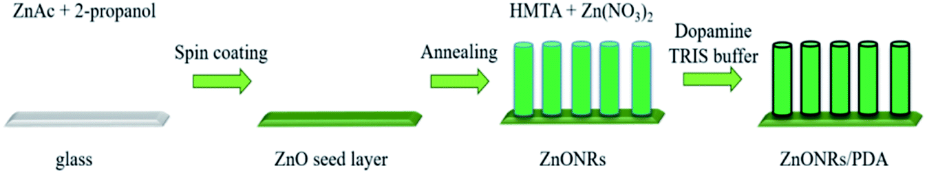 | ||
| Fig. 1 Schematic diagram of ZnONRs/PDA synthesis by combining hydrothermal method, and dopamine hydrochloride self-polymerization in alkaline aqueous solution. | ||
2.3. Deposition of polydopamine on ZnO nanorods
As deposited glass substrates (size 10 × 10 mm2) with ZnONRs were immersed into a Tris buffer (10 mM, pH 8.5, 50 mL) with a dopamine concentration of 0.4 mg mL−1 at room temperature for deposition time 2 hours. In the next step the samples were removed and rinsed with Milli-Q water and dried with nitrogen (N2) stream.2.4. Characterization
Structural properties of the ZnONRs–PDA nanostructures were investigated by XRD (PANAlytical Xpert-PRO diffractometer equipped with a Pixel 3D detector using Ni-filtered Cu Kα radiation 45 kV/40 mA), SEM (Zeiss Evo HD15 SEM from Zeiss Ltd (Jena, Germany)), HR-TEM (JEOL ARM 200F) high-resolution transmission electron microscope (200 kV) with EDX and EELS detector, Raman scattering measurements were performed using a Renishaw micro-Raman spectrometer equipped with a confocal microscope (Leica) and FTIR spectroscopy, using a FTIR-ATR spectrophotometer ‘Frontier’ from Perkin Elmer (Waltham, USA). Optical properties were studied by diffuse reflectance spectroscopy, using HR2000+ fiber spectrometer from Ocean Optics (Dunedin, USA). Low-temperature PL properties were studied by homemade setup (see ESI, Fig. S1†). The sample was assembled with copper holder into vacuum chamber with quartz window. Liquid nitrogen was injected into the cavity of the copper holder. The holder was equipped with K-type thermocouple, contacted the surface of the sample. The automatic temperature control was performed with precision of ±1 K. The measurements were performed with a step of 5 K. The PL was excited by Nd:YAG laser (266 nm, output power 29 mW) and collected by spectrometer Horiba iHR320. The measurements were performed in the range of 77–300 K.3 Results and discussion
The overall process for the synthesis of ZnONRs/PDA is shown in Fig. 1. In the first step glass substrate was covered with ZnONRs by hydro-thermochemical method according to previous report/according to protocol established in our laboratory (precise description is presented at experimental part).16Further obtained glass substrate with ZnONRs was coated with polydopamine using dopamine hydrochloride concentration of 0.4 mg mL−1 and time interval 2 hours in order to investigate its influence of optical properties of obtained material. This reaction was performed in Tris buffer at pH 8.5 allowing oxidative polymerization of dopamine.
The structural properties of obtained materials were characterized using X-ray diffraction (see Fig. 2a). In the presented diffractograms peaks located at 31.7°, 34.3°, 36.5°, 47.6°, 56.5°, 62.5° and 68.3° were assigned to (see Fig. 2a) ZnO wurtzite phase.56 In the XRD spectra of ZnONRs/PDA (see Fig. 2a) no significant changes on crystallinity can be found after the PDA coating, confirming the suitability of PDA for efficient coating of nanosurfaces. Morphology of the synthesized ZnONRs nanostructures was studied by SEM (see Fig. 2b). The diameter of the structures was found to be 50 ± 10 nm, and the length was about 550 ± 50 nm.
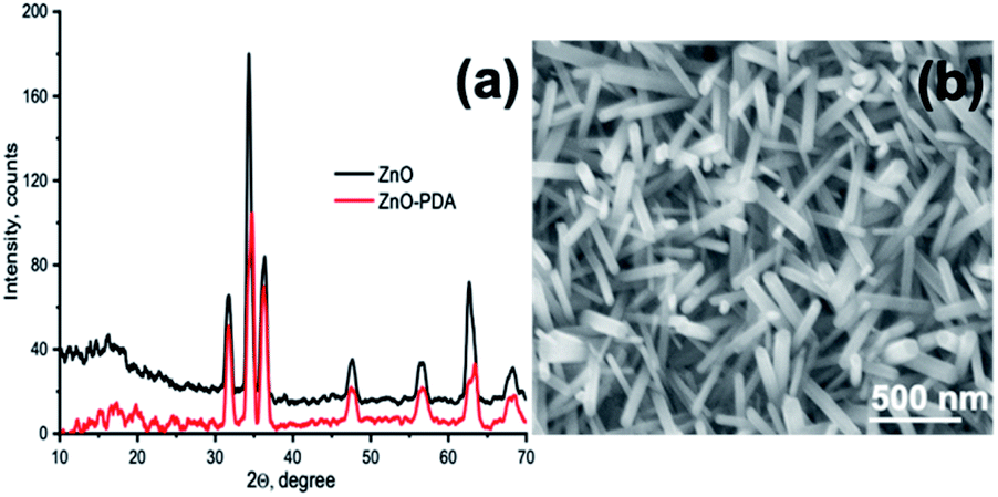 | ||
| Fig. 2 (a) XRD spectra of ZnONRs and ZnONRs/PDA; (b) SEM image of ZnONRs. | ||
The morphology and integrity of the PDA coating on ZnONRs was investigated by TEM (see Fig. 3a and b). These analyses revealed that ZnONRs were uniformly coated with a PDA layer with an average thickness less of ∼5 nm. Furthermore, electron energy loss spectroscopy (EELS) analysis on the ZnONRs, proved the presence of nitrogen, carbon, and oxygen, what indicated the formation of PDA in ZnONRs/PDA nanocomposite and confirmed the homogenous coating of ZnONRs. Moreover, since no visible structural changes or degradation of ZnONRs were observed, the deposit condition of PDA required no further optimization.
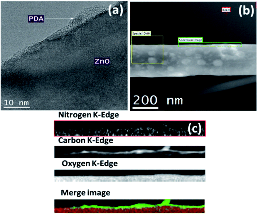 | ||
| Fig. 3 TEM images of ZnONRs/PDA: (a), and (b); electron energy loss spectroscopy (EELS) analysis of ZnONRs/PDA (c). | ||
In order to determine the composition of the produced nanocomposites, Raman spectroscopy was also used.60 Raman spectra of ZnONRs, PDA and ZnONRs–PDA are shown in Fig. 4a. As prepared ZnONRs showed peaks at 333, 376, and 435 cm−1, related to Ehigh2–Elow2 mode, A1(TO) polar optical phonon mode, and E2 (high) non-polar mode, respectively.61 The observed peak at 435 cm−1 (Ehigh2 mode) corresponds to the wurtzite phase of ZnO, as it was also confirmed by XRD. This mode is associated with the vibration of oxygen atoms in the crystal lattice. Raman peak at 586 cm−1 could be related to structural disorders (such as oxygen vacancies, Zn interstitial etc.).62 The Raman spectrum of PDA shows two characteristic peaks: 1357 and 1576 cm−1, corresponding to aromatic rings of PDA (stretching and deformation).63,64
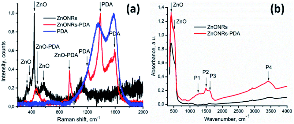 | ||
| Fig. 4 (a) Raman spectra of ZnONRs, PDA and ZnONRs–PDA; (b) FTIR of ZnO and ZnO–PDA nanocomposites. | ||
The ZnONRs–PDA nanostructures showed peaks at 466, 587, 954, 1214, 1386, 1596 cm−1. Raman peaks at 1386 and 1596 cm−1 correspond to PDA, and arise from the aromatic C–N stretching mode of the indole structure, and from the C![[double bond, length as m-dash]](https://www.rsc.org/images/entities/char_e001.gif) C aromatic ring vibration, respectively.65 The results thus confirm the successful deposition of PDA over ZnONRs surface.
C aromatic ring vibration, respectively.65 The results thus confirm the successful deposition of PDA over ZnONRs surface.
Wide peaks at 466 cm−1 and 1596 cm−1 were deconvoluted in two components via Lorentzian fitting. The resulting peaks showed the next values: 457 cm−1, 482 cm−1, 1525 cm−1 and 1596 cm−1. The analysis showed good agreement with the present peaks – 1206 cm−1, 1528 cm−1 and 1595 cm−1, and 1386 cm−1 with the PDA Raman modes, which related to C–OH or/and C–O, CC, C–N, N–H and CO vibrations, respectively.65 Finally, the peak at 457 cm−1 relates to ZnO, whereas peaks at 482 cm−1 and 954 cm−1 correspond to Zn–OH and O–H out-of-plane deformation mode.
FTIR spectroscopy was used to identify of functional groups present on synthesized materials (see Fig. 4b). The peak at 400 cm−1 and 560 cm−1 was attributed to ZnO vibrational modes. The peaks located at 1288 cm−1, 1492 cm−1, 1607 cm−1, and 3362 cm−1 corresponded to C–O, CN or/and CC, CO and –OH or/and N–H vibrational modes, respectively, these modes are in agreement with previously date for PDA.66 It is important to mention that the formation of PDA layer around ZnO leads to shift the FTIR peak positions of 12–20 cm−1 to lower values of wavenumbers.
Optical properties of the ZnO/PDA nanocomposites are not studied well. Due to conformal coating of the PDA over ZnONRs, changes in excitonic and defect emission of ZnONR photoluminescence are expected. We assume that ZnO–PDA interaction might involve ZnO defects. Defect concentration and their type affect optical and electronic properties of ZnO. Therefore, comparison of defect and excitonic parameters in ZnONR and ZnONR–PDA composites will clarify mechanisms of forming the composites. Thus, analysis of PL properties of ZnONRs and ZnONRs/PDA has been performed.
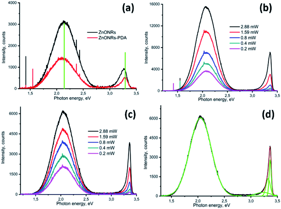
As already mentioned, PL is a simple method for surface defects characterization.2,13,67 Moreover, the emission vs. excitation power allows to evaluate the defect concentration and the quantum efficiency.2,13,68 The room temperature PL spectra of ZnONRs–PDA showed decrease of intensity and peak shift of ZnO after deposition of PDA layer (see Fig. 5a). We assume two possible mechanisms of the change in ZnONR–PDA PL spectrum: optical absorption by PDA layer and change of emission parameters of ZnO PL (decrease of emission centres concentration, increase of depletion layer, etc.).
 | ||
| Fig. 5 PL spectra of ZnONRs and ZnONRs–PDA at room temperature (a); ZnONRs (b) and ZnONRs–PDA (c) at 77 K, power dependence; deconvolution of the PL spectrum of ZnONRs–PDA (d). | ||
It was shown correlation between deposition time and PDA layer thickness.69 Deposition time of 24 hours produced PDA layers with thickness of 70–100 nm. One our deposition of PDA increased layer increase optical density approximately to 0.02 for the whole spectra in the range of 300–800 nm.69 No characteristic peaks were found. Based on calculation of the thickness of PDA layer and optical absorption we can assume about 6–7% of light absorption by PDA layer in ZnO NR–PDA nanostructure. This optical absorption doesn't explain drastic decrease of ZnONR–PDA PL emission and peak shift. Therefore, a reduction of PL intensity after the PDA deposition could be explained due to the decrease of defect concentration and change of depletion layer on the interface ZnO–PDA. In order to analyse these mechanisms, low temperature measurements of PL of ZnONR and ZnONR–PDA were analysed.
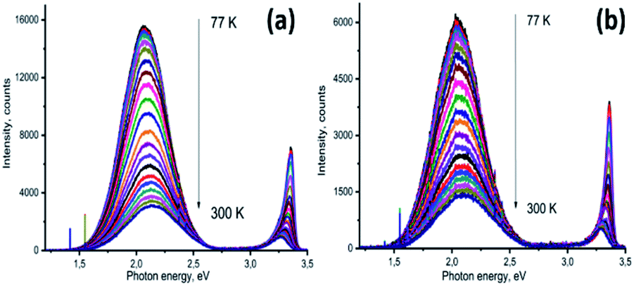
Influence of excitation laser power on PL emission of ZnONRs and ZnONRs–PDA nanostructures was investigated at 77 K (see Fig. 5b and c). Different excitation laser powers were achieved by using neutral filters. The decrease of excitation power resulted in decrease of the PL intensity (Fig. 5b and c). UV emission intensity decreased more drastically, compared to the visible emission. It points to different nature of emission mechanisms.67
Previously, we have shown analysis of the ZnO PL spectra and calculations of emission parameters (quantum efficiency and defect concentration).67 Due to complex behaviour of ZnO emission deconvolution of the emission spectra on separate emission peaks by using Gaussian function is required.67 The deconvolution of the PL spectrum of ZnO–PDA (Fig. 5 d) showed peaks, located at 2.05, 3.27, 3.348, 3.368 eV. The peaks, located at 3.27–3.368 eV and 2.05 eV were related to exciton and defect emission, respectively.70 It was found that excitation power dependence of the integrated intensity at 77 K showed sublinear dependence for peaks in the visible range and a superliner dependence for the UV peaks (see Table S1, ESI†). It is known that defects in ZnO are the source of charge carriers, charge traps and emission centres (centres of PL).67,71,72
To simplify calculations, we assume that only one emission centre is presented in the forbidden zone of ZnO and the absence of electron and hole traps (Fig. 6a). In this case, the dynamic equation of trapped and free electron concentrations will be described by the following kinetic equations:73
 | (1) |
 | (2) |
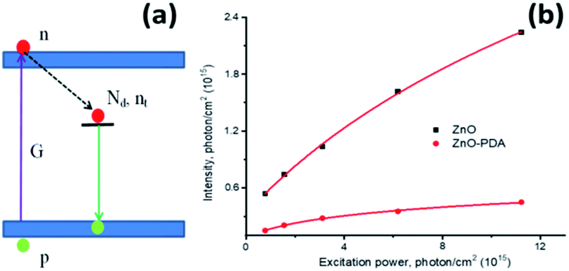 | ||
| Fig. 6 Diagram of possible radiative and nonradiative transitions (a). The power dependences of integrated intensities for ZnO and ZnO–PDA (b). | ||
Solving the eqn (1) and (2), the following expression for the emission intensity will be obtained:73
 | (3) |
The power dependences of integrated intensities for ZnONRs and ZnONRs–PDA, replotted in photon per cm2 are shown in Fig. 6b. The fitting of the curves gave following values for the defect concentration and quantum efficiency: 1.5 × 1015 cm−3 and 0.28 and 1.2 × 1014 cm−3 and 0.12 for ZnONRs and ZnONRs–PDA, respectively.
Low-temperature PL provides valuable information on the quenching of the emission mechanism of the system. Temperature dependence of PL for ZnONRs and ZnONRs–PDA in the temperature range 77–300 K are presented in Fig. 7a and b. Two effects were observed in both ZnONR and ZnONR–PDA nanostructures: temperature quenching of the PL and shift of the peaks. The increase of the temperature resulted in red shift of PL peak in UV region and blue shift of the visible emission. The effects of the peak shift have been previously discussed.58,67,74–76 Change of UV peak position is related to temperature dependence of ZnO band gap and transitions between bound and free excitons.67 Temperature range of this paper (77–300 K) is too high for existence of the bound excitons. As the ZnO band gap continuously decreases with temperature the shift of exciton emission towards lower values is followed.67
 | ||
| Fig. 7 Photoluminescence temperature dependence of ZnONRs (a) and ZnONRs–PDA (b). | ||
The increase of the temperature increases the lattice vibrations.67,75,76 In a number of reports the blue shift of visible emission was explained by electron-phonon coupling.67,75,76 The phonon coupling resulted in increase of the emitted photon energy.
Temperature quenching of photoluminescence provides information about activation energies and exciton binding energies.67 The following equation was used for the evaluation of ZnO and ZnO/PDA activation energy of PL quenching:74
 | (4) |
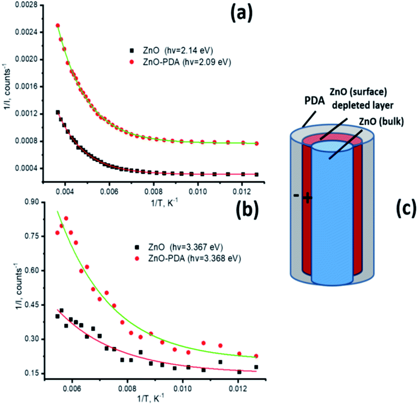 | ||
| Fig. 8 Exponential approximation for activation energy calculations (a and b). The model of forming ZnO/PDA interface (c). | ||
| 2.14–2.09 eV | 3.28–3.27 eV | 3.34–3.33 eV | 3.367 eV | |
|---|---|---|---|---|
| ZnO | 0.074 | 0.018 | 0.024 | 0.053 |
| ZnO–PDA | 0.064 | 0.01 | 0.013 | 0.044 |
Following model of forming ZnO/PDA interface is proposed. The model scheme of ZnO/PDA nanostructure is represented in Fig. 8c. Based on FTIR and Raman analysis, we assume that PDA is attached to the ZnO via –OH groups in PDA structure. Based on PL analysis, the intensity of the peaks and the defect concentration decreased after deposition of PDA over ZnONRs. Forming of ZnO/PDA interface involves ZnO defects, particularly doubly ionized oxygen vacancies/or oxygen interstitials. It is assumed that forming of ZnO/PDA interface decrease the concentration of ZnO defects. Due to new surface states, the local electrical field is formed increasing the depletion layer of ZnO. Forming of the additional local field results in a decrease of activation energies and shift of the PL peaks. Previously, it was shown that PL intensity is modulated by the value of the depleted layer in ZnO.71 Taking into account that the value of depleted layer is proportional to the Debye length, we assume that changes of the Debye length will affect the PL intensity. The Debye length can be estimated as:71
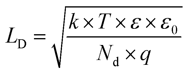 | (5) |
The proposed mechanism of PL quenching, proposed for ZnONR–PDA nanostructures here could be spread to other materials and composites where the depleted layer modulation is presented. Taking into account that the depleted layer may be changed under different external factors (e.g. adsorption of molecules; external coverage; heterojunction formation; material irradiation etc.), the proposed mechanism could also explained the principal of operation of (bio)sensors and detectors.
4 Conclusions
In summary, we have represented a comprehensive modelling of the processes on ZnO/PDA interface. The defect concentrations in ZnO before and after PDA deposition were calculated and analysed and decrease of concentration of defects, participating in PL and quantum efficiency was shown. The correlation between structural and optical properties of ZnO/PDA nanostructures was evaluated. TEM results demonstrated the ability to produce conformal PDA coating over ZnO nanorods. Change of FTIR and Raman spectra, due to the formation of ZnO/PDA composite suggest that PDA is attached to the ZnO via –OH groups in PDA structure. Defect levels of ZnO (oxygen vacancies) are involved in forming ZnO–PDA interface. Interaction of the defect levels with hydroxyl groups causes a decrease of the defect concentration, PL intensity and quantum efficiency. A decrease of activation energies and shift of the PL peaks observed in ZnONR–PDA nanostructures is explained by formation of additional electrical local field between PDA and ZnO.Our studies show the applicability of PDA coatings for controlling and improving semiconductor surfaces. Moreover, the results here presented provide further insights on the electronic response of PDA/Semiconductor materials toward their many optical and electronic applications in sensors and catalysis.
Conflicts of interest
There are no conflicts to declare.Acknowledgements
V. F. would like to thank the financial support from the project ‘Investigation of photoinduced processes in one dimensional ZnO/polydopamine nanostructures’, within Latvian Post-doc program (1.1.1.2/VIAA/2/18/279). R. M is grateful for the he financial support of National Science Centre of Poland under research grant OPUS number UMO-2018/31/B/ST8/02460. R. V. acknowledges the financial support from the project ‘1D ZnO/Polidopamīna kodola čaulas nanostruktūru izstrāde ar uzlabotu jutību un uzlabotām struktūras, elektroniskajām un optiskajām īpašībām’, within Latvian LZP fund (Reg. N. LZP 2018/1-0394).References
- A. Tamashevski, Y. Harmaza, R. Viter, D. Jevdokimovs, R. Poplausks, E. Slobozhanina, L. Mikoliunaite, D. Erts, A. Ramanaviciene and A. Ramanavicius, Talanta, 2019, 200, 378–386 CrossRef CAS PubMed.
- R. Viter, M. Savchuk, N. Starodub, Z. Balevicius, S. Tumenas, A. Ramanaviciene, D. Jevdokimovs, D. Erts, I. Iatsunskyi and A. Ramanavicius, Sens. Actuators, B, 2019, 285, 601–606 CrossRef CAS.
- O. Graniel, V. Fedorenko, R. Viter, I. Iatsunskyi, G. Nowaczyk, M. Weber, K. Załęski, S. Jurga, V. Smyntyna and P. Miele, J. Mater. Sci. Eng. B, 2018, 236, 139–146 CrossRef.
- J. Theerthagiri, S. Sunitha, R. Senthil, P. Nithyadharseni, A. Madankumar, P. Arunachalam, T. Maiyalagan and H.-S. Kim, Nanotechnology, 2019, 30, 27 CrossRef PubMed.
- M. T. Man, J.-H. Kim, M. S. Jeong, A.-T. T. Do and H. S. Lee, J. Lumin., 2017, 185, 17–22 CrossRef CAS.
- C. B. Ong, L. Y. Ng and A. W. Mohammad, Renewable Sustainable Energy Rev., 2018, 81, 536–551 CrossRef CAS.
- A. Ramirez-Canon, M. Medina-Llamas, M. Vezzoli and D. Mattia, Phys. Chem. Chem. Phys., 2018, 20, 6648–6656 RSC.
- C. M. Taylor, A. Ramirez-Canon, J. Wenk and D. Mattia, J. Hazard. Mater., 2019, 120799 CrossRef CAS PubMed.
- A. Tamashevski, Y. Harmaza, R. Viter, L. Dubovskaya, E. Slobozhanina, I. Volotovski and A. Ubelis, Research of zinc oxide nanorods application as a platform for immune biosensors development, 2016 Search PubMed.
- A. Tereshchenko, M. Bechelany, R. Viter, V. Khranovskyy, V. Smyntyna, N. Starodub and R. Yakimova, Sens. Actuators, B, 2016, 229, 664–677 CrossRef CAS.
- O. Lupan, V. Postica, R. Adelung, F. Labat, I. Ciofini, U. Schürmann, L. Kienle, L. Chow, B. Viana and T. Pauporté, Phys. Status Solidi RRL, 2018, 12, 1700321 CrossRef.
- R. A. Gonçalves, A. L. d. O. F. Rossetto, D. J. Nogueira, D. S. Vicentini and W. G. Matias, Aquat. Toxicol., 2018, 197, 32–40 CrossRef PubMed.
- R. Viter, M. Savchuk, I. Iatsunskyi, Z. Pietralik, N. Starodub, N. Shpyrka, A. Ramanaviciene and A. Ramanavicius, Biosens. Bioelectron., 2018, 99, 237–243 CrossRef CAS PubMed.
- V. Myndrul and I. Iatsunskyi, Materials, 2019, 12, 2880 CrossRef CAS PubMed.
- M. Turemis, D. Zappi, M. T. Giardi, G. Basile, A. Ramanaviciene, A. Kapralovs, A. Ramanavicius and R. Viter, Talanta, 2020, 211, 120658 CrossRef CAS PubMed.
- R. Viter, K. Kunene, P. Genys, D. Jevdokimovs, D. Erts, A. Sutka, K. Bisetty, A. Viksna, A. Ramanaviciene and A. Ramanavicius, Macromol. Chem. Phys., 2020, 221, 1900232 CrossRef CAS.
- L. Su and N. Qin, Ceram. Int., 2015, 41, 2673–2679 CrossRef CAS.
- D. Ponnamma, J.-J. Cabibihan, M. Rajan, S. S. Pethaiah, K. Deshmukh, J. P. Gogoi, S. K. Pasha, M. B. Ahamed, J. Krishnegowda and B. Chandrashekar, Mater. Sci. Eng. C, 2019, 98, 1210–1240 CrossRef CAS PubMed.
- Z. Hatami, E. Ragheb, F. Jalali, M. A. Tabrizi and M. Shamsipur, Bioelectrochemistry, 2020, 133, 107458 CrossRef CAS PubMed.
- N. Muthuchamy, R. Atchudan, T. N. J. I. Edison, S. Perumal and Y. R. Lee, J. Electroanal. Chem., 2018, 816, 195–204 CrossRef CAS.
- T. Liu, Q. Zhao, Y. Xie, D. Jiang, Z. Chu and W. Jin, Biosens. Bioelectron., 2020, 156, 112145 CrossRef CAS PubMed.
- S. G. Dhole, S. A. Dake, T. A. Prajapati and S. N. Helambe, Procedia Manuf., 2018, 20, 127–134 CrossRef.
- M. Chougule, G. Khuspe, S. Sen and V. Patil, Appl. Nanosci., 2013, 3, 423–429 CrossRef CAS.
- J. Han, W. Qiu and W. Gao, J. Hazard. Mater., 2010, 178, 115–122 CrossRef CAS PubMed.
- J. H. Ryu, P. B. Messersmith and H. Lee, ACS Appl. Mater. Interfaces, 2018, 10, 7523–7540 CrossRef CAS PubMed.
- V. Ball, Front. Bioeng. Biotechnol., 2018, 6, 109 CrossRef PubMed.
- R. Mrówczyński, ACS Appl. Mater. Interfaces, 2017, 10, 7541–7561 CrossRef PubMed.
- K. Qu, Y. Wang, A. Vasileff, Y. Jiao, H. Chen and Y. Zheng, J. Mater. Chem. A, 2018, 6, 21827–21846 RSC.
- R. Pan, Z. Wang, R. Sun, J. Lindh, K. Edström, M. Strømme and L. Nyholm, J. Materiomics, 2019, 5, 204–213 CrossRef.
- Z. Wang, J. Li, F. Tang, J. Lin and Z. Jin, RSC Adv., 2017, 7, 23535–23542 RSC.
- W.-X. Mao, X.-J. Lin, W. Zhang, Z.-X. Chi, R.-W. Lyu, A.-M. Cao and L.-J. Wan, Chem. Commun., 2016, 52, 7122–7125 RSC.
- A. Sukeri, A. Arjunan and M. Bertotti, Electrochem. Commun., 2020, 110, 106622 CrossRef CAS.
- Y. Wang, Y. Jia, Y. Zhou, Y. Wang, G. Zheng, K. Dai, C. Liu and C. Shen, J. Mater. Chem. C, 2018, 6, 8160–8170 RSC.
- Z. Wang, M. Yang, Y. Cheng, J. Liu, B. Xiao, S. Chen, J. Huang, Q. Xie, G. Wu and H. Wu, Composites, Part A, 2019, 118, 302–311 CrossRef CAS.
- R. Wang, D. Feng, T. Chen, S. Chen and Y. Liu, J. Alloys Compd., 2020, 825, 154081 CrossRef CAS.
- G. Liu, Z. Lu, X. Zhu, X. Du, J. Hu, S. Chang, X. Li and Y. Liu, Sci. Rep., 2019, 9, 1–10 CrossRef PubMed.
- H.-p. Zhang, W. Han, J. Tavakoli, Y.-p. Zhang, X. Lin, X. Lu, Y. Ma and Y. Tang, Composites, Part A, 2019, 116, 62–71 CrossRef CAS.
- J. C. Zuaznabar-Gardona and A. Fragoso, Sens. Actuators, B, 2018, 273, 664–671 CrossRef CAS.
- H. Lee, S. M. Dellatore, W. M. Miller and P. B. Messersmith, Science, 2007, 318, 426–430 CrossRef CAS PubMed.
- J. H. Cho, V. Vasagar, K. Shanmuganathan, A. R. Jones, S. Nazarenko and C. J. Ellison, Chem. Mater., 2015, 27, 6784–6790 CrossRef CAS.
- M. Martín, P. Salazar, R. Villalonga, S. Campuzano, J. M. Pingarrón and J. L. González-Mora, J. Mater. Chem. B, 2014, 2, 739–746 RSC.
- D. Maziukiewicz, B. F. Grześkowiak, E. Coy, S. Jurga and R. Mrówczyński, Biomimetics, 2019, 4, 3 CrossRef CAS PubMed.
- A. Woźniak, M. Walawender, D. Tempka, E. Coy, K. Załęski, B. F. Grześkowiak and R. Mrówczyński, Toxicol. in Vitro, 2017, 44, 256–265 CrossRef PubMed.
- X. Liu, J. Cao, H. Li, J. Li, Q. Jin, K. Ren and J. Ji, ACS Nano, 2013, 7, 9384–9395 CrossRef CAS PubMed.
- J. r. Liebscher, R. Mrówczyński, H. A. Scheidt, C. Filip, N. D. Hădade, R. Turcu, A. Bende and S. Beck, Langmuir, 2013, 29, 10539–10548 CrossRef CAS PubMed.
- J. Liebscher, Eur. J. Org. Chem., 2019, 2019, 4976–4994 CrossRef CAS.
- R. Mrówczyński, R. Markiewicz and J. Liebscher, Polym. Int., 2016, 65, 1288–1299 CrossRef.
- R. Mrówczyński, A. Bunge and J. Liebscher, Chem.–Eur. J., 2014, 20, 8647–8653 CrossRef PubMed.
- R. Mrówczyński, L. Magerusan, R. Turcu and J. Liebscher, Polym. Chem., 2014, 5, 6593–6599 RSC.
- P. Kord Forooshani and B. P. Lee, J. Polym. Sci., Part A: Polym. Chem., 2017, 55, 9–33 CrossRef CAS PubMed.
- N. Ahmad, X. Zhang, S. Yang, D. Zhang, J. Wang, S. uz Zafar, Y. Li, Y. Zhang, S. Hussain and Z. Cheng, J. Mater. Chem. C, 2019, 7, 10795–10801 RSC.
- L. Ai, Y. Wang, G. Tao, P. Zhao, A. Umar, P. Wang and H. He, Molecules, 2019, 24, 503 CrossRef.
- Y. Yang and W. Hu, Talanta, 2017, 166, 141–147 CrossRef CAS.
- M. Cîrcu and C. Filip, Polym. Chem., 2018, 9, 3379–3387 RSC.
- R. Viter, K. Jekabsons, Z. Kalnina, N. Poletaev, S. Hsu and U. Riekstina, Nanotechnology, 2016, 27, 465101 CrossRef CAS.
- R. Viter, A. A. Chaaya, I. Iatsunskyi, G. Nowaczyk, K. Kovalevskis, D. Erts, P. Miele, V. Smyntyna and M. Bechelany, Nanotechnology, 2015, 26, 105501 CrossRef PubMed.
- M. Reshchikov, A. Usikov, H. Helava, Y. Makarov, V. Prozheeva, I. Makkonen, F. Tuomisto, J. Leach and K. Udwary, Sci. Rep., 2017, 7, 9297 CrossRef CAS.
- M. A. Reshchikov, A. A. Kvasov, M. F. Bishop, T. McMullen, A. Usikov, V. Soukhoveev and V. A. Dmitriev, Phys. Rev. B: Condens. Matter Mater. Phys., 2011, 84, 075212 CrossRef.
- A. Tamashevski, Y. Harmaza, E. Slobozhanina, R. Viter and I. Iatsunskyi, Molecules, 2020, 25, 3168 CrossRef CAS PubMed.
- I. Iatsunskyi, G. Nowaczyk, S. Jurga, V. Fedorenko, M. Pavlenko and V. Smyntyna, Optik, 2015, 126, 1650–1655 CrossRef CAS.
- I. Mihailova, V. Gerbreders, E. Tamanis, E. Sledevskis, R. Viter and P. Sarajevs, J. Non-Cryst. Solids, 2013, 377, 212–216 CrossRef CAS.
- R. Viter, V. Khranovskyy, N. Starodub, Y. Ogorodniichuk, S. Gevelyuk, Z. Gertnere, N. Poletaev, R. Yakimova, D. Erts and V. Smyntyna, IEEE Sens. J., 2014, 14, 2028–2034 CAS.
- G. Yeroslavsky, R. Lavi, A. Alishaev and S. Rahimipour, Langmuir, 2016, 32, 5201–5212 CrossRef CAS PubMed.
- X. Yu, H. Fan, Y. Liu, Z. Shi and Z. Jin, Langmuir, 2014, 30, 5497–5505 CrossRef CAS.
- D. Chen, Y. Mei, W. Hu and C. M. Li, Talanta, 2018, 182, 470–475 CrossRef CAS.
- H. Luo, C. Gu, W. Zheng, F. Dai, X. Wang and Z. Zheng, RSC Adv., 2015, 5, 13470–13477 RSC.
- D. Damberga, R. Viter, V. Fedorenko, I. Iatsunskyi, E. Coy, O. Graniel, S. b. Balme, P. Miele and M. Bechelany, J. Phys. Chem. C, 2020, 124, 9434–9441 CrossRef CAS.
- R. Viter, A. Tereshchenko, V. Smyntyna, J. Ogorodniichuk, N. Starodub, R. Yakimova, V. Khranovskyy and A. Ramanavicius, Sens. Actuators, B, 2017, 252, 95–102 CrossRef CAS.
- M. L. Alfieri, L. Panzella, S. L. Oscurato, M. Salvatore, R. Avolio, M. E. Errico, P. Maddalena, A. Napolitano and M. d'Ischia, Biomimetics, 2018, 3, 26 CrossRef CAS.
- A. Janotti and C. G. Van de Walle, Phys. Rev. B: Condens. Matter Mater. Phys., 2007, 76, 165202 CrossRef.
- R. Viter, I. Iatsunskyi, V. Fedorenko, S. Tumenas, Z. Balevicius, A. Ramanavicius, S. Balme, M. Kempiński, G. Nowaczyk and S. Jurga, J. Phys. Chem. C, 2016, 120, 5124–5132 CrossRef CAS.
- M. A. Reshchikov, X. Gu, B. Nemeth, J. Nause and H. Morkoç, MRS Online Proc. Libr., 2005, 892 Search PubMed.
- M. Reshchikov and R. Korotkov, Phys. Rev. B: Condens. Matter Mater. Phys., 2001, 64, 115205 CrossRef.
- M. A. Reshchikov and H. Morkoç, J. Appl. Phys., 2005, 97, 5–19 CrossRef.
- M. Reshchikov, J. Xie, B. Hertog and A. Osinsky, J. Appl. Phys., 2008, 103, 103514 CrossRef.
- M. Reshchikov, H. Morkoc, B. Nemeth, J. Nause, J. Xie, B. Hertog and A. Osinsky, Phys. B, 2007, 401, 358–361 CrossRef.
- W. Lin, D. Chen, J. Zhang, Z. Lin, J. Huang, W. Li, Y. Wang and F. Huang, Cryst. Growth Des., 2009, 9, 4378–4383 CrossRef CAS.
- D. C. Look, Superlattices Microstruct., 2007, 42, 284–289 CrossRef CAS.
- Z.-Q. Fang, B. Claflin, D. C. Look and G. C. Farlow, J. Appl. Phys., 2007, 101, 086106 CrossRef.
Footnote |
| † Electronic supplementary information (ESI) available. See DOI: 10.1039/d0ra04829a |
| This journal is © The Royal Society of Chemistry 2020 |