DOI:
10.1039/D0RA04763E
(Paper)
RSC Adv., 2020,
10, 26675-26685
Role of annealing temperature on optimizing the linear and nonlinear optical properties of As40Se50Ge10 films
Received
30th May 2020
, Accepted 9th July 2020
First published on 16th July 2020
Abstract
The present work shows the effect of annealing conditions on the linear and nonlinear optical properties of two-year-old thermally evaporated 800 nm As40Se50Ge10 thin films. The aging effect in this film is clearly noticeable as compared with the old observation. The two-year-old films were annealed at different temperatures like 373, 413, 453 and 493 K for 1 h. The optical parameters were calculated from the optical transmittance and reflectance spectra measured at normal incidence of light by spectrometer in the 500–1000 nm range. The linear refractive index (n) and extinction coefficient (k) were decreased with annealing temperature. The observation reveals the increase in optical band gap with increase in annealing temperature while the width of the tail in the gap has an opposite behaviour. The oscillator energy, dispersion energy, dielectric constant, the loss factor, and optical conductivity were discussed in detail. The nonlinear refractive index and optical susceptibility were calculated by using Miller's formula which decreased with annealing temperature. The changes in both linear and nonlinear optical parameters with annealing temperature showed that annealing temperature can be considered as a useful factor for controlling the optical properties of As40Se50Ge10 chalcogenide films which could be the candidate for numerous photonic applications. The structural study was done by X-ray diffraction and Raman spectroscopy.
1. Introduction
Chalcogenide thin films have attractive optical properties like linear and nonlinear refractive index, 3rd order optical susceptibility, broad range of transparency and low phonon energy.1,2 However, the nonlinear refractive index makes them play an important role in optical switching, light amplification, super continuum generation etc.3–5 The tuning of such optical properties of chalcogenide thin films can be done with various processes like doping of elements, thermal annealing, laser irradiation, ion irradiation, etc.6–10 Out of these techniques, thermal annealing is considered a simple way to bring about changes in the structural, optical and electrical properties in such types of materials. The surface morphology along with the interior of the material is being modified with temperature and time. Thermal annealing accelerates the relaxation of the film into its equilibrium state since the room temperature relaxation time for non-annealed films has been reported to be very high.11 Heat treatment or annealing is a more useful method to detect the changes in physical properties that are triggered by the structural relaxation in the materials.12
The chalcogenide materials show aging effect which is observed in its structural as well as optical parameters.13,14 The aging effect showed both photodarkening and photorefraction can be possible only in aged As–S–Se glasses while they are prevented in freshly annealed one.15 The physical aging becomes slower with year and it is very difficult to identify the completion of physical aging after long years.16 The main reason for the physical aging in chalcogenide materials is the thermodynamic instability and excess free enthalpy below their glass transition temperature (Tg). However, with time, the structure relaxes towards a more thermodynamically stable state.17,18 The aging process brings changes to the structural, mechanical, thermal and optical properties of glassy films thus understanding the aging process is essential to both fundamental glass science and practical applications involving glassy materials.19
The phenomenon of physical aging in chalcogenide glasses has attracted a substantial attention because of new prospects for chalcogenide-based optoelectronics.20 The reason is that chalcogenide obtained in thermodynamically nonequilibrium state as frozen supercooled liquid owing to conventional melt-quenching route21 aspire with time to a more energetically favourable state, changing their exploitation parameters. The optical property control of chalcogenide thin films is necessary for technological applications that requires a better understanding of their network structure. The assessment of a natural physical aging effect on their optical and morphological characteristics could be detrimental for a variety of optics and photonics applications. So, we have tried to observe the various changes in the 2 years old As40Se50Ge10 thin films due to aging process upon thermal annealing.
Coming to the importance of the material prospective, the As–Se–Ge system is having a wide range of glass formation that enables tuning of the properties of the materials over a wide range.22 For this unique property, As–Se–Ge based thin films are widely used in various acousto-optic devices,23 infrared transmitters, waveguides for supercontinuum generation24 and optical switching fibres.25 As–Se–Ge films showed good changes in optical band gap and refractive index on annealing.26 The As–Se–Ge films possess better photostability with zero photorefraction in the relaxed states.27 The Ge15As24.5Se60.5 film upon continuous illumination showed photoinduced effects which is used for waveguide fabrication.28 The optical nonlinearity in As–Se–Ge system is 100 to 1000 times more than of Si based glasses which is thus useful for optical components that have significant improvement in device performance.29 The 100 MeV Ag ion irradiation on As–Se–Ge system modified the structural as well as optical parameters which becomes useful candidate for optical components with low optical loss and ultra-fast optical response time.30 Also, the thin films of Ge–As–Se family have attracted considerable interest because of the changes in their structure and electronic properties observed under thermal treatment and illumination.31,32 In our previous report, we had shown the influence of Ge addition on the optical properties of As40Se50Ge10 thin films.33 However, the tuning of linear and non-linear optical constants in thermally evaporated As40Se50Ge10 film by annealing at different temperature including both below and above Tg is not yet investigated. The Tg for the As–Se–Ge system varies between 150 °C to 200 °C approximately with low value of Ge%.34 The nonlinear refractive index and 3rd order optical susceptibility tuning at different annealing temperature is being investigated in the present work.
The main aim of the present work is to measure the linear optical parameters (absorption coefficient, extinction coefficient, optical band gap, oscillator energy, dispersion energy, refractive index, optical conductivity) and nonlinear optical constants (3rd order optical susceptibility, nonlinear refractive index) etc. of As40Se50Ge10 thin film w. r. t the annealing temperature. The old thermally evaporated film was annealed at different temperatures such as 373 K, 413 K, 453 K (below Tg) and 493 K (above Tg) which were characterized by various experimental techniques. The single oscillator Wemple–DiDomenico model was utilized to evaluate the oscillator energy and the dispersion-energy. The important nonlinear parameters were evaluated by using the semi empirical Miller's formula using the linear parameters.
2. Experimental details
2.1. Sample preparation
Two years old thin films of As40Se50Ge10 with 800 nm thickness were annealed at different temperatures 373, 413, 453 and 493 K under vacuum of 10−3 torr respectively for 1 h. The thin film was deposited on glass substrate by thermal evaporation method using the Hind-High vacuum coating unit (HIND-HIVAC Model 12A4D) from bulk As40Se50Ge10 sample two years ago. The vacuum of the system was maintained at 5 × 10⁻⁵ torr and the glass substrate was maintained at room temperature by cooling system. The substrates were rotated very precisely during the deposition process to obtain a homogenous, uniform and smooth film. The crystal thickness monitor attached to the coating unit was used to measure the thickness of the film and the rate of deposition was kept at 0.5 nm s−1.
2.2. Characterizations techniques
The optical transmittance (T) and reflectance (R) spectra were recorded by the UV-Visible spectrometer (Bruker Optics (IFS66v/S) within the wavelength range 500–1000 nm. In the UV-Vis spectrometer, before starting the experiments, the reference samples (BaSO4) showed zero absorption which was carried out through the baseline correction and auto zero options available with the control software. The optical bandgap was calculated by using straight line fitting in the linear portion of the curve by origin software and the standard error was calculated from the fitting data by software itself with R value as 0.99. X-ray diffraction technique (Bruker D8 Advance) was used to examine the amorphous/crystallinity nature of aged and annealed films. The diffractometer has a Cu–Ni filter of Kα-radiation of wavelength 1.5418 Å. The measurements were taken at 40 mA current and 40 kV voltage with a scan speed of 1° min−1, a step value of 0.02° in 2θ range of 10°–80° at a grazing angle of 1°. Corundum was used as a reference in the XRD measurements before taking measurements of our samples. To ensure the presence of elements in the film, energy-dispersive X-ray spectroscopy (EDAX) was done for the films and attachment facility of the field emission scanning electron microscope (FESEM) was used to acquire the corresponding surface morphological picture. The scan was done at an accelerating voltage of 20 kV and 40 mA of emission current with sample exposure of 1 cm2 size at a pressure of 2 × 10⁻⁷ torr. The scan was taken at various positions 3–4 times in order to avoid the errors. To get more information regarding its structural data, Raman spectroscopy measurements were performed (LabRAM HR system) by the use of 514.5 nm argon laser with a CCD detector in backscattering mode in a range of 50–400 cm−1. The Raman spectra were calibrated using the 520 cm−1 line of silicon thin film. After calibration, 3–4 measurements were taken for the same sample at different positions for same time intervals (40 seconds) to minimize the systematic error.
3. Results and discussion
3.1. Linear optical properties
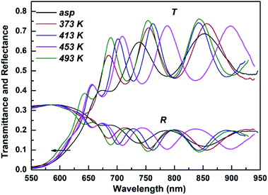
Transmittance (T) and reflectance (R). Fig. 1 represents the transmittance T(λ) and reflectance R(λ) spectra of the investigated films of As40Se50Ge10 at various annealing temperatures. It is clear from the spectra that these spectra could be divided into two main spectral regions (1) high absorption region of wavelength ≤ 675 nm (2) transparent region of wavelength ≥ 675 nm. The transmitting power measures the penetration of the electromagnetic waves inside the film that is useful for photonic applications. It is observed from Fig. 1 that the transmittance relatively increased for the annealed films as compared to the as-prepared aged film. The maximum transmittance for the as-prepared aged film is ∼68% which increases to a maximum value of ∼76% for the 493 K annealed film. The increase in transmittance is due to the reduction of surface scattering as seen from other studies.35,36 This also indicates the relaxation in the annealed films. The reflectance spectra showed opposite trend as that of the transmittance which is small in magnitude.
 |
| | Fig. 1 Transmittance and reflectance spectra of the studied films. | |
The systematic interference pattern at higher wavelength is due to interference between film surface and the substrate which indicates the homogeneity and smoothness of the films.37,38 The high absorption region shows the blue shift (towards lower wavelength/higher energy) that indicates the increase in bandgap with annealing.
3.2. Absorption coefficient (α)
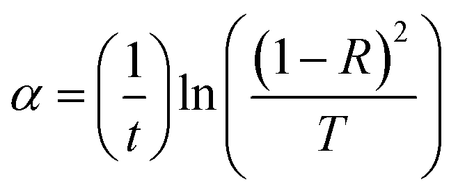
The optical absorption spectra are used to evaluate the absorption coefficient, optical bandgap, disorder parameter, band tail width and nature of transition involved in the film. The absorption edge refers to the split-up energy between the lowest of the conduction band and the highest of the valance band that gives the optical band gap. The transmittance, reflectance and thickness of the film are related to the absorption coefficient by the relation39,40which on simplification gives| |
 | (2) |
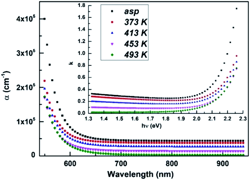
The increase in annealing temperature decreased the absorption co-efficient as shown in Fig. 2. The obtained absorption coefficient is of the order of 104–105 cm−1, which agrees well with the results reported by others and it decreased with wavelength. This indicates that after the absorption edge, the film becomes more transparent and the light wave can propagate faster and easier.
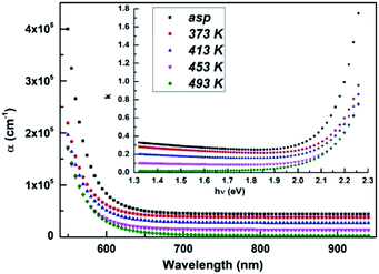 |
| | Fig. 2 Absorption and extinction coefficient of the studied films. | |
3.3. Extinction coefficient (k)
The extinction coefficient (k) of the studied films was calculated by using the relation involving absorption coefficient and wavelength41,42
The constant k represents the material ability for polarization is shown in Fig. 2 (inset). The k value increased with photon energy (hν) and decreased with annealing. The decrease of k is due to the decrease in carrier concentration43 and decrease in density of defect states as k is related to the surface defects and disorder.44
3.4. Optical band gap (Eg) and Tauc parameter (B1/2)
The optical energy gap (Eg) and nature of band transition was obtained in the high absorption region (α ≥ 104 cm−1) by Tauc relation45where B is a parameter that depends on the transition probability (Tauc parameter), h and ν are the Planck's constant and frequency of the incident photon. The value of ‘m’ determines the mechanism of optical absorption whose value is ½ for direct allowed transition and 2 for indirect allowed transition.46,47 The linear fitting of the data points of the linear portions by taking m = 2 shows the indirect allowed transition in the film. The plot of (αhν)1/2 vs. hν gives a straight line and the x intercept gives the optical band gap as shown in Fig. 3. The estimated values of Eg are presented in Table 1 which clearly shows the increased value for the annealed one as compared to the as-prepared one. The as-prepared Eg value (1.85 eV) is also more than that of the 2 year-old same film whose value was 1.66 eV.31 This clearly shows the aging effect on the studied As40Se50Ge10 film. The annealed film at 493 K possess Eg value of 1.97 eV which is 0.12 eV more than the as-prepared one. The systematic increase of Eg with annealing is a result of the decrease of defects which forms the localized states in the band gap according to Davis Mott model.48 The heat energy supplied to the film annealed out the defects by converting the homopolar bonds to heteropolar one thus reducing the defects and the degree of disorder.| |
 | (5) |
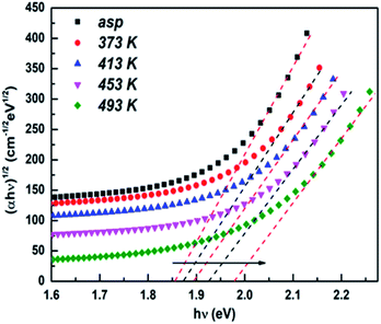 |
| | Fig. 3 Variation of (αhν)1/2 with hν for the studied films. | |
Table 1 Optical parameters of the studied films
| Sample As40Se50Ge10 |
Bandgap (Eg) in eV |
B1/2 in cm−1/2 eV−1/2 |
Urbach energy (eV) |
Eo (eV) |
Ed (eV) |
Oscillator strength (f) |
| As-prepared |
1.855 ± 0.001 |
418 ± 3 |
0.213 |
3.62 |
14.28 |
51.69 |
| 373 K |
1.872 ± 0.001 |
439 ± 2 |
0.201 |
3.71 |
15.24 |
56.54 |
| 413 K |
1.894 ± 0.001 |
464 ± 1 |
0.189 |
3.74 |
17.73 |
66.31 |
| 453 K |
1.925 ± 0.002 |
489 ± 2 |
0.164 |
3.82 |
18.27 |
69.79 |
| 493 K |
1.976 ± 0.002 |
517 ± 1 |
0.138 |
3.91 |
18.97 |
74.17 |
So, the reduction in the density of defects reduce the width of the localized states and thus increased the Eg for the annealed films like other studies.49,50
The measure of disorder (B1/2) value was obtained from the slope of the fitting in eqn (4). The Tauc parameter increased with annealing infers the decrease in disorder as B1/2 is inversely proportional to disorder.51
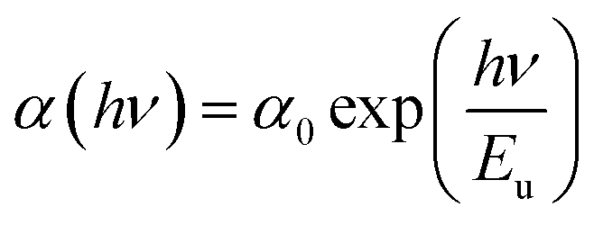
The absorption coefficient (α) in the lower absorption region depends exponentially on photon energy (hν) by Urbach relation.52| |
 | (6) |
where α0 is a constant, and α is the absorption coefficient, h is Planck's constant and Eu is the Urbach energy. By plotting a graph between ln(α/α0) on the y-axis vs. (hν) on the x-axis and then the straight-line fitting to the curve gives the slope as (1/Eu). The inverse of the slope gives the value of Urbach energy that represents the degree of disorder in amorphous materials.53 The calculated values are presented in Table 1 which shows that the Eu decreased with annealing temperature which infers to the decrease in defect states in the localized region. The decrease of Eu and increase of Eg with annealing temperature (Fig. 4) can be attributed to the decrease of the degree of disorder that results in the decrease of the band tailing, and consequently an increase of the band gap.9,54
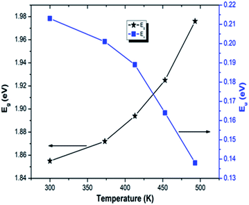 |
| | Fig. 4 Variation of Eg with Eu for the studied films. | |
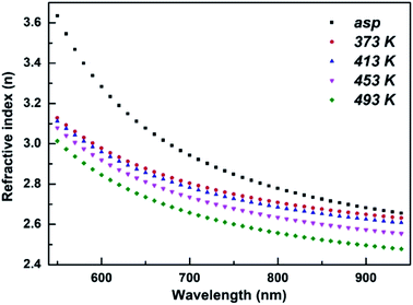
3.6. Linear refractive index (n)
The linear refractive index (n) was calculated from the transmittance and reflectance spectra by using inverse synthesis method55,56 as shown in Fig. 5. It is clear from the figure that n decreases with the increase of wavelength. This result is attributed to the decrease of absorption coefficient with wavelength indicating the normal dispersion behaviour of the studied films. In addition, the refractive index decreased with annealing temperature that proves the established Moss rule which states Egn4 ∼ constant.57 The increase in Eg value is accompanied by the decrease of refractive index.58
 |
| | Fig. 5 n vs. λ plot of the studied films. | |
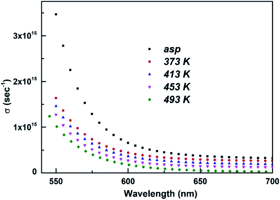
3.7. Optical conductivity (σopt)
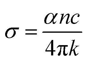
The optical conductivity (σopt) is an important parameter to get knowledge about the electronic state in the material with the help of absorption coefficient and refractive index.59 The optical conductivity of a material is expressed as,| |
 | (7) |
where α, n and k are the absorption coefficient, linear refractive index and extinction coefficient respectively. Fig. 6 shows the variation of the optical conductivity vs. wavelength for the as-prepared and annealed films. From the figure, one can infer that, the optical conductivity decreased with increasing wavelength and also decreased with increasing annealing temperature. The decrease in σopt with annealing is due to the decrease in absorption coefficient and decrease of localized states and defects by annealing temperature.60
 |
| | Fig. 6 Variation of σopt with λ at various annealing temperature. | |
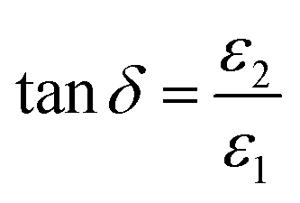
3.8. Dielectric constants and loss factor
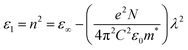
The complex dielectric constant (ε* = ε1 − iε2) is considered as an intrinsic property of the material which is to be determined to understand the optical properties. The real (ε1) and imaginary (ε2) part of the dielectric constant (ε*) are related to the optical constants as| | |
ε1 = n2 − k2 and ε2 = 2nk
| (8) |
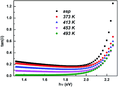
The real part represents the dispersion (how much the electromagnetic wave slows down) in the material whereas the imaginary part gives the dissipative rate of the wave (how a dielectric material absorbs energy from an electric field due to dipole motion).61,62 The variations of the dielectric constants ε1 and ε2 versus energy (hν) are shown in Fig. (7a and b). Both of ε1 and ε2 increases with the energy while they decrease with increasing annealing temperature. This behaviour is in accordance with the value of α and k. The ratio of imaginary part to real part gives information about the dissipation factor (tangent or loss factor) as given by
| |
 | (9) |
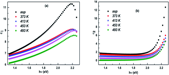 |
| | Fig. 7 The variation of (a) real (ε1) and (b) imaginary (ε2) parts of dielectric constant. | |
The dissipation factor tan(δ) measures the loss-rate of power of a mechanical mode, such as an oscillation, in a dissipative system. Fig. 8 shows the plot of tan(δ) against hν for the as-prepared and annealed films. It is clear that tan(δ) increases with increasing photon energy and decreased with annealing temperature.
 |
| | Fig. 8 Variation of tan(δ) vs. photon energy (hν) for the studied films. | |
3.9. Dispersion parameters-oscillator energy (Eo) and dispersion energy (Ed)
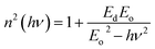
The Wemple–DiDomenico single oscillator model was used to study the dispersion behaviour of refractive index which is expressed by the relation,63| |
 | (10) |
where Eo is oscillator energy and Ed is the dispersion energy that measures the average strength of inter band optical transitions. Fig. 9 shows the graph between (n2 − 1)−1 vs. (hν)2 from which the straight-line fitting gives the intercept  and slope (EoEd)−1. The value of Eo and Ed were calculated from the slope and intercept and tabulated in Table 1. The Eo and Ed value increased with annealing temperature as shown in Table 1. Since, Eo is considered as an average of the Eg, our result shows Eo ≈ 2Eg. The increase in Eo shows the increase in inter band transition. Also, it corresponds to the distance between the centre of gravity of the valence and conduction bands. The increase in Ed with annealing temperature is due to the increase of diffusion of atoms to the interstitial sites.64
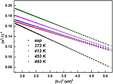 |
| | Fig. 9 (n2 − 1)−1 vs. (hν)2 plot of the studied films. | |
The oscillator strength of the films is given by the relation65
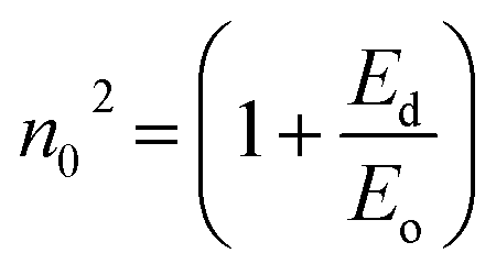
The values of oscillator strength are presented in Table 1 which indicates the increase of strength with annealing. The static refractive index of all the studied films was obtained by using the equation
| |
 | (12) |
The obtained values of n0 are listed in Table 2.
Table 2 Optical parameters of the studied films
| Sample |
ε∞ |
N/m* × 1056 (m−3 kg−1) |
n0 |
χ(3) (×10−11 esu) at hν = 2.03 eV |
n2 (×10−10 esu) at hν = 2.03 eV |
| As-prepared |
5.123 |
3.552 |
2.22 |
5.38 |
9.2 |
| 373 K |
5.472 |
2.861 |
2.26 |
2.47 |
4.18 |
| 413 K |
5.621 |
1.925 |
2.39 |
2.34 |
3.66 |
| 453 K |
5.813 |
1.685 |
2.40 |
2.08 |
3.24 |
| 493 K |
5.921 |
1.014 |
2.41 |
1.63 |
2.51 |
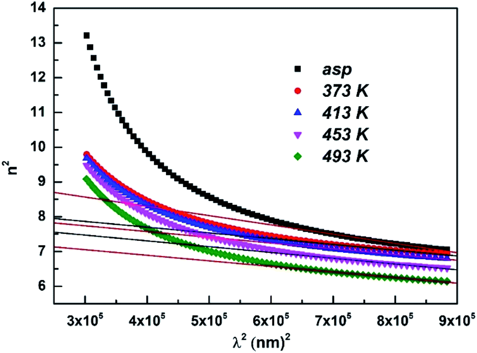
3.10. High frequency dielectric constant and carrier concentration
The calculated values of refractive index were used to find the high frequency dielectric constant (ε∞) and carrier concentration (N/m*) according to the relation9| |
 | (13) |
where ε1 the real part of the dielectric constant, e is charge of electron, N is the free charge carrier concentration, ε0 is the permittivity of free space, m* is the effective mass of charge carrier and c is the velocity of light. The graph between n2 vs. λ2 is shown in Fig. 10 in which the linear fitting gives the value of ε∞ as intercept and the slope gives the value of N/m*. The calculated values of ε∞ and N/m* for the as-prepared and annealed films are presented in Table 2. It shows that the ε∞ values increased whereas the carrier concentration decreased.
 |
| | Fig. 10 n2 vs. λ2 plot of the studied films. | |
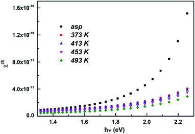
3.11. Nonlinear optical properties
3rd order nonlinear susceptibility (χ(3)). The nonlinear effects play a significant role in chalcogenide films as the response of the material depends nonlinearly on the strength of the electric field. The origin of the optical nonlinearity in chalcogenide materials is due to the nuclear interactions with αp and its effect on bond lengths. The importance of χ(3) lies on its dependence on linear refractive index which in turn applied to the frequency conversion and optical switching devices.66Ticha and Tichy67 combined the Miller's rule68 with that of the Wemple–DiDomenico single effective oscillator model for the estimation of χ(3) since Ed and Eo are related to the chemistry of a material.
According to Miller, the relation between the linear susceptibility χ(1) and nonlinear susceptibility χ(3) is given by
where
A = 1.7 × 10
−10 (
χ measured in esu).
The linear optical susceptibility for chalcogenide glasses in the first approximation is given by the relation
By using eqn (15) in eqn (14) we can write
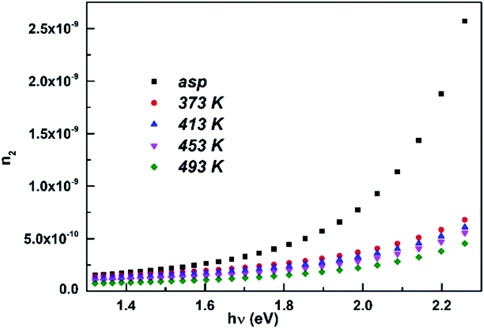
The obtained values of χ(3) vs. hν is plotted in Fig. 11 which shows the decrease of χ(3) with annealing temperature and increase with photon energy. The value of χ(3) at 2.03 eV is presented in Table 2.
 |
| | Fig. 11 χ(3) vs. hν at various annealing temperatures. | |
It is noticed that the value of χ(3) decreased with increase in annealing temperature that infers the changes in material structure. The reason is that annealing process increases the homogenization and polymerization due to increasing rates of chemical reactions among the fragments. The lone pair orbitals present in chalcogenides can be easily polarized which generally play an important role in nonlinear effects in chalcogenide glasses.
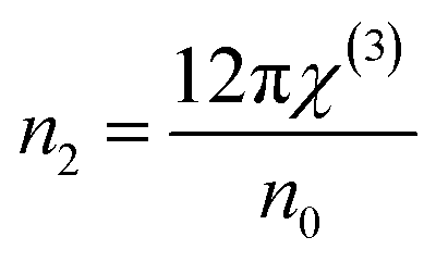
3.12. Nonlinear refractive index (n2)
The nonlinear refractive index (n2) is related to the third-order susceptibility χ(3) and static refractive index (n0) by the Miller's generalized relation which is given by| |
 | (17) |
The variation of n2 with photon energy is shown in Fig. 12 and its value at 2.03 eV is presented in Table 2. The n2 value decreased with annealing temperature like decrease in linear refractive index. Due to the decrease in homo-polar bonds, the probability of variety of defects in gap states decreased and this leads to the decrease in nonlinearity upon annealing. The reduction of n2 and χ(3) upon annealing is useful for solid state laser and UV nonlinear materials.69
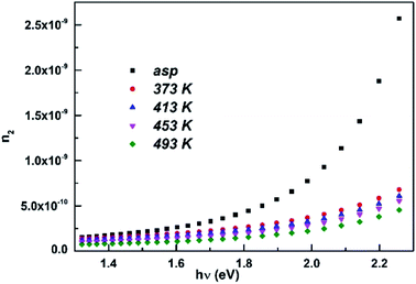 |
| | Fig. 12 Variation of n2 with hν at various annealing temperature. | |
3.13. X-ray diffraction study
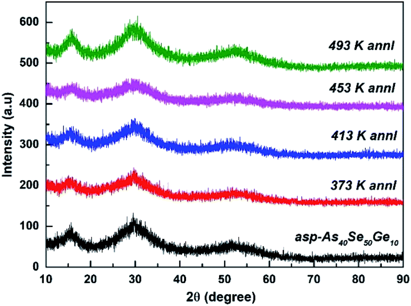
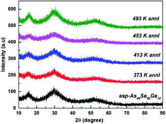
Fig. 13 represents the X-ray diffraction patterns of as-prepared and annealed As40Se50Ge10 films at 373, 413, 453 and 493 K. There exists one broad hump between 20–35° and small hump between 10–20° which confirms the amorphous structure of the films. The annealing induces no structural change as cleared from XRD pattern.
 |
| | Fig. 13 XRD patterns of as-prepared and annealed As40Se50Ge10 thin films. | |
3.14. EDAX and SEM analysis
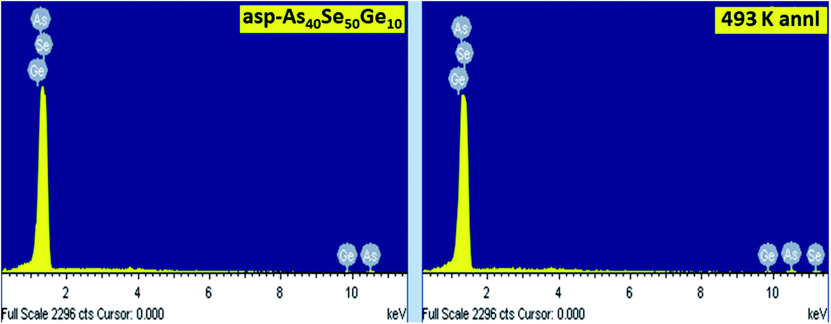
The presence of As, Se and Ge in both as-prepared and annealed films were checked by EDAX as shown in Fig. 14. The different peaks correspond to the respective elements and composition of different films is nearly same and within 3% error from the calculated value.
 |
| | Fig. 14 EDAX picture of as-prepared and 493 K annealed thin film. | |
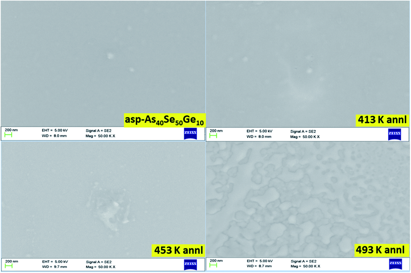
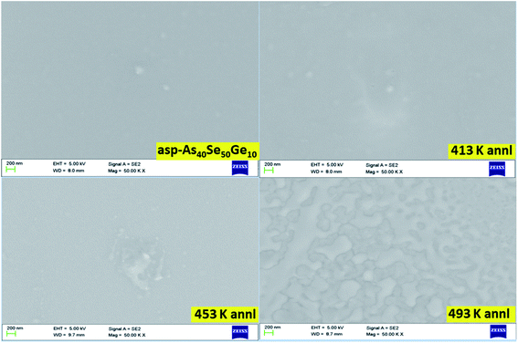
The FESEM pictures of as-prepared and annealed As40Se50Ge10 films are shown in Fig. 15. It is clear from the figures that the films are homogeneous and smooth as we have taken precautions to form homogeneous and uniform film by constant rotation of the substrate while preparing the film. The differences in the images can be visible due to the annealing process. However, there is not much change in the structure except the film at 493 K which shows fragmentation.
 |
| | Fig. 15 FESEM picture of as-prepared and annealed thin films. | |
3.15. Raman analysis
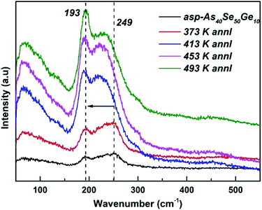
The Raman spectroscopy gives required structural information of the material in terms of chemical bond and atomic arrangement. The Raman spectra for the as-prepared and annealed films are shown in Fig. 16 in which the as-prepared film contains peaks at 193 cm−1, 230 cm−1 and 249 cm−1. The peak at 193 cm−1 corresponds to A1 mode, which is ν1 symmetric stretching vibration mode of Ge–Se bonds in GeSe4/2 corner-sharing tetrahedral unit.70 It can be seen that with annealing, the intensity of this peak increased which shows the increase of Ge–Se heteropolar bonds as suggested in eqn (5). The broad main vibrational band at 230 cm−1 is assigned to the As–Se vibration of symmetric stretching of pyramidal structural units of AsSe3/2.71 This peak is also found to be more intense than the as-prepared one upon annealing which infers the increase of As–Se bonds. The peak at 249 cm−1 corresponds to the Se–Se bonds in Se8 ring like or chain like structures.72 This peak is found to be diminished with annealing which shows the reduction in Se–Se homopolar bonds. The change in intensity and peak shifting in these films clearly shows the annealing effect.
 |
| | Fig. 16 Raman spectra of as-prepared and annealed thin film. | |
4. Conclusion
The study reports the thermal annealing effect on the optical parameters of the films. The transition in these films is indirect allowed type and the band gap increased with annealing is due to the decrease in density of defect states in the localized region. The decrease in disorder with annealing resulted the increase in band gap. The dispersion and nonlinear parameters are found to be sensitive to the annealing temperature. The linear refractive index and extinction coefficient decreased while Eo and Ed values increased thus increasing the oscillator strength. The ε∞ values increased whereas the carrier concentration decreased. The χ(3) and n2 decreased with annealing that is useful for solid state laser and UV nonlinear materials. The decrease in optical conductivity with annealing is due to the reduction in defect states. The dielectric loss factor decreased with annealing. No structural change was found from the XRD study while the Raman shift confirmed the homopolar to heteropolar bond transformation.
Conflicts of interest
There are no conflicts of interest for this manuscript.
References
- B. J. Eggleton, B. Luther-Davies and K. Richardson, Chalcogenide photonics, Nat. Photonics, 2011, 5, 141–148 CrossRef CAS
 .
. - C. Quémard, F. Smektala, V. Couderc, A. Barthelemy and J. Lucas, Chalcogenide glasses with high non-linear optical properties for telecommunications, J. Phys. Chem. Solids, 2001, 62(8), 1435–1440 CrossRef .
- A. Zakery and S. R. Elliott, Optical properties and applications of chalcogenide glasses: a review, J. Non-Cryst. Solids, 2003, 330, 1–12 CrossRef CAS .
- A. Seddon, Chalcogenide glasses, a review of their preparation, properties and applications, J. Non-Cryst. Solids, 1995, 184, 44–50 CrossRef CAS .
- M. Frumar, J. Jedelský, B. Frumarová, T. Wágner and M. Hrdlička, Optically and thermally induced changes of structure, linear and non-linear optical properties of chalcogenides thin films, J. Non-Cryst. Solids, 2003, 326–327, 399–404 CrossRef .
- R. Naik, C. Sripan and R. Ganesan, Photodarkening in As50Se50 thin films by 532 nm laser irradiation, Opt. Laser Technol., 2017, 90, 158–164 CrossRef CAS .
- A. A. El-Sebaii, S. A. Khan, F. M. Al-Marzouki, A. S. Faidah and A. A. Al-Ghamdi, Role of heat treatment on structural and optical properties of thermally evaporated Ga10Se81Pb9 chalcogenide thin films, J. Lumin., 2012, 132(8), 2082–2087 CrossRef CAS .
- M. Behera, R. Naik, C. Sripan, R. Ganesan and N. C. Mishra, Influence of Bi content on linear and nonlinear optical properties of As40Se60−xBix chalcogenide thin films, Curr. Appl. Phys., 2019, 19(8), 884–893 CrossRef .
- H. E. Atyia and N. A. Hegab, Influence of thermal treatment on the optical aspects for Ge20In5Se75 films, Optik, 2016, 127, 3888–3894 CrossRef CAS .
- R. Panda, M. Panda, H. Rath, B. N. Dash, K. Asokan, U. P. Singh, R. Naik and N. C. Mishra, Structural and morphological modifications of AgInSe2 and Ag2Se composite thin films on 140 MeV Ni ion irradiation, Appl. Surf. Sci., 2019, 479, 997–1005 CrossRef CAS .
- R. P. Wang, S. J. Madden, C. J. Zha and A. V. Rode, Annealing induced phase transformations in amorphous As2S3 films, J. Appl. Phys., 2006, 100, 063524 CrossRef .
- N. Teng, J. Qina, Y. Chena, R. Wang, X. Shen and T. Xu, Optical properties and thermal stability of amorphous Ge–Sb–Se films, J. Non-Cryst. Solids, 2020, 532, 119888 CrossRef CAS .
- R. Ya. Golovchaka, S. A. Kozyukhinb, A. Kozdrasc, O. I. Shpotyuka and V. M. Novotortsev, Physical aging of chalcogenide glasses, Inorg. Mater., 2010, 46, 911–913 CrossRef .
- M. Caravacaa and J. Abad, Evidence of aging in glassy chalcogenides: numerical simulations in the electron glass model, Chalcogenide Lett., 2014, 11, 287–295 Search PubMed .
- F. Lin and P. Lucas, Competition between photo relaxation and photoexcitation in chalcogenide glasses and the effect of aging, J. Non-Cryst. Solids, 2011, 357, 888–892 CrossRef CAS .
- O. I. Shpotyuk and R. Y. Golovchak, Physical aging effects in selenide glasses accelerated by highly energetic γ-irradiation, J. Non-Cryst. Solids, 2006, 352, 704–708 CrossRef CAS .
- R. C. Welch, J. R. Smith, M. Potuzak, X. Guo, B. F. Bowden, T. Kiczenski, D. C. Allan, E. A. King, A. J. Ellison and J. C. Mauro, Dynamics of glass relaxation at room temperature, Phys. Rev. Lett., 2013, 110(26), 265901 CrossRef PubMed .
- R. D. Priestley, Physical aging of confined glasses, Soft Matter, 2009, 5(5), 919–926 RSC .
- S. Geiger, Q. Du, B. Huang, M. Y. Shalaginov, J. Michon, H. Lin, T. Gu, A. Yadav, K. A. Richardson, X. Jia and J. Hu, Understanding aging in chalcogenide glass thin films using precision resonant cavity refractometry, Opt. Mater. Express, 2019, 9, 2252 CrossRef CAS .
- J. S. Sanghera and I. D. Aggarwal, Active and passive chalcogenide glass optical fibers for IR applications: a review, J. Non-Cryst. Solids, 1999, 256&257, 6–16 Search PubMed .
- A. Feltz, Amorphous and Vitreous Inorganic Solids, Mir, Moscow, 1986 Search PubMed .
- P. Boolchand, G. Lucovsky, J. C. Phillips and M. F. Thorpe, Self-organization and the physics of glassy networks, Phil. Mag., 2005, 85, 3823–3838 CrossRef CAS .
- A. B. Seddon and M. J. Laine, Chalcogenide glasses for acousto-optic devices. II. As–Ge–Se systems, J. Non-Cryst. Solids, 1997, 213 & 214, 168–173 Search PubMed .
- J. Cheng, G. Tilloca and J. Zarzycki, Infra-red transmitting glass-ceramics of the As-Ge- Se system nucleated by zirconium selenide, J. Mater. Sci., 1981, 16, 2531–2543 CrossRef CAS .
- B. Zhang, W. Guo, Y. Yu, Ch. Zhai, S. Qi, A. Yang, L. Li, Zh. Yang, R. Wang, D. Tang, G. Tao and B. Luther-Davies, Low Loss, High NA chalcogenide glass fibers for broadband mid-infrared supercontinuum generation, J. Am. Ceram. Soc., 2015, 98, 1389–1392 CrossRef CAS .
- D. A. P. Bulla, R. P. Wang, A. Prasad, A. V. Rode, S. J. Madden and B. Luther-Davies, On the properties and stability of thermally evaporated Ge-As-Se thin films, Appl. Phys. A: Mater. Sci. Process., 2009, 96, 615–625 CrossRef CAS .
- P. Hawlova, M. Olivier, F. Verger, V. Nazabal and P. Nemec, Photosensitivity of pulsed laser deposited Ge20As20Se60 and Ge10As30Se60 amorphous thin films, Mater. Res. Bull., 2013, 48(10), 3860–3864 CrossRef CAS .
- Z. Zhang, S. Xu, Y. Chen, X. Shen and R. Wang, Photo-induced effects in Ge–As–Se films in various states, Opt. Mater. Express, 2020, 10, 540–548 CrossRef .
- J. T. Gopinath, M. Sojacic, E. P. Ippen, V. N. Fuflyingin, W. A. King and M. Shurgailn, J. Appl. Phys., 2004, 96, 6931 CrossRef CAS .
- R. Chauhan, A. Tripathi, A. K. Srivastava and K. K. Srivastava, Effect of swift heavy ion irradiation on optical and structural properties of amorphous Ge–As–Se thin films, Chalcogenide Lett., 2013, 10, 63–71 CAS .
- A. M. Andriesh, Chalcogenide glasses in optoelectronics, Fiz. Tekh. Poluprovodn., 1998, 32, 970–975 CAS .
- E. R. Skordeva and D. D. Arsova, A topological phase transition in ternary chalcogenide films, J. Non-Cryst. Solids, 1995, 192&193, 665–668 Search PubMed .
- R. Naik, J. Pradhan, C. Sripan and R. Ganesan, Influence of Ge addition on the optical properties of As40Se50Ge10 thin film probed by spectroscopy techniques, Phase Transitions, 2018, 91, 477–489 CrossRef CAS .
- Z. Tang, V. S. Shiryaev, D. Furniss, L. Sojka, S. Sujecki, T. M. Benson, A. B. Seddon and M. F. Churbanov, Low loss Ge–As–Se chalcogenide glass fiber, fabricated using extruded preform, for midinfrared photonics, Opt. Mater. Express, 2015, 5, 1722–1737 CrossRef CAS .
- A. M. Adam, E. Lilov, V. Lilova and P. Petkov, Characterization and optical properties of bismuth chalcogenide films prepared by pulsed laser deposition technique, Mater. Sci. Semicond. Process., 2017, 57, 210–219 CrossRef CAS .
- M. Behera, N. C. Mishra and R. Naik, Thermal annealing induced evolution of Bi3Se2 topological phase from Bi/As2Se3thin film: Structural, optical and morphological study, Phys.
B, 2019, 560, 51–59 CrossRef CAS .
- E. R. Shaaban, Y. A. M. Ismail and H. S. Hassan, Compositional dependence of the optical properties of amorphous Se80−xTe20Bix thin films using transmittance and reflectance measurements, J. Non-Cryst. Solids, 2013, 376, 61–67 CrossRef CAS .
- R. Naik, P. P. Sahoo and C. Sripan, Laser induced Bi diffusion in As40S60 thin films and the optical properties change probed by FTIR and XPS, Opt. Mater., 2016, 62, 211–218 CrossRef CAS .
- P. Pradhan, R. Naik, N. Das and A. K. Panda, Bandgap tuning in As40Se53Sb07 thin films by 532 nm laser irradiation: an optical investigation by spectroscopic techniques, Opt. Mater., 2017, 75, 699–709 CrossRef .
- A. Aparimita, R. Naik, S. Sahoo, C. Sripan and R. Ganesan, Influence of low energy Ag ion irradiation for formation of Bi2Se3 phase from Bi/GeSe2 heterostructure thin films, Appl. Phys. A, 2020, 126, 203 CrossRef CAS .
- A. M. Abdelraheem, M. I. Abd-Elrahman, M. Mohamed, N. M. A. Hadia and E. R. Shaaban, Linear and non-linear optical parameters of diluted magnetic semiconductor CdS0.9Mn0.1 thin film: Influence of the film thickness, J. Electron. Mater., 2020, 49, 1944–1956 CrossRef CAS .
- A. Aparimita, R. Naik, C. Sripan and R. Ganesan, Laser-induced optical photobleaching in Bi-doped Ge30Se70 amorphous thin films, Appl. Phys. A, 2020, 126, 5 CrossRef CAS .
- H. Hosni, S. Fayek, S. El-Sayed, M. Roushdy and M. Soliman, Optical properties and DC electrical conductivity of Ge28−xSe72Sbx thin films, Vacuum, 2006, 81, 54–58 CrossRef CAS .
- R. Naik, A. Aparimita, D. Alagarasan, S. Varadharajaperumal and R. Ganesan, Linear and nonlinear optical properties change in Ag/G heterostructure thin films by thermal annealing and laser irradiation, Opt. Quantum Electron., 2020, 52, 136 CrossRef CAS .
- J. Tauc, Amorphous and liquid semiconductors, Plenum Press, New York, 1974, p. 171 Search PubMed .
- A. S. Hassanien and I. Sharma, Band-gap engineering, conduction and valence band positions of thermally evaporated amorphous Ge15-xSbxSe50Te35 thin films: Influences of Sb upon some optical characterizations and physical parameters, J. Alloys Compd., 2019, 798, 750–763 CrossRef CAS .
- M. Behera and R. Naik, Optical properties change in laser-induced Te/As2Se3 chalcogenide thin films, Appl. Phys. A, 2016, 122, 913–919 CrossRef .
- N. F. Mott, E. A. Davis, Electronics Processes in Non-crystalline Materials, Clarendon, Oxford ( 1979) p. 428 Search PubMed .
- M. M. El-Nahass, M. H. Ali and I. T. Zedan, Photo induced changes in linear and nonlinear optical properties of Ge10In10Se80 thin films, J. Non-Cryst. Solids, 2014, 404, 78–83 CrossRef CAS .
- R. Panda, R. Naik and N. C. Mishra, Thermal annealing induced evolution of AgIn5Se8 phase from Ag/In2Se3 bilayer thin film, J. Alloys Compd., 2019, 778, 819–826 CrossRef CAS .
- A. R. Zanatta and I. Chambouleyron, Absorption edge, band tails and disorder of amorphous semiconductors, Phys. Rev. B: Condens. Matter Mater. Phys., 1996, 53, 3833–3836 CrossRef CAS PubMed .
- F. Urbach, The long-wavelength edge of photographic sensitivity and of the electronic absorption of solids, Phys. Rev., 1953, 92, 1324 CrossRef CAS .
- J. Olley, Structural disorder and Urbach rule, Solid State Commun., 1973, 13, 1437–1440 CrossRef CAS .
- P. Pradhan, R. Naik, N. Das and A. K. Panda, Laser induced optical properties change by photo diffusion of Sb into As2Se3 chalcogenide thin films, Opt. Laser Technol., 2017, 96, 158–165 CrossRef CAS .
- N. M. Kamble, R. B. Tokas, A. Biswas, S. Thakur, D. Bhattacharya and N. K. Sahoo, Determination of the optical constants of HfO2–SiO2 composite thin films through reverse fitting of transmission spectra, Vacuum, 2011, 86, 422 CrossRef CAS .
- S. Jena, R. B. Tokas, N. Kamble, S. Thakur, D. Bhattacharyya and N. K. Sahoo, Investigation of elastic and optical properties of electron beam evaporated ZrO2–MgO composite thin films, Thin Solid Films, 2013, 537, 163–170 CrossRef CAS .
- A. A. Attia, M. M. El-Nahass, M. Y. El-Bakry and D. M. Habashy, Neural networks modelling for refractive indices of semiconductors, Opt. Commun., 2013, 287, 140–144 CrossRef CAS .
- R. Naik, S. Jena, R. Ganesan and N. K. Sahoo, Effect of laser irradiation on optical properties of Ge12Sb25Se63 amorphous chalcogenide thin films, Indian J. Phys., 2015, 89, 1031–1040 CrossRef CAS .
- M. M. El-Nahass, H. S. Soliman, B. A. Khalifa and I. M. Soliman, Structural and optical properties of nanocrystalline aluminum phthalocyanine chloride thin films, Mater. Sci. Semicond. Process., 2015, 38, 177–183 CrossRef CAS .
- F. Yakuphanoglu, A. Cukurovali and I. Yilmaz, Refractive index and optical absorption properties of the complexes of a cyclobutane containing thiazolyl hydrazone ligand, Opt. Mater., 2005, 27, 1363 CrossRef CAS .
- N. A. Bakr, A. Funde, V. Waman, M. Kamble, R. Hawaldar, D. Amalnerkar, S. Gosavi and S. Jadkar, Determination of the optical parameters of a-Si:H thin films deposited by hot wire–chemical vapour deposition technique using transmission spectrum only, Pramana, 2011, 76, 519 CrossRef CAS .
- K. R. Rajesh and C. S. Menon, Estimation of the refractive index and dielectric constants of magnesium phthalocyanine thin films from its optical studies, Mater. Lett., 2002, 53, 329–332 CrossRef CAS .
- S. H. Wemple and M. DiDomenico, Behavior of the electronic dielectric constant in covalent and ionic materials, Phys. Rev. B: Solid State, 1971, 3, 1338 CrossRef .
- V. D. Das and R. C. Mallik, Study of scattering of charge carriers in thin films of (Bi0.25Sb0.75)2Te3 alloy with 2% excess Te, Mater. Res. Bull., 2002, 37, 1961–1971 CrossRef CAS .
- M. M. El-Nahass, M. M. Sallam, M. A. Afifi and I. T. Zedan, Structural and optical properties of polycrystalline CdSexTe1−x (0 ≤ x ≤ 0.4) thin films, Mater. Res. Bull., 2007, 42, 371–384 CrossRef CAS .
- I. Sharma, S. K. Tripathi and P. B. Barman, Thickness-dependent optical properties and nonlinear refractive index of a-Ge-Se-In thin films, Phase Transitions, 2014, 87, 363–375 CrossRef CAS .
- H. Ticha and L. Tichy, Semiempirical relation between non-linear susceptibility (refractive index), linear refractive index and optical gap and its application to amorphous chalcogenides, J. Optoelectron. Adv. Mater., 2002, 4(2), 381–386 CAS .
- J. J. Wynne, Optical third-order mixing in GaAs, Ge, Si, and InAs, Phys. Rev., 1969, 178(3), 1295 CrossRef CAS .
- X. Dong, L. Huang, Q. Liu, H. Zeng, Z. Lin, D. Xu and G. Zou, Perfect balance harmony in Ba2NO3(OH)3:a beryllium-free nitrate as a UV nonlinear optical material, Chem. Commun., 2018, 54, 5792–5795 RSC .
- P. Němec, B. Frumarova and M. Frumar, Structure and properties of the pure and Pr3+-doped Ge25Ga5Se70 and Ge30Ga5Se65 glasses, J. Non-Cryst. Solids, 2000, 270, 137–146 CrossRef .
- V. S. Vassilev, Z. G. Ivanova, L. Aljihmani, E. Cernoskova and Z. Cernosek, Glass-forming regions, properties, and structure of the chalcogenide As2Se3–GeSe2–SnTe (Ag4SSe) systems, Mater. Lett., 2005, 59, 85–87 CrossRef CAS .
- Y. Chen, X. Shen and R. Wang, et al., Optical and structural properties of Ge–Sb–Se thin films fabricated by sputtering and thermal evaporation, J. Alloys Compd., 92013, 548, 155–160 CrossRef .
|
| This journal is © The Royal Society of Chemistry 2020 |
Click here to see how this site uses Cookies. View our privacy policy here. 
 Open Access Article
 This Open Access Article is licensed under a Creative Commons Attribution-Non Commercial 3.0 Unported Licence
 *a
*a


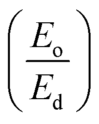 and slope (EoEd)−1. The value of Eo and Ed were calculated from the slope and intercept and tabulated in Table 1. The Eo and Ed value increased with annealing temperature as shown in Table 1. Since, Eo is considered as an average of the Eg, our result shows Eo ≈ 2Eg. The increase in Eo shows the increase in inter band transition. Also, it corresponds to the distance between the centre of gravity of the valence and conduction bands. The increase in Ed with annealing temperature is due to the increase of diffusion of atoms to the interstitial sites.64