
 Open Access Article
 This Open Access Article is licensed under a
 Creative Commons Attribution 3.0 Unported Licence
Symmetric accelerating beam generation via all-dielectric metasurfaces
Hammad Ahmed *a,
Arbab Abdur Rahim*a,
Muhammad Mahmood Alib and
Husnul Maaba
*a,
Arbab Abdur Rahim*a,
Muhammad Mahmood Alib and
Husnul Maaba
aGhulam Ishaq Khan Institute of Engineering Sciences and Technology, Swabi, 23460, Pakistan. E-mail: arbab@giki.edu.pk; hammmaad.ahmed@gmail.com
bOptical Fibre Sensors Research Centre, Department of Electronics and Computer Engineering, University of Limerick, Limerick, V94 T9PX, Ireland
First published on 17th August 2020
Abstract
Traditionally, symmetric accelerating beam (SAB) generation requires bulky optical components, which hinder the miniaturization of optical systems. Recently, metasurfaces, which are composed of sub-wavelength features, have provided a captivating boulevard for the realization of ultra-thin and flat optical devices. Therefore, for the first time, we design and simulate all-dielectric metasurfaces based on an optical caustic approach to generate highly efficient SABs by tailoring the phase of an incident wave. The designed metasurface utilizes spatial distribution of optimized Nb2O5 nano-rods on SiO2 substrate to perform the phase modulation. In contrast with conventional accelerating beams, the generated SABs can follow any predefined propagation trajectory with unique features, such as symmetric intensity profile, autofocusing, and thin needle-like structure in their intensity profile. In addition to this, these beams have also shown the ability to avoid obstacles, placed in the direction of propagation of main lobes. We believe that these beams can be useful in applications, including Raman spectroscopy and fluorescent imaging, and multiparticle manipulation.
Introduction
Over the past few years, accelerating beams have attracted the attention of researchers owing to their unprecedented properties, i.e., non-diffraction, self-acceleration, and self-healing. Inspired by Berry and Balazs' work,1 these beams were first experimentally demonstrated in 2007.2 Since then, self-accelerating beams are considered as an important area of research in the field of optical beams and particle manipulation. The conventional method to generate these beams includes a spatial light modulator (SLM) to impart the desired phase mask on an incident beam.3 However, this method usually required a Fourier Transform (FT) lens which makes the optical system bulky and thus, difficult to incorporate in photonic integrated circuits (PICs).4 Moreover, the larger pixel size of SLM affects the performance of optical systems.5Metasurfaces, two-dimensional metamaterials provide a remarkable platform to replace the conventional accelerating beam generators. Metasurfaces have intriguing capabilities to mould the incident light to any desired form. By the virtue of subwavelength nano-resonators (unit cells), metasurfaces can tailor the polarization, phase, and amplitude of impinging light to generate high-quality accelerating beam and overcome the limitations imposed by the SLM. Furthermore, several exotic phenomena have been realized through metasurfaces, such as hologram,6,7 meta-lens,8,9 optical vortex,10 meta-polarizer,11–13 sensing,14 and beam splitter.11,15 Recently, numerous metasurfaces have been proposed to demonstrate the accelerating beam generation. Li et al.,4 Song et al.,16 Xu et al.,17 and Wang et al.18 have utilized the approach of simultaneous phase and amplitude modulation to generate the accelerating beams via plasmonic transmission-type metasurfaces. Subsequently, in another approach, Wang et al.,19 has employed the cubic phase on dielectric metasurfaces and generated the accelerating beam at the back focal plane. However, it is worth mentioning here that most of these beams typically follow a fixed parabolic trajectory, which limits its robustness for practical applications. Therefore, to outclass this drawback, Ahmed et al.,20 Guo et al.,21 and Fan et al.5 have utilized the optical caustic approach to realize the accelerating beams, which can propagate along arbitrary directions. Since then, the control of propagation trajectory has become increasingly interesting area of research.
Inspired from the previous work, herein, we propose single-layered, ultra-thin, all-dielectric metasurfaces for symmetric accelerating beam (SAB) generation. This idea was first theoretically presented in ref. 22. Later on, in 2014 and 2019, the SABs were realized for the first time by utilizing SLM.23,24 As discussed earlier, to overcome limitations of SLM, metasurfaces are the best choice. Here, phase profiles of SABs are derived using the optical caustic approach. Then, the derived phase profiles are spatially distributed on metasurface through niobium pentoxide (Nb2O5) nano-rods. The Nb2O5 is chosen because it has low absorption at 355 nm (UV domain) compared to other state-of-the-art materials such as titanium oxide (TiO2), silicon nitride (Si3N4), amorphous silicon hydrogenated (a-Si:H) and gallium nitride (GaN).25,26 This unique property of low absorption is responsible for high transmission efficiency.27 In this work, the phase manipulation of an incident linearly polarized light is performed by varying radii of well-optimized nano-rods while maintaining the high transmission efficiency. Nano-rod geometry is adopted to achieve the polarization-insensitive feature.28 This approach is effective in a way that it can alleviate challenges of conventional SLM base SAB generator and can straightforwardly be downsized for on-chip applications. Moreover, symmetric intensity pattern of SAB can manipulate the multiple particles. This property can circumvent requirement of alignment system between the beam and particles.22 Thus, simplifying experimental setup for trapping the micro-particles. Besides, SABs also contain a needle-like structure in its intensity profile, which can be used in fluorescent imaging and Raman spectroscopy.29,30 Furthermore, we also show the autofocusing characteristic of SABs, which can be used in laser ablation and nano-surgery.24
Design methodology
To design all-dielectric metasurfaces, nano-resonators with varying geometric parameter are spatially distributed at the interface to achieve full control over an incident wave. In this regard, we chose the nano-rod of Nb2O5 with a fixed height on SiO2 (glass) substrate whose schematic diagram is illustrated in Fig. 1(a). Here, R is the radius of nano-rod, P represents the periodicity, and H is the height. The realization of any phase-sensitive optical phenomenon via metasurfaces necessitates that each nano-rod should impart a defined phase to substantiate the desire optical response. Therefore, we optimize our nano-rod in such a way to attain the complete 2π phase coverage while maintaining the maximum possible transmission efficiency (85%). Here, the nano-rod act as a truncated waveguide which works on the wave-guiding effect.31 This effect can be better explained through the following relation:32
 | (1) |
 | ||
| Fig. 1 Unit cell design. (a) Schematic depiction of Nb2O5 nano-rod on SiO2 substrate. (b) neff of propagation mode as a function of radius. Insets show the confinement of propagation mode inside the nano-cylinder at some selected radii (R = 30, 50, 70 and 90 nm). The cylindrical grid indicates the boundary of a Nb2O5 nano-rod. (c) Transmission efficiency map. The white dashed line sketched on the map (at P = 182 nm with R ranging from 30 nm to 100 nm) where the average transmission efficiency is greater than 85%. (d) Complete 2π phase coverage and control over the wave-front is achieved by an array of eight nano-rods of different radii with the fixed height of 430 nm. | ||
To confirm complete phase modulation, the numerical optimization of the unit cell is performed through the Finite-Difference-Time-Domain (FDTD) solver. The unit cell is simulated with Perfectly-Matched-Layered (PML) boundary conditions in z-axis while periodic boundaries in x- and y-axis. The x-polarized light is impinged from the backside of the unit cell. The optimization results reveal that P of 182 nm, H of 430 nm and range of R from 30 nm to 90 nm can acquire the complete (0–2π) phase coverage (as shown in Fig. 1(d) along with high transmission efficiency (Fig. 1(c))).
Fig. 2 shows the working principle of our accelerating beam generating metasurfaces where nano-rods of 430 nm height are spatially distributed on a SiO2 substrate. The metasurfaces is illuminated with an x-polarized plane wave to generate the desired self-accelerating beam. The main aim is to encode a metasurface with a suitable phase profile ϕ(x), that can generate a self-accelerating beam with predefined propagation trajectory x = f(z). Fig. 2(a) elucidates the schematic diagram of our model. It demonstrates that an accelerating beam can be treated as an optical caustic, that can be described by the family of rays (tangent to the caustic surface) emanating from the metasurfaces, which eventually converges to a focal line x = f(z). Each point on metasurfaces can be functionally related to the corresponding point on optical caustic through the tangent of a slope. Therefore, the slope of optical caustic at an arbitrary point C can be defined as 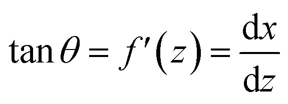 . Whereas, the desired phase that can be spatially distributed along metasurfaces is given as:34
 | (2) |
 is the wavenumber and λ is the operating wavelength. Eqn (2) can be further simplified by assuming paraxial approximation, because, in current form, it is difficult to solve this integration analytically. Consequently, the simplified case can be given as:
 | (3) |
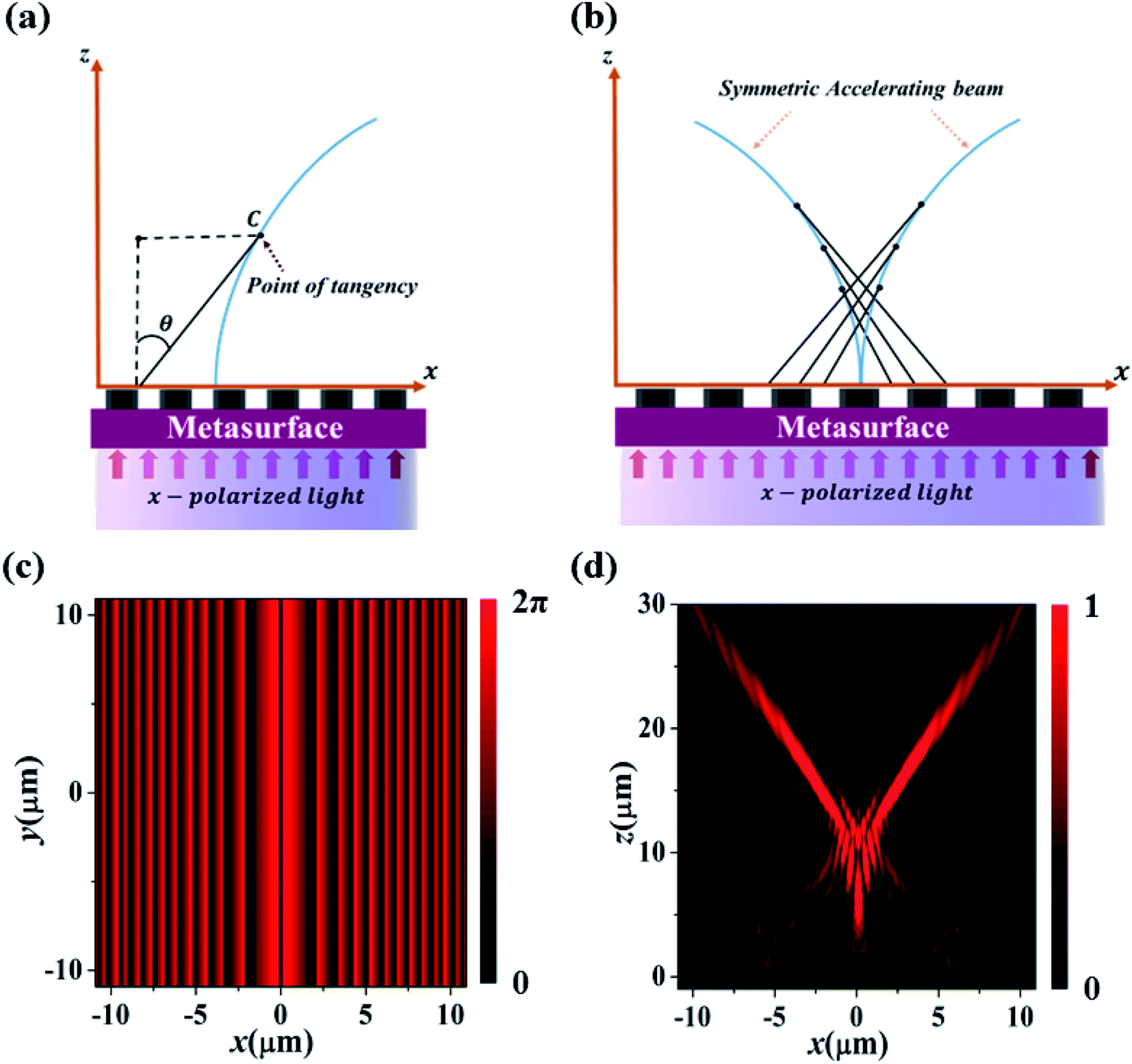 | ||
| Fig. 2 Proposed model based on an optical caustic approach. (a) Asymmetric self-accelerating beam generation. (b) Symmetric self-accelerating beam generation. (c and d) SAB generation with parabolic propagation. (c) Calculated phase profile. (d) Simulated electric field distribution in x–z plane. | ||
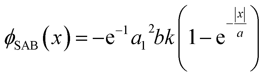
To design a metasurface capable of generating SAB, herein, the mirror-symmetry of phase ϕ(x) is performed, i.e., ϕSAB(x) = ϕ(|x|). The ϕSAB(x) corresponds to the symmetric phase profile. The phase profile ϕSAB(x) shows a perfect symmetry about the optical axis because ϕSAB(x) = ϕSAB(−x) is an even function.24 Therefore, when metasurface is encoded with ϕSAB(x), a SAB will be generated as shown in conceptual Fig. 2(b). In contrast to conventional accelerating beam, SAB possesses a symmetric intensity profile which is composed of two separate accelerating beams, that can manipulate multiple particle. Therefore, such highly structured beams can simplify the experimental setup for optical tweezers, as the symmetric intensity pattern overcomes the requirement of alignment system between the beam and particle.22,24,35
Numerical results and discussion
First, we consider the SABs propagating along the parabolic path (x = ±az2). Then, from eqn (3), the corresponding phase distribution for parabolic propagation is calculated, which can be expressed as:
 | (4) |
 | ||
| Fig. 3 Normalized intensity profiles recorded at (a) z = 7.5 μm, (b) 15 μm, and (c) 18 μm. Simulated electric field distributions of thin needle like structure SABs for (d) a = 0.012 (e) a = 0.009 and (f) a = 0.006. | ||
Additionally, a needle-like structure can be observed in electric field intensity distribution, which is formed by the intensity profile of central lobe. The coefficient of acceleration ‘a’ is the key parameter in eqn (4) for controlling the length of the needle. Fig. 3(d–f) illustrate the thin needle-like structure of SAB for a = 0.006, 0.009, and 0.012, respectively. The larger value of ‘a’ produce a shorter needle and vice versa. This fascinating property can help in several important applications, such as fluorescent imaging and second-harmonic generation.30
Furthermore, we extend this approach to generate autofocusing SAB. To realize this, we have to perform the phase shift. The modified phase equation with phase shift factor can be expressed as:
| ϕSAB(x) = ϕ(|x| + Δx) | (5) |
 | ||
| Fig. 4 Autofocusing SAB. (a) Shifted phase profile. (b) Simulated electric field intensity distribution in x–z plane. The solid white line indicates the normalized intensity profile at focal point (z = 11.3 μm). (c and d) SAB generation with natural logarithmic trajectory. (c) Calculated phase profile. (d) Simulated electric field distribution in x–z plane. | ||
As mentioned previously, SABs are optical caustics, that are formed by the family of rays, tangent to the caustic surface. Therefore, apart from the parabolic trajectory, SABs can follow several other caustic trajectories, mentioning couple can be bi-quadratic and natural logarithmic. For illustration purpose, we design a metasurface embedding the phase distribution of SAB (Fig. 4(c)) propagating along the natural logarithmic trajectory (x = ±a1![[thin space (1/6-em)]](https://www.rsc.org/images/entities/char_2009.gif) ln(bz)). The derived phase equation is given as:
ln(bz)). The derived phase equation is given as:
 | (6) |
In the last, a riveting property of the SAB, which is the self-healing, is demonstrated. This attribute allows it to reform itself on encountering any obstruction during its propagation. To verify this property, a scatterer composed of perfect electric conductors (PEC) (shown as a white rectangular box in Fig. 5) is placed in the path of mains lobes of parabolic and natural logarithmic SABs. The size of the scatterer is kept at P × P × P nm3, where, P = 182 nm. From the simulated electric field distribution presented in Fig. 5(a) and (b), it can be seen that main lobes recover smoothly after passing the scatterer.
 | ||
| Fig. 5 Verification of self-healing property of (a) parabolic and (b) natural logarithmic SABs. White box indicates obstruction, composed of perfect electric conductor (PEC) placed in the path of main lobes. | ||
Conclusions
In summary, we have designed and numerically simulated simple, highly efficient and polarization-insensitive all-dielectric metasurfaces capable of generating highly controllable SABs at 355 nm (UV domain). The proposed design utilizes Nb2O5 nano-rods to manipulate the phase of an impinging wave. The generated non-diffracting and self-healing SABs can propagate along any predefined propagation trajectories. Unlike conventional accelerating beam, SABs possess symmetric intensity pattern, that can manipulate multiple particles simultaneously. Furthermore, the numerical simulation confirms that these beams have a thin needle-like structure in their intensity distribution and demonstrate the autofocusing feature. We anticipate that such captivating features can have potential applications in the field of optical manipulation.Conflicts of interest
The authors declare no conflicts of interest.References
- M. V. Berry and N. L. Balazs, Am. J. Phys., 1979, 47, 264–267 CrossRef.
- G. Siviloglou, J. Broky, A. Dogariu and D. Christodoulides, Phys. Rev. Lett., 2007, 99, 213901 CrossRef CAS PubMed.
- X.-Z. Wang, Q. Li and Q. Wang, Appl. Opt., 2012, 51, 6726–6731 CrossRef PubMed.
- Z. Li, H. Cheng, Z. Liu, S. Chen and J. Tian, Adv. Opt. Mater., 2016, 4, 1230–1235 CrossRef CAS.
- Q. Fan, W. Zhu, Y. Liang, P. Huo, C. Zhang, A. Agrawal, K. Huang, X. Luo, Y. Lu and C. Qiu, Nano Lett., 2018, 19, 1158–1165 CrossRef PubMed.
- M. A. Ansari, T. Tauqeer, M. Zubair and M. Q. Mehmood, Nanophotonics, 2020, 9, 963–971 Search PubMed.
- D. Wen, J. J. Cadusch, J. Meng and K. B. Crozier, Adv. Funct. Mater., 2020, 30, 1906415 CrossRef CAS.
- W. T. Chen, A. Y. Zhu, J. Sisler, Z. Bharwani and F. Capasso, Nat. Commun., 2019, 10, 1–7 CrossRef PubMed.
- T.-Y. Huang, R. R. Grote, S. A. Mann, D. A. Hopper, A. L. Exarhos, G. G. Lopez, G. R. Kaighn, E. C. Garnett and L. C. Bassett, Nat. Commun., 2019, 10, 1–8 CrossRef PubMed.
- H. Ahmed, A. A. Rahim, H. Maab, M. M. Ali, N. Mahmood and S. Naureen, Opt. Mater. Express, 2020, 10, 434–448 CrossRef CAS.
- Z. Guo, L. Zhu, F. Shen, H. Zhou and R. Gao, RSC Adv., 2017, 7, 9872–9879 RSC.
- Y. Chen, J. Gao and X. Yang, Laser Photonics Rev., 2018, 12, 1800198 CrossRef.
- J. Zhou, Y. Wang, M. Lu, J. Ding and L. Zhou, RSC Adv., 2019, 9, 33775–33780 RSC.
- R. Bilal, M. A. Baqir, P. K. Choudhury, M. M. Ali and A. A. Rahim, IEEE Photonics J., 2020, 12, 1–13 Search PubMed.
- H. Ahmed, M. M. Ali, A. Ullah, A. A. Rahim, H. Maab and M. Khan, J. Nanoelectron. Optoelectron., 2019, 14, 1339–1343 CrossRef.
- E. Y. Song, G. Y. Lee, H. Park, K. Lee, J. Kim, J. Hong, H. Kim and B. Lee, Adv. Opt. Mater., 2017, 5, 1601028 CrossRef.
- H. X. Xu, G. Hu, L. Han, M. Jiang, Y. Huang, Y. Li, X. Yang, X. Ling, L. Chen and J. Zhao, Adv. Opt. Mater., 2019, 7, 1801479 CAS.
- T. Wang, G. Zhai, R. Xie, S. Zhu, J. Gao, S. An, B. Zheng, H. Li, Y. Liu and H. Zhang, Adv. Theory Simul., 2019, 2, 1900071 CrossRef.
- H. Wang, J. Du, H. Wang, Y. Lu and P. Wang, Adv. Opt. Mater., 2019, 7, 1900552 CrossRef.
- H. Ahmed, A. A. Rahim, H. Maab, M. M. Ali and S. Naureen, Opt. Mater. Express, 2020, 10, 1083–1091 CrossRef CAS.
- Y. Guo, Y. Huang, X. Li, M. Pu, P. Gao, J. Jin, X. Ma and X. Luo, Adv. Opt. Mater., 2019, 1900503 CrossRef.
- C.-Y. Hwang, D. Choi, K.-Y. Kim and B. Lee, Opt. Express, 2010, 18, 23504–23516 CrossRef PubMed.
- P. Vaveliuk, A. Lencina, J. A. Rodrigo and O. M. Matos, Opt. Lett., 2014, 39, 2370–2373 CrossRef PubMed.
- Y. Qian, H. Mao and S. Lai, Appl. Phys. B: Lasers Opt., 2019, 125, 59 CrossRef.
- Y. Deng, X. Wang, Z. Gong, K. Dong, S. Lou, N. Pégard, K. B. Tom, F. Yang, Z. You and L. Waller, Adv. Mater., 2018, 30, 1802632 CrossRef PubMed.
- K. Huang, J. Deng, H. S. Leong, S. L. K. Yap, R. B. Yang, J. Teng and H. Liu, Laser Photonics Rev., 2019, 13, 1800289 CrossRef.
- N. Mahmood, I. Kim, M. Q. Mehmood, H. Jeong, A. Akbar, D. Lee, M. Saleem, M. Zubair, M. S. Anwar and F. A. Tahir, Nanoscale, 2018, 10, 18323–18330 RSC.
- N. Mahmood, H. Jeong, I. Kim, M. Q. Mehmood, M. Zubair, A. Akbar, M. Saleem, M. S. Anwar, F. A. Tahir and J. Rho, Nanoscale, 2019, 11, 20571–20578 RSC.
- H. Wang, L. Shi, B. Lukyanchuk, C. Sheppard and C. T. Chong, Nat. Photonics, 2008, 2, 501 CrossRef CAS.
- Y. Qian, L. Dong and H. Mao, IEEE Photonics J., 2017, 9, 1–11 Search PubMed.
- K. Ou, G. Li, T. Li, H. Yang, F. Yu, J. Chen, Z. Zhao, G. Cao, X. Chen and W. Lu, Nanoscale, 2018, 10, 19154–19161 RSC.
- N. Mahmood, H. Jeong, I. Kim, M. Q. Mehmood, M. Zubair, A. Akbar, M. Saleem, M. S. Anwar, F. A. Tahir and J. Rho, Nanoscale, 2019, 11, 20571–20578 RSC.
- M. Khorasaninejad, A. Y. Zhu, C. Roques-Carmes, W. T. Chen, J. Oh, I. Mishra, R. C. Devlin and F. Capasso, Nano Lett., 2016, 16, 7229–7234 CrossRef CAS PubMed.
- Y. Guo, Y. Huang, X. Li, M. Pu, P. Gao, J. Jin, X. Ma and X. Luo, Adv. Opt. Mater., 2019, 7, 1900503 CrossRef.
- V. Garcés-Chávez, D. McGloin, H. Melville, W. Sibbett and K. Dholakia, Nature, 2002, 419, 145–147 CrossRef PubMed.
| This journal is © The Royal Society of Chemistry 2020 |