
 Open Access Article
 This Open Access Article is licensed under a
 Creative Commons Attribution 3.0 Unported Licence
Investigation of strain and doping on the electronic properties of single layers of C6N6 and C6N8: a first principles study†
Asadollah Bafekry *ab,
Chuong V. Nguyenc,
Abbas Goudarzid,
Mitra Ghergherehchi*e and
Mohsen Shafieiradf
*ab,
Chuong V. Nguyenc,
Abbas Goudarzid,
Mitra Ghergherehchi*e and
Mohsen Shafieiradf
aDepartment of Physics, University of Guilan, 41335-1914 Rasht, Iran. E-mail: Bafekry.asad@gmail.com
bDepartment of Physics, University of Antwerp, Groenenborgerlaan 171, B-2020 Antwerp, Belgium
cInstitute of Research and Development, Duy Tan University, Da Nang 550000, Vietnam
dDepartment of Physics, University of North Texas Denton, Texas, USA
eCollege of Electronic and Electrical Engineering, Sungkyunkwan University, Suwon, Korea. E-mail: mitragh@skku.edu
fDepartment of Electrical and Computer Engineering, University of Kashan, Kashan, Iran
First published on 24th July 2020
Abstract
In this work, by performing first-principles calculations, we explore the effects of various atom impurities on the electronic and magnetic properties of single layers of C6N6 and C6N8. Our results indicate that atom doping may significantly modify the electronic properties. Surprisingly, doping Cr into a holey site of C6N6 monolayer was found to exhibit a narrow band gap of 125 meV upon compression strain, considering the spin–orbit coupling effect. Also, a C atom doped in C6N8 monolayer shows semi-metal nature under compression strains larger than −2%. Our results propose that Mg or Ca doped into strained C6N6 may exhibit small band gaps in the range of 10–30 meV. In addition, a magnetic-to-nonmagnetic phase transition can occur under large tensile strains in the Ca doped C6N8 monolayer. Our results highlight the electronic properties and magnetism of C6N6 and C6N8 monolayers. Our results show that the electronic properties can be effectively modified by atom doping and mechanical strain, thereby offering new possibilities to tailor the electronic and magnetic properties of C6N6 and C6N8 carbon nitride monolayers.
1 Introduction
Recently, two-dimensional carbon nitride (2D-CN) nanomaterials have attracted remarkable attention, not only because of astonishing experimental advances concerning their synthesis but also due to their exciting physics1–5 and promising prospects for various advanced applications, like nanoelectronics, energy storage and catalysis.6–16 Two-dimensional carbon nitride (2D-CN) nanomaterials belong to a group of allotropes with a common chemical formula of CnNm, where n and m represent the number of C and N atoms in the unit cell, respectively, which can be stabilized as monolayers by taking advantage of the multifarious chemistry of C and N atoms. Depending on the composition of C and N atoms in the atomic lattice, these allotropes can show diverse electronic properties, ranging from semiconducting to half-metallic. 2D-CN monolayers exhibit considerable structural, electronic and magnetic properties17–21 with diverse electronic properties, originating from their unique and different atomic lattices, made from strong covalent bonds.22–25The successful synthesis and fabrication of two-dimensional carbon nitride (2D-CN) nanomaterials, including C2N, C3N, C6N8 and C6N6 through bottom-up procedures, has motivated researchers to consider possible approaches for tuning the band gap and electronic response of these attractive nanosheets.22,26–28 Some 2D-CN nanosheets have been experimentally realized using different approaches.1,3,29–33 C6N6 is a 2D-CN allotrope in which two hexagonal rings are separated by a C–C bond,1 and it has already been theoretically investigated.34–36 Recent theoretical work showed that C6N6 exhibits a topologically nontrivial band gap, which can be modulated to a topological insulator by doping.1 To search for a suitable spintronic material such as a diluted magnetic semiconductor, first-principles calculations of transition metal (TM) atoms doped in semiconducting 2D-CN sheets have been performed2,37,38 using density functional theory (DFT) calculations.39,40 The semiconducting nature and band alignment in this nanosheet are suitable for hydrogen generation via photo-catalytic water splitting.41–44
First-principles calculations indicated that topologically nontrivial electronic states near the Fermi level can be characterized by a ruby model.45 Recently, carbon nitride materials with stoichiometry of C6N8 have been synthesized experimentally.12,26,46,47 C6N8 are the prevailing building blocks that are joined together directly or by sp2-hybridized nitrogen/carbon atoms.12 The electronic and magnetic properties have subsequently been studied,48,49 and theoretical studies demonstrate that C6N8 is not a magnetic material; however, after replacing a nitrogen atom with a carbon atom in the unit cell of C6N8, it displays intrinsic half-metallicity.3 Hydrogenation can also induce magnetism in carbon-based nonmagnetic materials.50,51 It was predicted theoretically that hydrogen doping on the irradiation-induced carbon vacancy with hydrogen adsorption could induce a stronger magnetic moment than the bare vacancy.52 Moreover, first-principles calculations also show that semihydrogenated graphene sheets are ferromagnetic semiconductors with a small indirect gap.53 On the other hand, it is well-known that the application of mechanical strain can be an effective way to adjust the electronic structure of 2DM,54 and in previous studies strain has been proven as a common way to regulate properties. In order to enhance the application of a material in electronic and optoelectronic devices, it can be very useful to regulate the electronic properties. Atom impurities can tailor the electronic properties and can be used for a wide range of applications. Despite the fact that many 2D nanosheets have been synthesized recently, their tunable electronic properties have rarely been reported.55–90,108–110
In this paper, using first-principles calculations, we systematically investigate the effect of different atom impurities in the holey sites of C6N6 and C6N8 monolayers. Our results confirm that the electronic properties can be modified by doping with Cr atoms. In addition, by applying strain, we found that the magnetic moment can be modulated and a transition from semiconductor to metal can be achieved. Our results reveal that the band gap and magnetism can be modified or induced by various atom impurities, thereby offering effective possibilities to tune the electronic and magnetic properties of C6N6 and C6N8 monolayers.
2 Methods
We report the results of our spin-polarized DFT calculations for the electronic structure as implemented in the OpenMX 3.8 package.91 Wave functions were expanded by the linear combination of multiple pseudoatomic orbitals (LCPAOs) created using a confinement scheme.92,93 The generalized gradient approximation method proposed by Perdew–Burke–Ernzerhof (GGA-PBE)94 was applied to deal with the exchange-correlation functionals, along with the norm-conserving pseudopotentials.95 A quasi-Newton algorithm was employed to find the energy-minimized structures using the OpenMX package. The convergence criteria for the structural optimization were set as a force of less than 1 meV Å−1 acting on each atom. After the completion of this step, we used a cutoff energy of 300 so that the total energies converge to below 1.0 meV per atom. The Brillouin zone was sampled by a k-point grid of 23 × 23 × 1 for the primitive unit cell and scaled according to the size of the supercells, on the basis of the Monkhorst–Pack scheme.96 The monolayers are modelled as a periodic slab with a large vacuum region (20 Å) in order to prevent interactions between adjacent layers. To describe the vdW interactions we use the empirical correction method described by Grimme (DFT-D2).97 The charge transfer was calculated using Mulliken charge analysis.98 Scanning tunneling microscopy (STM) images were simulated using the Tersoff–Hamann theory.99 The STM simulated images were plotted using WSxM software.1003 Results
3.1 Pristine C6N6 and C6N8 monolayers
The atomic structures, simulated STM images, and charge density differences of C6N6 and C6N8 monolayers are shown in Fig. 1(a) and (b), respectively. The optimized lattice constant of C6N6 is calculated to be 7.11 Å and the corresponding C–C and C–N bond lengths are found to be 1.503 Å and 1.343 Å, respectively. The nanopore diameter is found to be 5.447 Å, which is equivalent to the distance from one N atom to the opposite N atom across the pore. These results are consistent with previous reports.36,101–103 The charge density difference, in which the blue and yellow colors show the charge accumulation and depletion, respectively, reveals that the positively charged C atoms are surrounded by negatively charged N atoms. Moreover, the simulated STM image indicates that the atoms around the C atom sites show bright spots. The electronic band structure, density of states (DOS) and partial DOS (PDOS) of C6N6 and C6N8 monolayers are shown in Fig. 2(a) and (b), respectively. Apparently, the C6N6 monolayer is a semiconductor with a direct band gap of 1.5 eV located at the K-point, which is also supported by a previous report.36 From the PDOS, we found Fermi-level sharp peaks +2 eV below the Fermi level, suggesting that there are localized wave functions in C6N6 and indicating that sharp double peaks (flat shallow bands) are formed from the N s and px,y orbitals. In the VBM, the N atoms are in the sp2 configuration and their lone pairs are further exhibited in the rising band structure from the Γ to the K point near the Fermi-level. The lone pairs of N s and px,y lie in in-plane orbitals, suggesting the donor nature of the nanopore, although the N/C pz antibonding delocalized orbitals form the CBM above the Fermi-level, showing the acceptor nature of C6N6. The filling of all the in-plane bonding orbitals implies high stability of the C6N6 structure.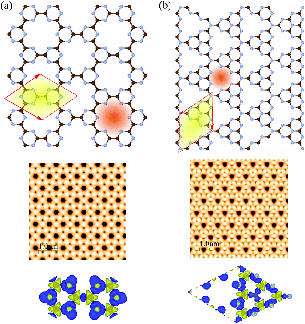 | ||
| Fig. 1 Atomic structures (top), simulated STM images (middle) and charge density differences (bottom) of (a) C6N6 and (b) C6N8 monolayers. The primitive unit cells are indicated by red parallelograms. The brown and blue atoms represent C and N atoms, respectively. The blue and yellow regions represent the charge accumulation and depletion regimes, respectively. | ||
 | ||
| Fig. 2 Electronic band structure (left), density of states and partial density of states (right) of (a) C6N6 and (b) C6N8 monolayers. The insets represent the charge densities of the VBM and CBM. Zero energy is set at the Fermi level. | ||
The optimized lattice constant of monolayer C6N8 is found to be 7.14 Å, with two inequivalent C–N bonds (1.414 and 1.455 Å). In addition, the ring is not a regular hexagon since the C–N–C angle is equal to 120°, while the N–C–N angles are 118° and 122°, respectively. It is clear that every six C–N hexagon rings enclose a nanopore, while the edges are surrounded by six N atoms, with a nanopore diameter of 4.773 Å (see Fig. 2(b)), which is in agreement with previous reports.39,101,104,105 The electronic structure of C6N8 exhibits an indirect semiconductor with a 1.22 eV band gap, which is in agreement with the previous result.106 In addition, from the PDOS of C6N8 it can be clearly seen that the VBM is determined by the N s and px,y orbitals; however, the CBM originates from the N/C pz orbitals.
3.2 Doping of atom into holey site
Here, we discuss the effect of atom doping on the structural and electronic properties of C6N6 and C6N8 monolayers. A 2 × 2 × 1 supercell of C6N6 and C6N8 contains 49 and 57 atoms, respectively. A schematic view of the doped atom in the holey site of the C6N6 and C6N8 monolayers is shown in the ESI, Fig. S1.† For the different atoms considered in our present study, the stable binding sites are uniformly at the nanopore. Through the rest of the study, the atom-doped C6N6 structure is labeled as atom@C6N6. For instance, Mg doped C6N6 is labeled Mg@C6N6.The optimized structures of Mg@, Ca@ and Cr@C6N6 are shown in Fig. 3(a–c), respectively. The Mg and Ca atoms interact through sp2-hybridization and form two and six σ bonds with the neighboring N atoms, respectively. Our results show that the bond lengths of the Mg and Ca atoms with the nearest N atoms are 2.62 and 2.37 Å, respectively (see Table 1). The Cr atom binds to the two nearest N atoms facing the nanopore of the C6N6 monolayer with a bond length of 1.94 Å. Notably, upon atom doping, the planar structure of monolayer C6N6 is preserved. The charge density differences are presented in Fig. 3, where the bond formation, charge accumulation, and depletion regions can clearly be seen. The blue and yellow regions represent charge accumulation and depletion, respectively. For the stability of the structures, we calculate the binding energy (Eb) between the doped atoms and the C6N6/C6N8 sheets by the following formula:
| Eb = Etot − Esheet − Eatom | (1) |
 | ||
| Fig. 3 Optimized structures of (a) Mg, (b) Ca, and (c) Cr atom doped C6N6. (d and e) Optimized structures of C and Ca doped C6N8. Charge density differences are shown in the bottom panel. Blue and yellow regions represent charge accumulation and depletion, respectively. | ||
| Atom | dAN (Å) | dNC (Å) | dCC (Å) | ΔQ (e) | Mtot (μB) | ES |
|---|---|---|---|---|---|---|
| C | 1.46 (1.39) | 1.40 (1.44) | 1.42 (1.42) | 0.99 (1.38) | 0 (0) | SC (SC) |
| Mg | 2.16 (2.30) | 1.39 (1.41) | 1.44 (1.44) | 0.99 (1.38) | 0 (0) | SC (M) |
| Ca | 2.66 (2.37) | 1.38 (1.38) | 1.43 (1.44) | 1.17 (1.32) | 0 (1) | M (FM) |
| Cr | 1.94 (2.16) | 1.41 (1.40) | 1.42 (1.42) | 0.56 (0.63) | 2.4 (2.1) | FM (HM) |
The electronic structures of Mg@, Ca@ and Cr@C6N6 are shown in Fig. 4(a–c), where the solid blue and dashed red lines represent ↑ and ↓ spin channels, respectively. Our results show that in comparison with pristine C6N6, the band structures are modified and give rise to localized mid-gap states arising from the atomic doping. Note that the doping of Mg and Cr atoms gives rise to some localized states in the band structure, which modify the electronic properties. Our results show that Mg@C6N6 exhibits direct band gap semiconducting behavior, with a small band gap of 100 meV where the VBM and CBM are located at the Γ point. Interestingly, we can see that the Ca@C6N6 monolayer exhibits metallic character. In contrast, Cr@C6N6 is a ferromagnetic metal with a net magnetic moment of 2.4 μB. Note that the energy bands of the ↑ and ↓ spin channels near the Fermi-level cross together near to the Dirac-point. On the other hand, monolayer C@C6N8 becomes a direct band gap semiconductor with a narrow band gap of 25 meV, with the VBM and CBM located at the M point. With Ca atom doping in C6N8, we see a spin-polarized ferromagnetic metal with impurity levels crossing the Fermi-level and inducing a net magnetic moment of 1 μB per formula unit. The atomic contributions to the electronic states can be further seen by the PDOS, which are presented in Fig. 5. It is clear that the Mg and Ca states in C6N6 mostly contribute to the deep valence and conduction states. On the other hand, Cr in C6N6 and C in C6N8 also contribute to the states around the Fermi-level. The optimized structures and electronic structures of C@C6N6, Mg@C6N8 and Cr@C6N8 are shown in Fig. S2(a–c),† respectively. We found that the C atoms interact through sp2-hybridization and form two σ bonds with the neighboring N atoms of C6N6. The C@C6N6 structure shows semiconductor behavior with an indirect band gap of 1 eV, where the VBM and CBM are located at the K and M points, respectively (see Fig. S2(a)†). Our results show that the Cr atom bonds to the N host atoms of C6N8 and forms six σ bonds, while the neighboring N atoms of C6N8 form four σ bonds with the Mg atom (see Fig. S2(a) and (b)†). From the electronic band structure, we can see that Mg@C6N8 turns into a metal, whereas the Cr@C6N8 structure becomes a half-metal and a magnetic moment of about 2.1 μB is induced.
 | ||
| Fig. 4 Electronic structures of (a) Mg@C6N6, (b) Ca@C6N6, (c) Cr@C6N6, (d) C@C6N8 and (e) Ca@C6N8. The energy bands of ↑ and ↓ spin channels are indicated by blue lines and red dashed lines, respectively. Zero energy is set at the Fermi-level. | ||
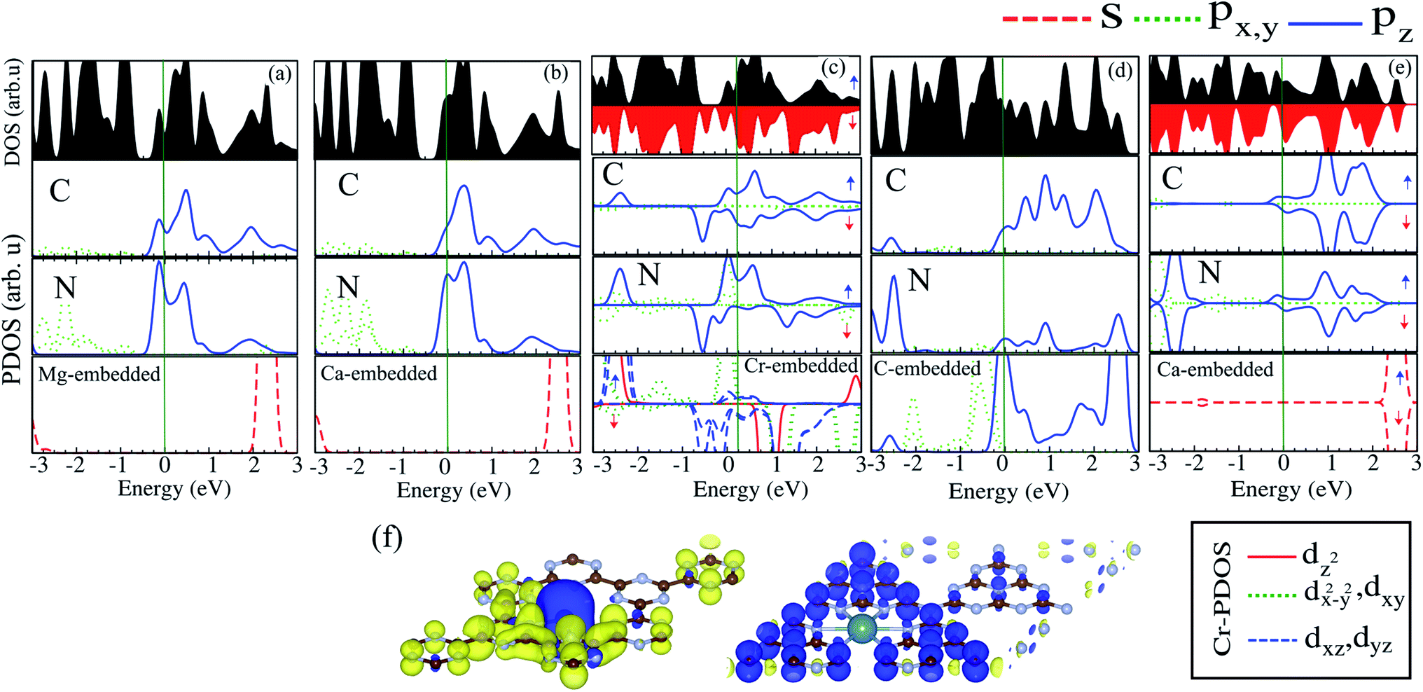 | ||
| Fig. 5 DOS and PDOS of (a) Mg@C6N6, (b) Ca@C6N6, (c) Cr@C6N6, (d) C@C6N8 and (e) Ca@C6N8. (f) Spin density difference. The blue and yellow regions represent the ↑ and ↓ spin states, respectively. | ||
4 Effect of strain
Strain engineering is a robust method to tune the electronic properties and topological nature. In the following, we investigate the effects of uniaxial tensile and compressive strains on the electronic properties of atom doped C6N6 and C6N8 monolayers. The strain is defined as:107 ε = (a ± a0)/a0 × 100, where a and a0 are the strained and non-strained lattice constants, respectively, and the positive (negative) sign denotes tensile (compressive) strain. The band structures of Cr@, Mg@ and Ca@C6N6, and C@ and Ca@C6N8 as a function of the applied strain are shown in Fig. 6(a–e). Cr@C6N6 displays dilute magnetic semiconductor behavior under +2% tensile strain and it is preserved up to +8% strain. In addition, the magnetic moment increases from 2.8 (at −2%) to 3 μB (at −8%) with increasing compressive strain, while it is almost constant under tensile strain. Interestingly, when the compression strain reaches −2%, Cr@C6N6 exhibits spin-polarized semi-metal characteristics. | ||
| Fig. 6 Electronic band structure of (a) Cr@C6N6, (b) Mg@C6N6, (c) Ca@C6N6, (d) C@C6N8 and (e) Ca@C6N8 as a function of strain. The energy bands of ↑ and ↓ spin channels are indicated by blue lines and red dashed lines, respectively. Zero energy is set at the Fermi-level. | ||
Our results show that Mg@C6N6 in the range of −2% to −6% exhibits a decreasing band gap from 90 meV to 70 meV, respectively, while in the strain-free case the band gap is 110 meV. This situation differs under tensile strain, such that the band gap changes in the range of 130 meV to 115 meV. Interestingly, at a tensile strain larger than +8%, the band structure of Mg@C6N6 in both ↑ and ↓ spin channels becomes spin-polarized, leading to the transition from nonmagnetic to magnetic states (see Fig. 6(b)). Ca@C6N6 is naturally a metal; surprisingly, with strains of −2% and −4% the band gaps reach 25 meV and 23 meV, respectively (see Fig. 6(c)), whereas under strain larger than −6% it transforms into a metal and we see a nontrivial band gap of 30 meV in the vicinity of the Fermi-energy. On the other hand, for monolayer Ca@C6N6 under +6 and +8% strain, the VBM (CBM) of the ↓ (↑) spin channel continuously shifts upward (downward) to the Fermi level, resulting in ferromagnetic metallic behavior with magnetic moments of 0.8 μB (+6%) and 1.8 μB (+8%). The electronic band structure of C@C6N8 under strain is shown in Fig. 6(d). C@C6N8 is initially a direct semiconductor with a narrow band gap of 30 meV; however, under 0% ≤ tensile strain ≤ +8%, the band gap increases monotonically from 70 meV (at +2%) to 200 meV (at +8%), while the VBM and CBM of the direct band gap are located at the M point. Our results show that the semiconducting characteristics are preserved in the range of +2% to +8%. Interestingly, C@C6N8 under compression strains of −2, −4 and −8% exhibits semi-metal behavior. When it reaches −6%, it transforms to a metal due to the CBM decrease and VBM increase to the Fermi-level. The electronic band structure of Ca@C6N8 under uniaxial strain in the ↑ and ↓ spin channels is shown in Fig. 6(e). We can see that variations in the magnetic moment occur when it is subjected to tensile and compressive strain. Ca@C6N8 is initially a ferromagnetic metal with a magnetic moment of 1 μB in the ground state. Interestingly, when a strain larger than +2% to +8% is applied, the ferromagnetic metal state is lost and both the ↑ and ↓ spin channels become non-spin-polarized, leading to a transition from a ferromagnetic metal to a nonmagnetic-metal state. Note that by increasing strain up to +2%, its magnetic moment vanishes. Also, for strains of 2–4%, Ca@C6N8 transforms into a nonmagnetic metal, while for larger strains (>−6%) the structure transforms into a ferromagnetic metal with magnetic moments of 0.47 μB (−6%) and 0.53 μB (−8%).
The electronic structures of Cr@C6N6 without strain and with −2% strain, considering spin–orbital coupling (SOC) and without SOC, are shown in Fig. 7(a) and (b). For Cr@C6N6 upon −2% compression strain, without considering SOC, we can see that the ↑ and ↓ spin bands cross each other at the Fermi-level, which implies a magnetic semi-metallic nature. Our results show that when the SOC effect is considered, we see a touching point along the Γ and K paths at the Fermi level, and a narrow band gap of 125 meV forms in the proximity of the Fermi level, which implies a semi-metallic character. The effect of SOC correction on the evolution of electronic structure was found to be remarkable, such that degeneracies at the VBM are removed. Due to weak screening of the Coulomb interaction in the doping of transition metal atoms, the Hubbard U energy band structure may be expected to be weak. Since the accurate value of U has not been determined, we investigate the correlation effects by the value of the Hubbard U. To confirm that semi-metallicity is not an artificial result from the GGA+U method, we perform calculations for the doping of Cr atoms. The electronic band structures of Cr@C6N6 without strain and with −2% strain, without (left) and with consideration of the Hubbard U effect (right) are shown in Fig. S3(a) and (b),† respectively. The correlation effects on the electronic and magnetic properties of Cr@C6N6 without and with strain are significant and cause changes in the spin polarization. In the Cr-doped C6N6 without strain and upon −2% compression strain, we can see that the ↑ and ↓ spin bands cross each other at the Fermi-level, which implies a spin-polarized semi-metallic nature, without considering Hubbard U. We can see that a nodal-line forms around the K and M points when U = 2 eV is considered. Our results show that the magnetic moment of Cr@C6N6 in U = 2 eV are 3.53 μB (without strain) and 3.63 μB (with −2% strain).
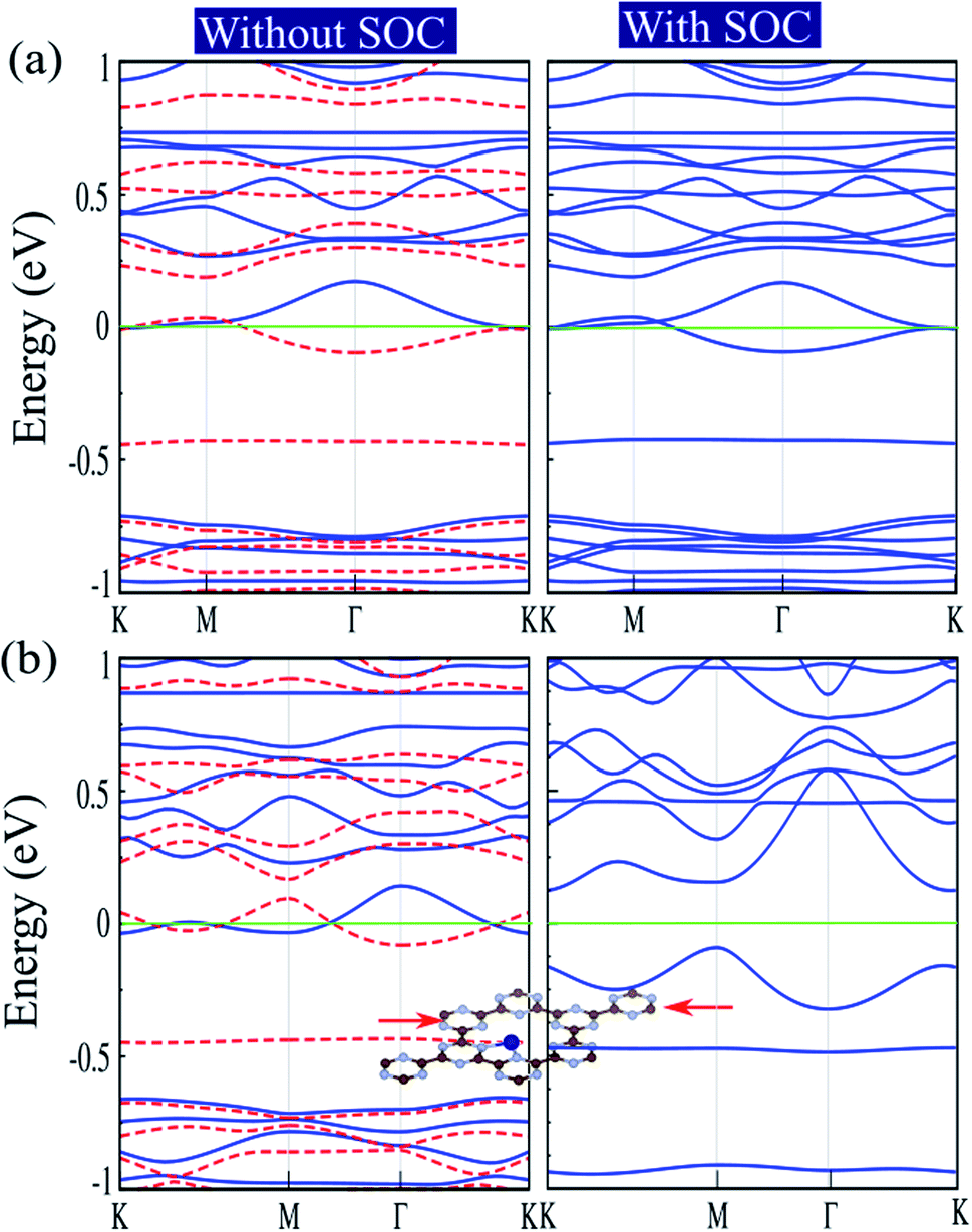 | ||
| Fig. 7 Electronic structures of (a) Cr@C6N6, without and with consideration of spin–orbital coupling (SOC) effect; (b) Cr@C6N6 upon −2% strain, without and with SOC effect. Optimized structures under the applied strain are shown in the insets. The energy bands of ↑ and ↓ spin channels are indicated by blue lines and red dashed lines, respectively. Zero energy is set at the Fermi-level. | ||
Here, we discuss the magnetic coupling between Cr–Cr doped in C6N6 monolayers. We consider two Cr atoms doped in one and two neighboring cavities for comparison. The spin density differences of Cr doped in one and two neighboring cavities of C6N6 are shown in Fig. S4.† The electronic band structures are indicated in the right panels. All of the possible relative positions of two Cr atoms doped in one and two cavities of C6N6 are considered, and only the most stable configurations are exhibited. The exchange energy Eex, defined as Eex = EFM − EAFM, is calculated to determine the most stable phase. Negative and positive Eex indicate the FM and AFM ground states, respectively. For the case of one neighboring cavity, it is found that the Cr atoms exhibit FM coupling (with Eex = 140 meV) in their most stable phases, and the corresponding spin density differences are shown in Fig. S4(a).† Because the distance between the two Cr atoms is small (∼1.82 Å), one may think that the two Cr atoms should show direct coupling through C/N atoms. For the case of two cavities, it is clearly seen that the case of the Cr atoms is quite different from the above findings and they show AFM coupling (Eex = 30 meV) with corresponding spin density differences.
5 Conclusion
In summary, using first-principles calculations, we have explored the effects of atom doping on the structural, electronic, and magnetic properties of C6N6 and C6N8 monolayers. Our theoretical results indicated that with atom doping, C6N6 becomes a semiconductor with a narrow band gap (Mg-doped), semi-metal (Ca-doped) or ferromagnetic metal (Cr-doped). Additionally, we applied mechanical strain to both monolayers with atoms doped in their lattices. Our first-principles results revealed that the band gap and magnetism can be finely tuned by strain as well. Surprisingly, when the compressive strain reaches 2%, Cr-doped C6N6 displays a phase transition to a spin-polarized semi-metal without SOC; when SOC is considered, a narrow band gap of 125 meV is opened. Notably, in the case of Cr atom doped C6N6 upon compressive strain, considering SOC, an unusual semi-metallic character can be observed. In the C-doped C6N8 between applied tensile strains of 0–8%, the band gap was found to increase monotonically from 70 meV (at 2%) to 200 meV (at 8%), while it exhibits semi-metallic behavior under compressive strain larger than 2%. Our results show that a magnetic-to-nonmagnetic phase transition can occur under large tensile strain in the Ca doped C6N8 monolayer. In addition, Mg and Ca atom doped C6N6 can show topological insulator states under strain. The results provided by our extensive theoretical analysis highlight very promising electronic properties of C6N6 and C6N8 monolayers doped with various atoms and under mechanical strain, and will hopefully serve as a guide for future experimental and theoretical studies.Conflicts of interest
The authors declare that there are no conflicts of interest regarding the publication of this paper.Acknowledgements
This work was supported by the National Research Foundation of Korea (NRF) grant funded by the Korean government (MSIT) (NRF-2017R1A2B2011989).References
- A. Wang, X. Zhang and M. Zhao, Nanoscale, 2014, 6, 11157–11162 RSC
.
- Y. Z. Abdullahi, T. L. Yoon, M. M. Halim, M. R. Hashim and T. L. Lim, Solid State Commun., 2016, 248, 144–150 CrossRef CAS
- A. Du, S. Sanvito and S. C. Smith, Phys. Rev. Lett., 2012, 108, 197207 CrossRef PubMed
- G. Wang, X. Long, K. Qi, S. Dang, M. Zhong, S. Xiao and T. Zhou, Appl. Surf. Sci., 2019, 471, 162–167 CrossRef CAS
- G. Wang, F. Zhou, B. Yuan, S. Xiao, A. Kuang, M. Zhong, S. Dang, X. Long and W. Zhang, Nanomaterials, 2019, 9, 244 CrossRef CAS PubMed
- X. Zhao, D. Pan, X. Chen, R. Li, T. Jiang, W. Wang, G. Li and D. Y. Leung, Appl. Surf. Sci., 2019, 467–468, 658–665 CrossRef CAS
- G.-C. Guo, R.-Z. Wang, B.-M. Ming, C. Wang, S.-W. Luo, C. Lai and M. Zhang, Appl. Surf. Sci., 2019, 475, 102–108 CrossRef CAS
- X. Gao, Y. Shen, Y. Ma, S. Wu and Z. Zhou, Appl. Surf. Sci., 2019, 479, 1098–1104 CrossRef CAS
- Y. Yong, H. Cui, Q. Zhou, X. Su, Y. Kuang and X. Li, Appl. Surf. Sci., 2019, 487, 488–495 CrossRef CAS
- L.-B. Shi, M. Yang, S. Cao, Q. You, Y.-Y. Niu and Y.-Z. Wang, Appl. Surf. Sci., 2019, 492, 435–448 CrossRef CAS
- Q. H. Wang, K. Kalantar-Zadeh, A. Kis, J. N. Coleman and M. S. Strano, Nat. Nanotechnol., 2012, 7, 699 CrossRef CAS PubMed
- X.-H. Li, X. Wang and M. Antonietti, Chem. Sci., 2012, 3, 2170–2174 RSC
- J. Zhang, M. Grzelczak, Y. Hou, K. Maeda, K. Domen, X. Fu, M. Antonietti and X. Wang, Chem. Sci., 2012, 3, 443–446 RSC
- X. Zhang, X. Xie, H. Wang, J. Zhang, B. Pan and Y. Xie, J. Am. Chem. Soc., 2013, 135, 18–21 CrossRef CAS PubMed
- X. Zhang, H. Wang, H. Wang, Q. Zhang, J. Xie, Y. Tian, J. Wang and Y. Xie, Adv. Mater., 2014, 26, 4438–4443 CrossRef CAS PubMed
- B. Zhu, L. Zhang, B. Cheng and J. Yu, Appl. Catal., B, 2018, 224, 983–999 CrossRef CAS
- A. Bafekry, S. Farjami Shayesteh and F. M. Peeters, J. Phys. Chem. C, 2019, 123, 12485–12499 CrossRef CAS
- A. Bafekry and M. Neek-Amal, Phys. Rev. B, 2020, 101, 085417 CrossRef CAS
- A. Bafekry, S. F. Shayesteh and F. M. Peeters, Phys. Chem. Chem. Phys., 2019, 21, 21070–21083 RSC
- A. Bafekry, M. Ghergherehchi, S. F. Shayesteh and F. Peeters, Chem. Phys., 2019, 526, 110442 CrossRef CAS
- A. Bafekry, C. Stampfl and S. Farjami Shayesteh, ChemPhysChem, 2020, 21, 164–174 CrossRef CAS PubMed
- Q. Zhou, M. Wu, M. Zhang, G. Xu, B. Yao, C. Li and G. Shi, Materials Today Energy, 2017, 6, 181–188 CrossRef
- S. U. Lee, R. V. Belosludov, H. Mizuseki and Y. Kawazoe, Small, 2009, 5, 1769–1775 CrossRef CAS PubMed
- J. Li, W. Cui, Y. Sun, Y. Chu, W. Cen and F. Dong, J. Mater. Chem. A, 2017, 5, 9358–9364 RSC
- Y. Zheng, J. Liu, J. Liang, M. Jaroniec and S. Z. Qiao, Energy Environ. Sci., 2012, 5, 6717–6731 RSC
- A. Thomas, A. Fischer, F. Goettmann, M. Antonietti, J.-O. Müller, R. Schlögl and J. M. Carlsson, J. Mater. Chem., 2008, 18, 4893–4908 RSC
- G. Algara-Siller, N. Severin, S. Y. Chong, T. Björkman, R. G. Palgrave, A. Laybourn, M. Antonietti, Y. Z. Khimyak, A. V. Krasheninnikov and J. P. Rabe, et al., Angew. Chem., Int. Ed., 2014, 53, 7450–7455 CrossRef CAS PubMed
- J. Mahmood, E. K. Lee, M. Jung, D. Shin, I.-Y. Jeon, S.-M. Jung, H.-J. Choi, J.-M. Seo, S.-Y. Bae and S.-D. Sohn, et al., Nat. Commun., 2015, 6, 6486 CrossRef CAS PubMed
- M. Groenewolt and M. Antonietti, Adv. Mater., 2005, 17, 1789–1792 CrossRef CAS
- J. S. Lee, X. Wang, H. Luo and S. Dai, Adv. Mater., 2010, 22, 1004–1007 CrossRef CAS PubMed
- Y. Xu and S.-P. Gao, Int. J. Hydrogen Energy, 2012, 37, 11072–11080 CrossRef CAS
- V. N. Khabashesku, J. L. Zimmerman and J. L. Margrave, Chem. Mater., 2000, 12, 3264–3270 CrossRef CAS
- B. Yang, H. Zhou, X. Zhang and M. Zhao, J. Mater. Chem. C, 2015, 3, 10886–10891 RSC
- Q. Guo, Q. Yang, C. Yi, L. Zhu and Y. Xie, Carbon, 2005, 43, 1386–1391 CrossRef CAS
- J. Li, C. Cao, J. Hao, H. Qiu, Y. Xu and H. Zhu, Diamond Relat. Mater., 2006, 15, 1593–1600 CrossRef CAS
- H. Qiu, Z. Wang and X. Sheng, Phys. Lett. A, 2013, 377, 347–350 CrossRef CAS
- G.-X. Chen, D.-D. Wang, J.-Q. Wen, A.-P. Yang and J.-M. Zhang, Int. J. Quantum Chem., 2016, 116, 1000–1005 CrossRef CAS
- D. Ghosh, G. Periyasamy, B. Pandey and S. K. Pati, J. Mater. Chem. C, 2014, 2, 7943–7951 RSC
- I. Choudhuri, G. Bhattacharyya, S. Kumar and B. Pathak, J. Mater. Chem. C, 2016, 4, 11530–11539 RSC
- I. Choudhuri, P. Garg and B. Pathak, J. Mater. Chem. C, 2016, 4, 8253–8262 RSC
- X. Jiang, P. Wang and J. Zhao, J. Mater. Chem. A, 2015, 3, 7750–7758 RSC
- S. Yang, W. Li, C. Ye, G. Wang, H. Tian, C. Zhu, P. He, G. Ding, X. Xie and Y. Liu, et al., Adv. Mater., 2017, 29, 1605625 CrossRef PubMed
- H. Li, H. Hu, C. Bao, F. Guo, X. Zhang, X. Liu, J. Hua, J. Tan, A. Wang and H. Zhou, et al., Sci. Rep., 2016, 6, 29327 CrossRef CAS PubMed
- H. Li, H. Hu, C. Bao, Z. Feng, F. Guo, G. Tian and Y. Liu, Diamond Relat. Mater., 2018, 87, 50–55 CrossRef CAS
- H. Li, H. Hu, C. Bao, J. Hua, H. Zhou, X. Liu, X. Liu and M. Zhao, Phys. Chem. Chem. Phys., 2015, 17, 6028–6035 RSC
- E. Kroke, M. Schwarz, E. Horath-Bordon, P. Kroll, B. Noll and A. D. Norman, New J. Chem., 2002, 26, 508–512 RSC
- J. Sehnert, K. Baerwinkel and J. Senker, J. Phys. Chem. B, 2007, 111, 10671–10680 CrossRef CAS PubMed
- J. N. Hart, F. Claeyssens, N. L. Allan and P. W. May, Phys. Rev. B: Condens. Matter Mater. Phys., 2009, 80, 174111 CrossRef
- A. Snis and S. F. Matar, Phys. Rev. B: Condens. Matter Mater. Phys., 1999, 60(15), 10855 CrossRef CAS
- P. Esquinazi, D. Spemann, R. Höhne, A. Setzer, K.-H. Han and T. Butz, Phys. Rev. Lett., 2003, 91, 227201 CrossRef CAS PubMed
- K. W. Lee and C. E. Lee, Phys. Rev. Lett., 2006, 97, 137206 CrossRef PubMed
- P. O. Lehtinen, A. S. Foster, Y. Ma, A. Krasheninnikov and R. M. Nieminen, Phys. Rev. Lett., 2004, 93, 187202 CrossRef CAS PubMed
- J. Zhou, Q. Wang, Q. Sun, X. Chen, Y. Kawazoe and P. Jena, Nano Lett., 2009, 9, 3867–3870 CrossRef CAS PubMed
- Q.-F. Deng, L. Liu, X.-Z. Lin, G. Du, Y. Liu and Z.-Y. Yuan, Chem. Eng. J., 2012, 203, 63–70 CrossRef CAS
- A. Bafekry, C. Stampfl, M. Ghergherehchi and S. F. Shayesteh, Carbon, 2020, 157, 371–384 CrossRef CAS
- A. Bafekry, S. Farjami Shayesteh, M. Ghergherehchi and F. M. Peeters, J. Appl. Phys., 2019, 126, 144304 CrossRef
- M. M. Obeid, Appl. Surf. Sci., 2020, 508, 144824 CrossRef
- A. Bafekry, C. Stampfl, B. Akgenc and M. Ghergherehchi, Phys. Chem. Chem. Phys., 2020, 22, 2249–2261 RSC
- M. Yagmurcukardes, C. Sevik and F. Peeters, Phys. Rev. B, 2019, 100, 045415 CrossRef CAS
- A. Bafekry, S. F. Shayesteh and F. M. Peeters, J. Appl. Phys., 2019, 126, 215104 CrossRef
- D. Kiymaz, M. Yagmurcukardes, A. Tomak, H. Sahin, R. T. Senger, F. M. Peeters, H. M. Zareie and C. Zafer, Nanotechnology, 2016, 27, 455604 CrossRef CAS PubMed
- A. Bafekry, Phys. E, 2020, 118, 113850 CrossRef CAS
- F. İyikanat, M. Yagmurcukardes, R. T. Senger and H. Sahin, J. Mater. Chem. C, 2018, 6, 2019–2025 RSC
- A. Bafekry, C. Stampfl, B. Akgenc, B. Mortazavi, M. Ghergherehchi and C. V. Nguyen, Phys. Chem. Chem. Phys., 2020, 22, 6418–6433 RSC
- A. Bafekry, B. Akgenc, S. F. Shayesteh and B. Mortazavi, Appl. Surf. Sci., 2020, 505, 144450 CrossRef
- A. Kasry, M. M. Fadlallah, N. H. Voelcker and A. A. Maarouf, Carbon, 2019, 155, 65–70 CrossRef CAS
- M. Fadlallah, M. Shibl, T. Vlugt and U. Schwingenschlögl, J. Mater. Chem. A, 2018, 6, 24342–24349 RSC
- A. Bafekry and M. Neek-Amal, Phys. Rev. B, 2020, 101, 085417 CrossRef CAS
- Z. Kahraman, A. Kandemir, M. Yagmurcukardes and H. Sahin, J. Phys. Chem. C, 2019, 123, 4549–4557 CrossRef CAS
- A. Bafekry, C. Stampfl and F. M. Peeters, Sci. Rep., 2020, 10, 1–15 CrossRef PubMed
- M. Yagmurcukardes, S. Ozen, F. Iyikanat, F. Peeters and H. Sahin, Phys. Rev. B, 2019, 99, 205405 CrossRef CAS
- B. Mortazavi, A. Bafekry, M. Shahrokhi, T. Rabczuk and X. Zhuang, Materials Today Energy, 2020, 16, 100392 CrossRef
- M. M. Fadlallah and U. Eckern, Phys. Status Solidi B, 2020, 257, 1900217 CrossRef CAS
- M. M. Obeid, H. R. Jappor, K. Al-Marzoki, D. Hoat, T. V. Vu, S. J. Edrees, Z. M. Yaseen and M. M. Shukur, Comput. Mater. Sci., 2019, 170, 109201 CrossRef CAS
- A. Bafekry, M. Ghergherehchi and S. F. Shayesteh, Phys. Chem. Chem. Phys., 2019, 21, 10552–10566 RSC
- H. R. Jappor, M. M. Obeid, T. V. Vu, D. Hoat, H. D. Bui, N. N. Hieu, S. J. Edrees, Y. Mogulkoc and R. Khenata, Superlattices Microstruct., 2019, 130, 545–553 CrossRef CAS
- A. Bafekry, B. Mortazavi and S. F. Shayesteh, J. Magn. Magn. Mater., 2019, 491, 165565 CrossRef CAS
- M. Shahrokhi and C. Leonard, J. Alloys Compd., 2017, 693, 1185–1196 CrossRef CAS
- A. Bafekry, C. Stampfl and F. M. Peeters, Phys. Status Solidi B, 2020, 257, 2000182 CrossRef CAS
- M. Fadlallah, Phys. E, 2017, 89, 50–56 CrossRef CAS
- M. S. Eldeeb, M. M. Fadlallah, G. J. Martyna and A. A. Maarouf, Carbon, 2018, 133, 369–378 CrossRef CAS
- A. Bafekry, B. Akgenc, M. Ghergherehchi and F. Peeters, J. Phys.: Condens. Matter, 2020, 32, 355504 CrossRef CAS PubMed
- M. Shahrokhi and C. Leonard, J. Alloys Compd., 2016, 682, 254–262 CrossRef CAS
- F. Shojaei, M. Azizi, Z. Mahdavifar, B. Wang and G. Frapper, RSC Adv., 2020, 10, 8016–8026 RSC
- M. Shahrokhi, Diamond Relat. Mater., 2017, 77, 35–40 CrossRef CAS
- A. Bafekry, M. Yagmurcukardes, B. Akgenc, M. Ghergherehchi and C. V. Nguyen, J. Phys. D: Appl. Phys., 2020, 53, 355106 CrossRef
- B. Mortazavi, F. Shojaei, M. Azizi, T. Rabczuk and X. Zhuang, J. Mater. Chem. C, 2020, 8, 2400–2410 RSC
- A. Bafekry, C. Stampfl and M. Ghergherehchi, Nanotechnology, 2020, 31, 295202 CrossRef CAS PubMed
- F. Shojaei, B. Mortazavi, X. Zhuang and M. Azizi, Materials Today Energy, 2020, 16, 100377 CrossRef
- A. Bafekry, M. Neek-Amal and F. Peeters, Phys. Rev. B, 2020, 101, 165407 CrossRef CAS
- T. Ozaki, K. Nishio and H. Kino, Phys. Rev. B: Condens. Matter Mater. Phys., 2010, 81, 035116 CrossRef
- T. Ozaki, Phys. Rev. B: Condens. Matter Mater. Phys., 2003, 67, 155108 CrossRef
- T. Ozaki and H. Kino, Phys. Rev. B: Condens. Matter Mater. Phys., 2004, 69, 195113 CrossRef
- J. P. Perdew, K. Burke and M. Ernzerhof, Phys. Rev. Lett., 1996, 77, 3865 CrossRef CAS PubMed
- N. Troullier and J. L. Martins, Phys. Rev. B: Condens. Matter Mater. Phys., 1991, 43, 1993 CrossRef CAS PubMed
- H. J. Monkhorst and J. D. Pack, Phys. Rev. B: Solid State, 1976, 13, 5188 CrossRef
- T. Bucko, J. Hafner, S. Lebegue and J. G. Angyán, J. Phys. Chem. A, 2010, 114, 11814–11824 CrossRef CAS PubMed
- R. Mulliken, J. Chem. Phys., 1955, 23, 2343–2346 CrossRef CAS
- J. Tersoff and D. Hamann, Phys. Rev. Lett., 1983, 50, 1998 CrossRef CAS
- I. Horcas, R. Fernández, J. Gomez-Rodriguez, J. Colchero, J. Gómez-Herrero and A. Baro, Rev. Sci. Instrum., 2007, 78, 013705 CrossRef CAS PubMed
- X. Wang, K. Maeda, A. Thomas, K. Takanabe, G. Xin, J. M. Carlsson, K. Domen and M. Antonietti, Nat. Mater., 2009, 8, 76–80 CrossRef CAS PubMed
- G. Liu, P. Niu, C. Sun, S. C. Smith, Z. Chen, G. Q. Lu and H.-M. Cheng, J. Am. Chem. Soc., 2010, 132, 11642–11648 CrossRef CAS PubMed
- K. Srinivasu, B. Modak and S. K. Ghosh, J. Phys. Chem. C, 2014, 118, 26479–26484 CrossRef CAS
- Q. Zhang, Y. Cheng, L.-Y. Gan and U. Schwingenschlögl, Phys. Rev. B: Condens. Matter Mater. Phys., 2013, 88, 245447 CrossRef
- J. Wirth, R. Neumann, M. Antonietti and P. Saalfrank, Phys. Chem. Chem. Phys., 2014, 16, 15917–15926 RSC
- X. Li, Y. Dai, Y. Ma, S. Han and B. Huang, Phys. Chem. Chem. Phys., 2014, 16, 4230–4235 RSC
- H. Li, H. Hu, C. Bai, C. Bao, F. Guo, Z. Feng and Y. Liu, RSC Adv., 2019, 9, 7464–7468 RSC
- A. Bafekry, M. Yagmurcukardes, M. Shahrokhi and M. Ghergherehchi, Carbon, 2020, 168, 220–229 CrossRef CAS
- A. Bafekry, M. M. Obeid, C. V. Nguyen, M. Ghergherehchi and M. B. Tagani, J. Mater. Chem. A, 2020, 8, 13248–13260 RSC
- M. Rassekh, J. He, S. F. Shayesteh and J. J. Palacios, Comput. Mater. Sci., 2020, 183, 109820 CrossRef CAS
Footnote |
| † Electronic supplementary information (ESI) available. See DOI: 10.1039/d0ra04463f |
| This journal is © The Royal Society of Chemistry 2020 |