
 Open Access Article
 This Open Access Article is licensed under a Creative Commons Attribution-Non Commercial 3.0 Unported Licence
Solution-processable and photopolymerisable TiO2 nanorods as dielectric layers for thin film transistors†
Fei Chenga,
Emanuele Verrellib,
Fahad A. Alharthi ac,
Satyajit Dasd,
Thomas D. Anthopoulosde,
Khue T. Laif,
Neil T. Kempb,
Mary O'Neillg and
Stephen M. Kelly*a
ac,
Satyajit Dasd,
Thomas D. Anthopoulosde,
Khue T. Laif,
Neil T. Kempb,
Mary O'Neillg and
Stephen M. Kelly*a
aDepartment of Chemistry & Biochemistry, University of Hull, Cottingham Road, Hull, HU6 7RX, UK. E-mail: s.m.kelly@hull.ac.uk
bDepartment of Physics & Mathematics, University of Hull, Cottingham Road, Hull, HU6 7RX, UK
cDepartment of Chemistry, College of Science, King Saud University, P. O. Box 2455, Riyadh 11451, Saudi Arabia
dCentre for Plastic Electronics, Department of Physics, Blackett Laboratory, Imperial College London, London SW7 2BW, UK
eKing Abdullah University of Science and Technology (KAUST), KAUST Solar Centre, Thuwal 23955-6900, Saudi Arabia
fElectronic Systems Design Centre, Energy Safety Research Institute, College of Engineering, Swansea University Bay Campus, Swansea, SA1 8EN, UK
gSchool of Science & Technology, Nottingham Trent University, 50 Shakespeare Street, Nottingham, NG1 3LL, UK
First published on 6th July 2020
Abstract
We report the fabrication of a solution-processed n-type Thin Film Transistor (TFT) with current on/off ratios of 104, a turn-on voltage (VON) of 1.2 V and a threshold voltage (VT) of 6.2 V. The TFT incorporates an insoluble and intractable dielectric layer (k = 7–9) prepared in situ from solution-processed and then photopolymerised ligand-stabilised, inorganic/organic TiO2 nanorods. A solution processed zinc oxide (ZnO) layer acts as the semiconductor. The new surface-modified TiO2 nanorods were synthesised using a ligand replacement process with a monolayer coating of photopolymerisable 10-undecynylphosphonic acid (10UCYPA) to render them both soluble in common organic solvents and be photopolymerisable using UV-illumination after having been deposited on substrate surfaces from solution and drying.
Introduction
Research on solution-processed Thin Film Transistors (TFTs) and Organic Field-Effect Transistors (OFETs) has advanced rapidly in recent years due to the advantages of low-temperature, solution-processing fabrication over large-areas and on flexible, inexpensive and lightweight substrates.1,2 Solution-processed metal-oxide TFTs are attractive due to high charge carrier mobility, good uniformity and transparency at low cost.1 Thin gate insulator films with a high dielectric constant, k, would increase the capacitance and lower the operating voltage of OFETs.2 Whilst some solution-processed inorganic dielectric materials, such as titanium oxide,1,3,4 have been developed, their use has so far been limited in commercial TFTs and OFETs, mostly due to high post-deposition annealing temperatures.1,5 Thus, there is a need to develop new approaches to solution-processed dielectrics based on inorganic semiconductors, such as metal oxides, with low-temperature processing for TFTs and OFETs in plastic electronics.In order to render metal oxide nanoparticles, such as titanium dioxide (TiO2), processable from solution in organic solvents, the nanoparticle surfaces can be functionalised with organic ligands to overcome the strong adhesion forces between them. Ligands with long aliphatic chains are often used to stabilise nanoparticles of sphere- or rod-like inorganic core. Generally, surface modification can be carried out either in situ or as part of post-synthesis modification methods. Under in situ modification, the attachment of the ligands onto nanoparticle surfaces is completed during the growth of nanocrystals.5–7 So far, surface-modification of TiO2 nanoparticles, for example, has been achieved with carboxylic acids,8 mixed carboxylic acids and amines,9 dicarboxylic acids,10 octadecylsilane with different headgroups,11 phosphonic acid and phosphinic esters.12 Ligand-exchange reactions (LER) of polystyrene-capped TiO2 nanoparticles have been reported to yield hybrid, organic/inorganic TiO2 nanoparticles as solution-processable dielectric layers. Unfortunately, the TiO2 nanoparticle content is quite low due to the high polymer content.13
Insoluble thin films can be prepared by ultraviolet irradiation of photopolymerizable materials to form insoluble polymer networks. An example of this approach involves the attachment of a photopolymerisable moiety, such as an acrylate, methacrylate or oxetane group, via an aliphatic spacer to a small molecule organic semiconductor.14–18 A significant advantage of this approach is the capability to spatially pattern device features with sub-micron resolution using photolithography, e.g., organic semiconductors for Organic Light-Emitting Diodes (OLEDs), Organic Photovoltaics (OPVs) and Organic Field-Effect Transistors (OFETs).14–20
Here we report the fabrication of a solution-processed prototype n-type Thin Film Transistor (TFT) incorporating an insoluble and intractable dielectric layer prepared in situ from solution-processed and then photopolymerised ligand-stabilised, inorganic/organic TiO2 nanorods and zinc oxide (ZnO) as the semiconductor, also deposited from solution. The new surface-modified TiO2 nanorods were synthesised using a ligand replacement process with a monolayer coating of photopolymerisable 10-undecynylphosphonic acid (10UCYPA) to render them both soluble in common organic solvents and be photopolymerisable using UV-illumination after having been deposited on substrate surfaces from solution and then drying at moderately low temperatures (100 °C) for a short time (10 min). Hence, we now report the synthesis and processing of solution-processable and photopolymerisable, mixed ligand-stabilized titanium dioxide nanorods using 10-undecynylphosphonic acid (10UCYPA) as a ligand (Scheme 1) using a Ligand Exchange Reaction (LER).21 The presence of a monolayer of this new ligand on the titanium oxide nanorod surfaces is designed to render them soluble in typical organic solvents used to deposit semiconductors from solution, e.g., by spin coating, drop casting, inkjet printing etc. (Scheme, ESI†). A high density of the 10UCYPA ligand should facilitate photopolymerisation of the triple bonds of adjacent ligands to form completely insoluble and intractable thin films on illumination with UV-radiation. We have previously reported that such thin films of ligand-exchanged TiO2 inorganic/organic semiconductors exhibit a dielectric constant, k = 8, high enough to allow them to function as dielectric layers in multilayer plastic electronic devices.21
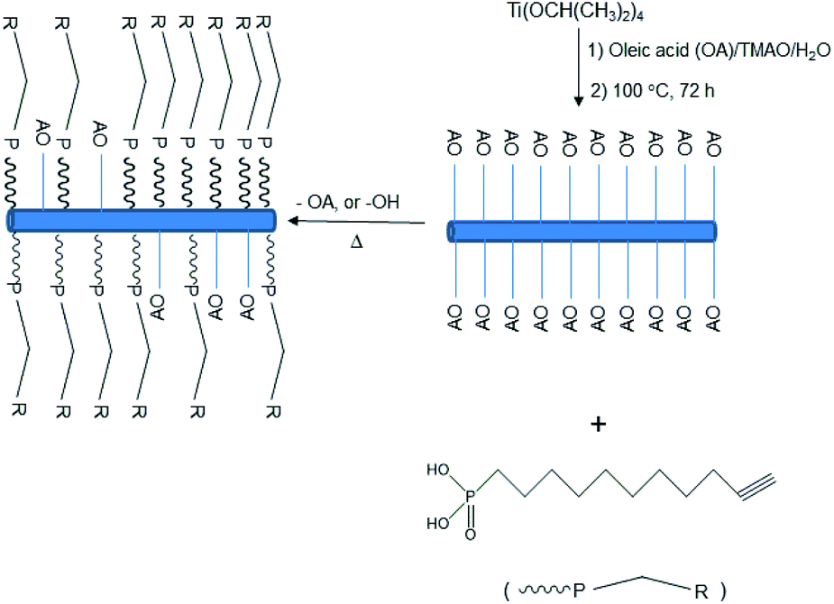 | ||
| Scheme 1 Preparation of mixed ligand-stabilized TiO2 nanorods with 10-undecynylphosphonic acid (10UCYPA) as a ligand exchanger for oleic acid (OA). | ||
Experimental
Materials
Titanium(IV) tetraisopropoxide (TTIP, ≥97.0%), oleic acid (OA, 90%), trimethylamine N-oxide (TMAO, 98%) and chlorobenzene were sourced from Sigma-Aldrich. 10-Undecynylphosphonic acid (10UCYPA, ≥95.0%) was purchased from SiKEMIA, France. Ultrapure water with a specific resistance of 18.2 MΩ cm was obtained by reversed osmosis followed by ion-exchange and filtration (UPQ PS system, ELGA, USA).Synthesis of oleic acid stabilized titanium oxide nanorods (TiO2-OA)
The oleic acid-stabilized TiO2 nanorods (TiO2-OA) were prepared using a modified literature procedure.6,22 Oleic acid (420 g) was dried under vacuum by heating to 120 °C for 1 h to remove water. After that, it was allowed to cool to 85 °C under nitrogen flow. Titanium(IV) isopropoxide (17.7 mL, 60 mmol) was added under stirring whereby the reaction solution took on a yellow colour. After 5 minutes, an aqueous solution of trimethylamine N-oxide (2 M, 60 cm3) was injected quickly using a syringe. The subsequent mixture was heated to 100 °C and reacted for 72 h under stirring and nitrogen flow. Then, the reaction mixture was allowed to cool to room temperature and dried under vacuum to remove water. An excess of isopropanol (1.2 L) was added to the mixture solution, the precipitate was centrifuged and washed twice with isopropanol. The resultant solid was dissolved again in toluene and precipitated with acetone. The precipitate was separated by centrifugation. This purification step was repeated twice. The resultant precipitate was dried overnight in a vacuum oven to yield the desired titanium dioxide nanorods (TiO2-OA) coated with a monolayer of oleic acid ligands (ca. 6.0 g) as a light yellow powder.Ligand exchange of TiO2-OA by 10UCYPA
10-Undecynylphosphonic acid (10UCYPA, 25.0 mg) dissolved in chlorobenzene (2 cm3) was added to a solution of titanium dioxide nanorods (TiO2-OA) coated with a monolayer of oleic acid ligands (100 mg) in chlorobenzene (2 cm3). The resultant mixture was heated at 100 °C for 24 h. The chlorobenzene solvent was removed under vacuum and the solid was dissolved in acetone and then precipitated with hexane to purify the nanocomposites. The desired ligand-exchanged nanocomposite (TiO2-10UCYPA) was then obtained by centrifugation, washed with hexane, and dried in a vacuum oven.Thin films and electronic devices
The hybrid material TiO2-10UCYPA was solution processed and spin coated onto planar glass substrates in order to create smooth uniform thin films with a thickness of 100–300 nm depending on the deposition conditions. The required solutions were prepared by dissolving the nanocomposite (TiO2-10UCYPA) powders in chlorobenzene at concentrations of 10 wt%. Spin coating was carried out at 1000 rpm for 60 s (unless otherwise specified) and the thin films were subsequently baked at 100 °C for 10 min in air to remove excess solvent. In these conditions the film thickness (measured using a Bruker Dektak XT profilometer) was ∼200 nm. The morphology of the films was investigated using an intermittent contact mode AFM (Agilent 5500 AFM system). UV-crosslinking of the thin films was carried out in an inert glove box environment at 1 ppm O2, −86 °C dewpoint using a UV curing lamp (OmniCure 2000, 250–450 nm) with a power density of 1.5 W cm−2. A Bruker IFS 66/S Fourier transform infrared spectrometer equipped with a water-cooled glowbar source, a potassium bromide (KBr) beam splitter and a deuterated triglycine sulphate detector was used to measure the transmittance of the thin films at room temperature. The KBr substrate spectrum was taken under the same conditions as each sample measurement in order to eliminate any inherent artefacts. The resolution was 2 cm−1 and 1000 scans were combined and averaged to produce each FTIR spectrum. The sample compartment was continuously purged with anhydrous air to reduce absorption due to atmospheric water vapour and carbon dioxide.Microscale capacitors with an active area of 10−4 cm2 were fabricated in order to investigate the dielectric properties of the thin films. The capacitors were fabricated in a crossbar approach on glass substrates and comprised a bottom aluminium electrode, the hybrid thin film deposited by spin coating as mentioned above and a top aluminium electrode deposited under high vacuum. Impedance spectra were acquired using a Solartron S1260 with a dielectric interface S1296. Test Thin Film Transistors (TFTs) were fabricated in bottom-contact, top-gate configuration on glass substrates using as a semiconductor ZnO film deposited via spin coating (4000 rpm for 30 s). The S/D contacts and gate electrodes used were aluminium (50 nm-thick) evaporated in vacuum. The precursor solution for ZnO film was formed by dissolving zinc oxide hydrate (ZnO·H2O, 97%, Sigma-Aldrich) in ammonium hydroxide [50% (v/v) aqueous solution, Alfa Aesar] at a concentration of 10 mg cm−3 and stirred at room temperature overnight. The as-deposited ZnO film was thermally annealed at 225 to 250 °C for 40 min with the final thickness of ZnO around 4–6 nm. The TiO2 nanorod dielectric layer was then deposited by spin coating in a nitrogen glovebox (3000 rpm, 30 s) followed by UV-crosslink treatment. Device fabrication was completed with the deposition of a 50 nm-thick Al gate electrode in high vacuum. The channel length (L) and width (W) of the resulting devices were 30 μm and 1000 μm, respectively. Transistor characterization was performed under inert atmosphere inside a N2 filled glovebox.
Characterization methods
Fourier transform infrared spectra were recorded on a Nicolet Magna-500 FTIR spectrometer. 31P NMR spectroscopy was carried out using a JEOL Eclipse 400 MHz spectrometer. Deuterated chloroform with an internal standard of tetramethylsilane (TMS) was typically used as the solvent. Transmission electron microscopy (TEM) was carried out using a Jeol 2010 TEM operating at 200 kV. Images were obtained with a Gatan Ultrascan 4000 digital camera. The liquid sample was mixed in a vial and a 5 μL aliquot was placed on a hydrophilic carbon coated copper grid and allowed to dry in air. X-ray powder diffraction (XRD) analyses were performed using a SIEMENS D5000 instrument. The concentration of the titanium and phosphorus present in the samples was determined using an inductively coupled PerkinElmer plasma 40 emission ICP instrument. The concentration of carbon, hydrogen and nitrogen present in the samples was analysed using a Fisons EA 1108 CHN apparatus. Polarized optical microscopy (POM) was conducted using an Olympus BH2 polarising microscope, with images taken between crossed polarizers.Results and discussion
Anatase titanium oxide nanorods attached with oleic acid (OA) were synthesized by hydrolysis of titanium(IV) isopropoxide (TTIP) in the presence of aqueous trimethylamine N-oxide (TMAO) and oleic acid (OA) based on a modified literature procedure,6,22 as described previously.21 The oleic acid-stabilized titanium oxide nanorods (TiO2-OA) are cylindrical in shape with aspect ratio of between 5 and 8 (Fig. 1). The FTIR spectrum (Fig. 2a) shows two strong peaks at 1525 and 1430 cm−1, which can be attributed to antisymmetric and symmetric stretching vibrations of the bidentate COO− group. The presence of these peaks indicate the formation of a complex by coordinating the carboxyl groups of the oleic acid (OA) ligand with surface titanium centers in a bidentate chelating mode.23,24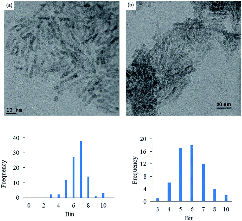 | ||
| Fig. 1 TEM of (a) TiO2-OA and (b) TiO2-10UCYPA. | ||
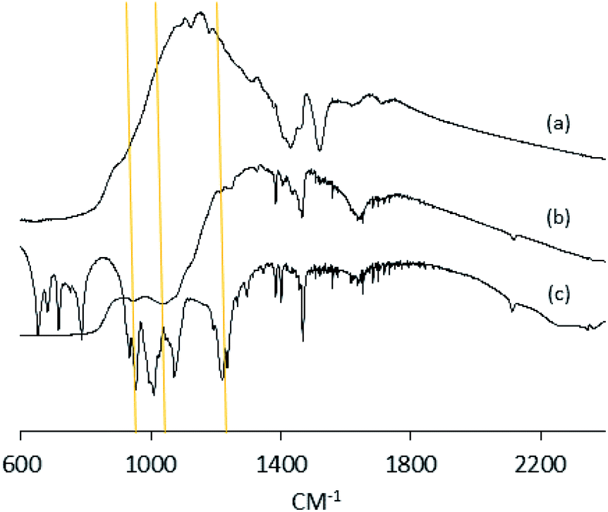 | ||
| Fig. 2 IR of (a) TiO2-OA, (b) TiO2-10UCYPA and (c) ligand 10UCYPA. | ||
The oleic acid on the surface of the TiO2 nanorods was partly replaced in ligand exchange reactions (LER) using 10-undecenylphosphinic acid (10UCYPA) as the reagent and new ligand (Scheme 1). The XRD patterns (Fig. 3) and TEM image of the ligand-exchanged titanium dioxide nanorods (TiO2-10UCYPA) are very similar to that of TiO2-OA nanorods, suggesting that the ligand exchange reaction carried out at 100 °C for 24 h has very little effect on the phase, size and shape and, hence, shape anisotropy, of the core of TiO2 nanorods, as could be expected.21 The two peaks at 1525 and 1430 cm−1 in the FTIR spectrum of TiO2-10UCYPA nanorods is very weak compared to that of the TiO2-OA nanorods, suggesting that most of oleic acid in TiO2-OA has been exchanged for the 10UCYPA ligand. The IR spectrum of 10UCYPA shows a P![[double bond, length as m-dash]](https://www.rsc.org/images/entities/char_e001.gif) O double bond valence vibration at 1220 cm−1 and a P–O–H absorption band at 950 m−1. However, these two bands are not present in the TiO2-10UCYPA nanorods. Also, a broad band, attributable to PO3 stretching, is observed at about 1051 cm−1 for the TiO2-10UCYPA nanorods. These data indicate that 10UCYPA is attached to the TiO2 surface through a tridentate bonding mode.12,25 The formation of tridentate phosphonate site P(OTi)3 in the TiO2-10UCYPA nanorods is confirmed by 31P NMR analysis as only one resonance at 29.6 ppm can be observed in the 31P NMR spectrum of TiO2-10UCYPA (Fig. 4).13,21,25
O double bond valence vibration at 1220 cm−1 and a P–O–H absorption band at 950 m−1. However, these two bands are not present in the TiO2-10UCYPA nanorods. Also, a broad band, attributable to PO3 stretching, is observed at about 1051 cm−1 for the TiO2-10UCYPA nanorods. These data indicate that 10UCYPA is attached to the TiO2 surface through a tridentate bonding mode.12,25 The formation of tridentate phosphonate site P(OTi)3 in the TiO2-10UCYPA nanorods is confirmed by 31P NMR analysis as only one resonance at 29.6 ppm can be observed in the 31P NMR spectrum of TiO2-10UCYPA (Fig. 4).13,21,25
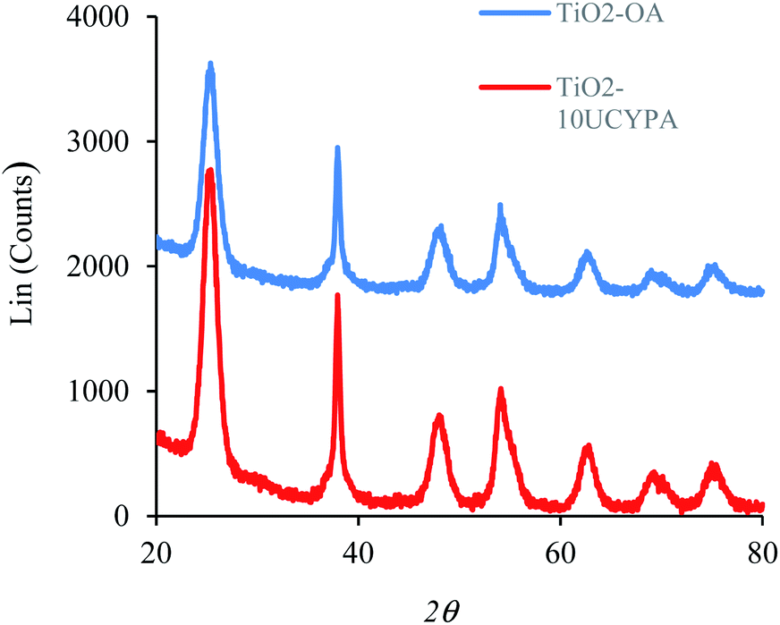 | ||
| Fig. 3 XRD patterns of TiO2-OA and ligand-exchanged product TiO2-10UCYPA. | ||
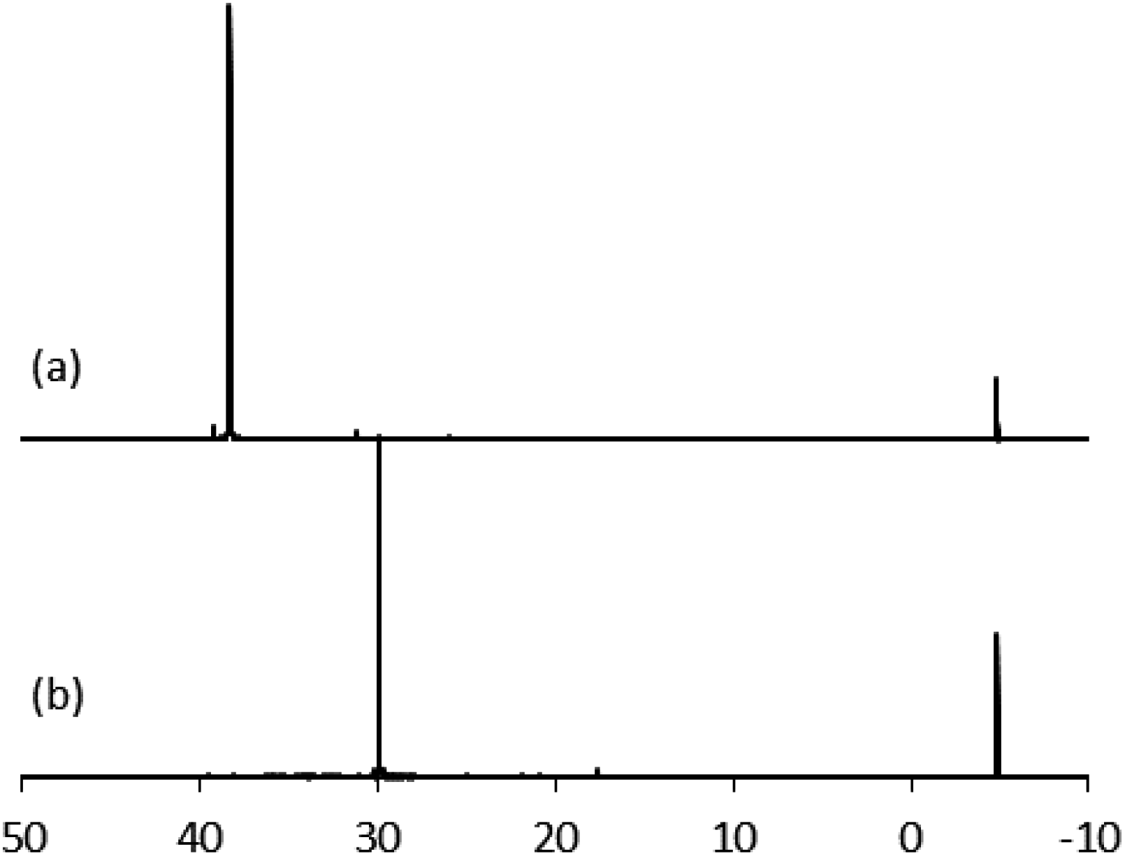 | ||
| Fig. 4 31P NMR of (a) 10UCYPA and (b) TiO2-10UCYPA in CDCl3. Triphenylphosphine gave a reference peak at −4.86 ppm. | ||
Chemical analysis (ICP and CHN) of the TiO2-OA and TiO2-10UCYPA nanorods (Table 1) indicates that 74.0% of oleic acid on the TiO2 nanorod surface has been replaced with 10UCYPA, which is consistent with the results from the FTIR analysis. This degree of ligand exchange is much higher than that (24.1%) observed using a much bulkier diethyl-6-[(7-oxycoumaryl)-undecenyl]phosphonate ligand under identical LER conditions.21 Therefore, the density of (alkynyl) photoreactive groups on the TiO2 surface is much higher for the TiO2-10UCYPA nanorods than that of the corresponding TiO2 nanorods with much bulkier photodimerisable coumarin groups.
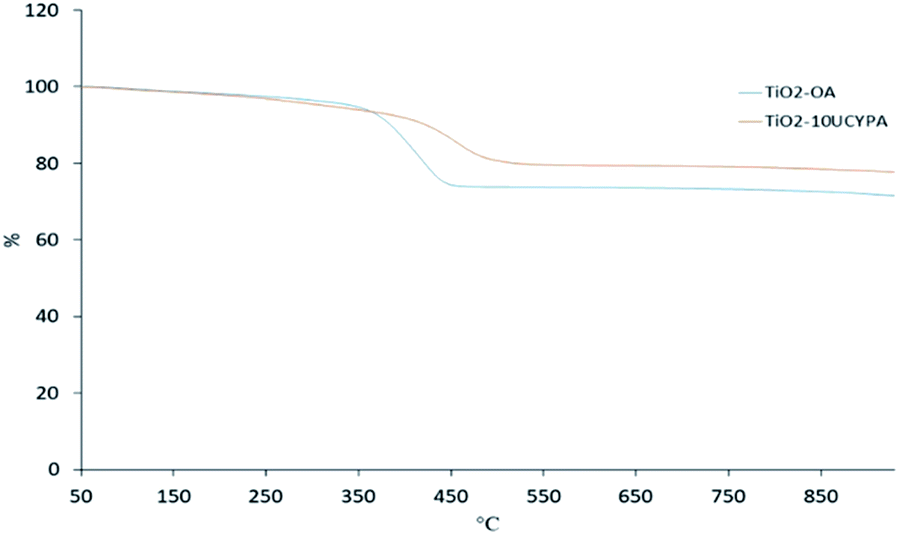
The TGA curves of the oleic acid stabilized titanium oxide TiO2-OA and 10UCYPA-exchanged product TiO2-10UCYPA are shown in Fig. 5. A major weight loss occurs in the temperature range of 350 °C to 450 °C due to thermal decomposition of the organic ligands for the TiO2-OA nanocomposites. The residue at 930 °C is 71.6%. As for TiO2-10UCYPA, the major weight loss has moved to 400 °C to 510 °C and residue at 930 °C is 77.7%. These data future support the FTIR, 31P NMR and chemical analyses above.
 | ||
| Fig. 5 TGA traces for the TiO2-OA and TiO2-10UCYPA inorganic/organic nanocomposites. | ||
The ligand-exchanged product TiO2-10UCYPA can be easily dissolved in chlorobenzene at high concentrations (40 wt%), which is much higher than that (20 wt%) observed for the corresponding TiO2 nanorods with photodimerisable coumarin groups prepared under identical conditions.21 Solutions of the TiO2-10UCYPA nanorods (20 wt%), suitable for deposition as a thin film on substrate surfaces, are stable for at least one month (Fig. 6).
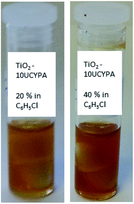 | ||
| Fig. 6 Images of the stable colloidal solutions of TiO2-10UCYPA inorganic/organic nanocomposites in chlorobenzene at two different concentrations (20 wt% and 40 wt%). | ||
Samples of the oleic acid-stabilized titanium dioxide nanorods (TiO2-OA) and the 10UCYPA-exchanged titanium dioxide nanorods (TiO2-10UCYPA) were dissolved in chlorobenzene to produce 20 wt% solutions in each case. The chlorobenzene solvent was then allowed to slowly evaporate at room temperature and the percentage concentration of the nanorods determined by changes in the weight of the residual solution. The images of these chlorobenzene/nanorod solutions using polarized optical microscopy (POM) at a concentration of 60 wt%, show the presence of coloured, birefringent domains (Fig. 7). Disclinations are observed at domain boundaries characteristic of the lyotropic liquid crystalline state and, in this case, of a nematic phase. These samples are fluid and disturbed by application of slight pressure, resulting in ‘flashing’ of the POM images, as typically observed in nematic phases. Further investigations are required to confirm the lyotropic liquid crystalline nature of these colloidal solutions. However, a nematic phase could facilitate domain formation of nanorods with their long axes in the substrate plane, due to the drying and spin coating process.21
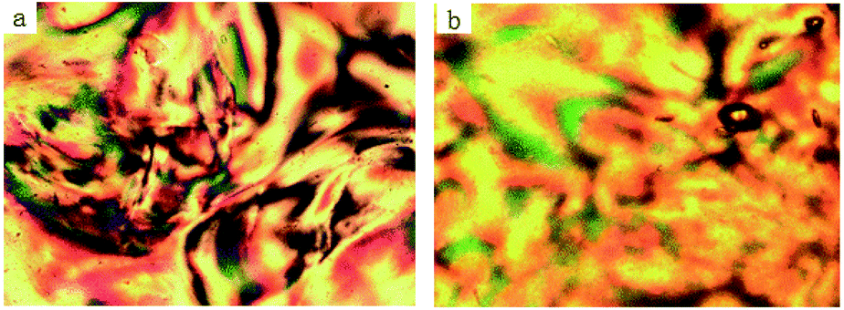 | ||
| Fig. 7 POM images of (a) TiO2-OA and (b) TiO2-10UCYPA inorganic/organic nanocomposites captured at concentration of 60% (wt/wt) in chlorobenzene. | ||
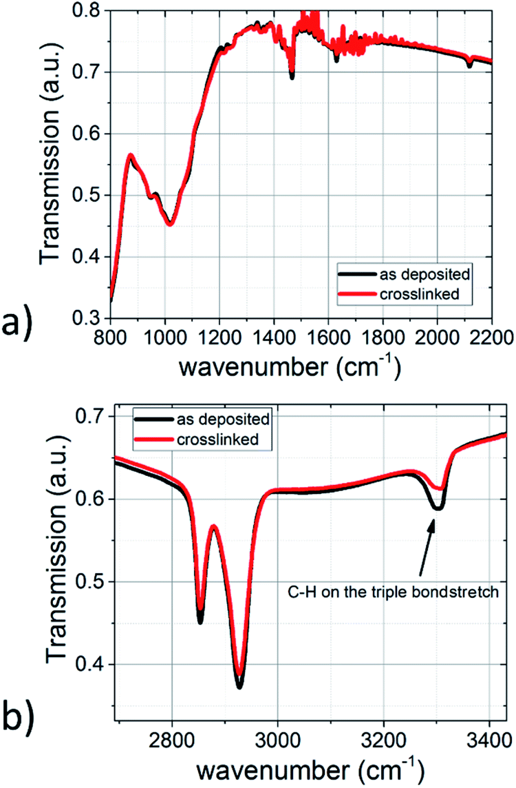
The IR spectra of the TiO2-10UCYPA films before and after polymerisation, shown in Fig. 8, reveal that the peak at 1050 cm−1, due to the phosphate group bonded with TiO2 surface, is not affected by the polymerisation reaction. However, the triple bond stretch at about 2150 cm−1 and acetylenic C–H stretch at about 3300 cm−1 are both much lower in intensity after polymerisation, suggesting that most of the TiO2-10UCYPA nanorods have been joined together by polymerisation of the alkyne functional groups.26,27 The polymer network films are insoluble in the chlorobenzene solvent used to prepare the initial solutions as shown in Table 2.
 | ||
| Fig. 8 FTIR spectra of the TiO2-10UCYPA thin films before and after UV crosslinking. | ||
| Sample | Film thickness before washing (nm) | Film thickness after washing (nm) |
|---|---|---|
| TiO2-10UCYPA | 210 ± 10 | 207 ± 7 |
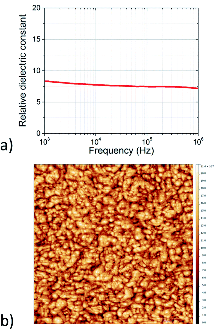
Thin films of the TiO2-10UCYPA nanorods were created by spin coating of the colloidal solutions as shown in Fig. 6 on pre-deposited electrodes. The dielectric constant of the films were extracted using a simple parallel RC model. The relative dielectric constant, k, was found to be 7–9 at frequencies between 1 kHz to 1 MHz, see Fig. 9a. The morphology of the films was studied with AFM, as shown in Fig. 9b, and is in line with the results obtained for TiO2-OA, with a RMS roughness of the order of 2–3 nm (ESI†).
 | ||
| Fig. 9 (a) Relative dielectric constant of the TiO2-10UCYPA thin films as extracted from impedance spectra. (b) AFM scan over a 1 μm × 1 μm region of a thin film of the TiO2-10UCYPA nanorods. | ||
In order to demonstrate the potential of this organic/inorganic hybrid dielectric material top-gate, bottom-contact thin-film transistors (TFTs) were fabricated using solution-processed ZnO as the channel material (Fig. 10a). In brief, 50 nm-thick Al source and drain electrodes were deposited onto glass substrates via thermal sublimation under high vacuum followed by the deposition (spin coating and annealing) of the ZnO channel layer in air. Device fabrication was completed with the deposition of the dielectric and the Al gate electrode. Electrical characterization was performed under inert atmosphere inside a nitrogen glovebox. The transfer (drain current ID versus gate voltage VG) and the output (drain current ID versus drain voltage VD) characteristic (Fig. 10b and c respectively) demonstrate clear n-channel transistor behaviour (electron accumulation under positive gate bias) with current on/off ratios of 104, turn-on voltage (VON) 1.2 V and a threshold voltage (VT) of 6.2 V (Fig. 10d). The electron mobility calculated from the square root of ID vs. VG in saturation is around 4.6 10−3 cm2 V−1 s−1. The results highlight the potential of TiO2-10UCYPA as a cross-linkable hybrid dielectric for TFTs. Further optimization in processing conditions is still needed to reduce both hysteresis and sub-threshold leakage.
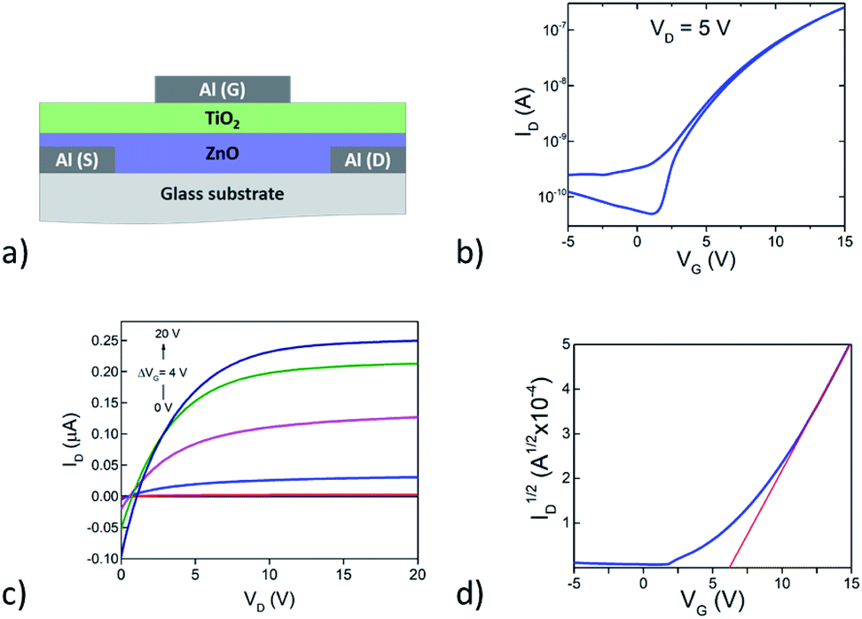 | ||
| Fig. 10 (a) Schematic of the TFT device with ZnO as the semiconductor and TiO2-10UCYPA as the dielectric layer. (b) Transfer characteristic ID–VG at a drain voltage of 5 V. (c) output characteristics ID–VD at gate voltages of 0 V, 4 V, 8 V, 12 V, 16 V and 20 V; a slight hysteresis of the curves is at the origin of the non-zero crossing of these output characteristics. (d) The threshold voltage was estimated by a linear fit of ID1/2 vs. VG is ≈6.2 V. | ||
Conclusions
Photopolymerisable anatase TiO2 nanorods (TiO2-10UCYPA) have been prepared by ligand exchange reactions (LER) from oleic acid capped TiO2 nanorods (TiO2-OA). Solutions of these nanorods in chlorobenzene were used to deposit uniform thin films of the TiO2-10UCYPA nanorods on an aluminium electrode on a glass substrate and then photopolymerised to form insoluble thin films with a moderately high dielectric constant, k = 7–9. Microscale test Thin Film Transistors (TFTs) fabricated using a zinc oxide channel semiconductor, also deposited from solution, a TiO2-10UCYPA nanorod dielectric layer and an aluminium gate electrode, show n-type transistor behaviour with current on/off ratios of 104, a turn-on voltage (VON) 1.2 V and a threshold voltage (VT) of 6.2 V.Conflicts of interest
There are no conflicts to declare.Acknowledgements
The research leading to these results received funding from the EPSRC under the grant agreement EP/J001597/1 and Researchers Supporting Project number (RSP-2020/160), King Saud University, Riyadh, Saudi Arabia. T. D. A. acknowledges the King Abdullah University of Science and Technology for financial support.Notes and references
- W. Hu, H. Li, J. B. Xu and L. Wang, ACS Appl. Mater. Interfaces, 2018, 10, 25878–25901 CrossRef PubMed.
- H. Yan, Z. Chen, Y. Zheng, C. Newman, J. R. Quinn, F. Dotz, M. Kastler and A. Facchetti, Nature, 2009, 457, 679–687 CrossRef CAS PubMed.
- R. Pelton, X. Geng and M. Brook, Adv. Colloid Interface Sci., 2006, 127, 43–53 CrossRef CAS PubMed.
- A. Wold, Chem. Mater., 1993, 5, 280–283 CrossRef CAS.
- L. A. Majewski, R. Schroeder and M. Grell, Adv. Funct. Mater., 2005, 15, 1017–1022 CrossRef CAS.
- P. D. Cozzoli, A. Kornowski and H. Weller, J. Am. Chem. Soc., 2003, 125, 14539–14548 CrossRef CAS PubMed.
- J. Joo, S. G. Kwon, T. Yu, M. Cho, J. Lee, J. Yoon and T. Hyeon, J. Phys. Chem. B, 2005, 109, 15297–15302 CrossRef CAS PubMed.
- Q. Qu, H. Geng, R. Peng, Q. Cui, X. Gu, F. Li and M. Wang, Langmuir, 2010, 26, 9539–9546 CrossRef CAS PubMed.
- N. Nakayama and T. Hayashi, Colloids Surf., A, 2008, 317, 543–550 CrossRef CAS.
- S. Mallakpour and R. Aalizadeh, Prog. Org. Coat., 2013, 76, 648–653 CrossRef CAS.
- R. Helmy and A. Y. Fadeev, Langmuir, 2002, 18, 8924–89248 CrossRef CAS.
- G. Guerrero, P. H. Mutin and A. Vioux, Chem. Mater., 2001, 13, 4367–4373 CrossRef CAS.
- A. Maliakal, H. Katz, M. Cotts Pat, S. Subramoney and M. Peter, J. Am. Chem. Soc., 2005, 127, 14655–14662 CrossRef CAS PubMed.
- M. P. Aldred, A. E. A. Contoret, S. R. Farrar, S. M. Kelly, D. Mathieson, M. O'Neill, W. C. Tsoi and P. A. Vlachos, Adv. Mater., 2005, 17, 1368–1372 CrossRef CAS.
- A. E. A. Contoret, S. R. Farrar, P. O. Jackson, S. M. Khan, L. May, M. O'Neill, J. E. Nicholls, S. M. Kelly and G. J. Richards, Adv. Mater., 2000, 12, 971–974 CrossRef CAS.
- C. D. Müller, A. Falcou, N. Reckefuss, M. Rojahn, V. Wiederhirn, P. Rudati, H. O. Frohne Nuyken, H. Becker and K. Meerholz, Nature, 2003, 421, 829–833 CrossRef PubMed.
- M. O'Neill and S. M. Kelly, Adv. Mater., 2003, 15, 1135–1146 CrossRef.
- M. O'Neill and S. M. Kelly, Adv. Mater., 2011, 23, 566–584 CrossRef PubMed.
- A. Liedtke, L. Chunhong, M. O'Neill, P. E. Dyer, S. P. Kitney and S. M. Kelly, ACS Nano, 2010, 4, 3248–3253 CrossRef CAS PubMed.
- I. McCulloch, W. Zhang, M. Heeney, C. Bailey, M. Giles, D. Graham, M. Shkunov, D. Sparrowe and S. Tierney, J. Mater. Chem., 2003, 13, 2436–2444 RSC.
- F. Cheng, E. Verrelli, F. A. Alharti, S. M. Kelly, M. O'Neill, N. Kemp, S. P. Kitney, K. T. Lai, G. H. Mehl and T. Anthopoulos, Nanoscale Adv., 2019, 1, 254–264 RSC.
- G. Caputo, R. Cingolani, P. D. Cozzoli and A. Athanassiou, Phys. Chem. Chem. Phys., 2009, 11, 3692–3700 RSC.
- R. Takahashi, S. Takenaka, S. Sato, T. Sodesawa, K. Ogura and K. Nakanishi, J. Chem. Soc., Faraday Trans., 1998, 94, 3161–3168 RSC.
- M. Nara, H. Torii and M. Tasumi, J. Phys. Chem., 1996, 100, 19812–19817 CrossRef CAS.
- J. Randon, P. Blanc and R. Paterson, J. Membr. Sci., 1995, 98, 119–129 CrossRef CAS.
- C. Sangregorio, E. Dalcanal and G. G. Condorelli, Nanoscale, 2013, 5, 1438–11446 Search PubMed.
- G. Socrates, Infrared and Raman Characteristic Group Frequencies, Tables and Charts, John Wiley & Sons, New York, 3rd edn, 2004 Search PubMed.
Footnote |
| † Electronic supplementary information (ESI) available: Figures: leakage current and relative dielectric constant through a 188 nm TiO2-10UCYPA thin film measured in air and an AFM scan for a TiO2-OA thin film. See DOI: 10.1039/d0ra04445h |
| This journal is © The Royal Society of Chemistry 2020 |