
 Open Access Article
 This Open Access Article is licensed under a Creative Commons Attribution-Non Commercial 3.0 Unported Licence
Enhancing the performance of blue quantum-dot light-emitting diodes through the incorporation of polyethylene glycol to passivate ZnO as an electron transport layer†
Jun-hao Suna,
Jia-hui Huanga,
Xu-yan Lan a,
Feng-chun Zhanga,
Ling-zhi Zhaoabc and
Yong Zhang*ab
a,
Feng-chun Zhanga,
Ling-zhi Zhaoabc and
Yong Zhang*ab
aInstitute of Semiconductor Science and Technology, South China Normal University, Guangzhou, 510631, China. E-mail: zycq@scnu.edu.cn
bGuangdong Engineering Technology Research Center of Low Carbon and Advanced Energy Materials, Guangzhou, 510631, China
cSCNU Qingyuan Institute of Science and Technology Innovation Co., Ltd., Qingyuan 511517, China
First published on 17th June 2020
Abstract
The balance between charge transport and charge injection is always a key factor in enhancing the performance of quantum-dot light-emitting diodes (QD-LEDs), particularly for the blue QDs due to their large optical band gap and relatively low valence band level compared with their green and red counterparts. High performance blue QD-LEDs have been demonstrated by blending polyethylene glycol (PEG) into solution-processed ZnO nanocrystals as the electron transport layer. PEG can effectively tune the electron mobility of ZnO and simultaneously passivate its surface defect states. As a result, the maximum current efficiency (CE) and external quantum efficiency (EQE) of the blue QD-LEDs increased from 4.33 cd A−1 and 9.98% for pure ZnO to 8.03 cd A−1 and 14.84% for 4% PEG blended into ZnO, respectively. Furthermore, operational lifetime of the device is also significantly improved from 8.95 h to 25.06 h. This result indicates that PEG is a promising material for regulating the charge balance of the blue QD-LEDs.
Introduction
Colloidal quantum dots (QDs) have been widely used as luminescent materials in light-emitting devices due to their excellent optical property.1,2 Quantum dot light-emitting diodes (QD-LEDs) exhibit a high luminescence quantum yield, narrow emission with a small full width at half maximum (FWHM), size-adjustable spectrum, superior thermal stability and simple solution process, all of which make it a promising application for the next generation lighting source and display technology.3,4 The polymers, organic small molecules, and inorganic metal oxides are used as hole transport layers (HTLs) of QD-LEDs.5–7 The metal oxides like ZnO or TiO2, have been widely adopted towards electron transport layers (ETLs) because of their matched energy levels and excellent electron transport properties.8,9 However, holes are more difficult to inject into the QD emissive layer than electrons because most QDs have a much lower valence band than the highest occupied molecular orbital (HOMO) level of HTL.7,10 To enhance the QD-LED performance, researchers focus on the balanced injection of the electrons and holes in the devices and the reducing QDs charged by optimizing the QD nanostructure, device architecture, and interfacial modification.11–18QD-LEDs based on ZnO nanoparticles (NPs) as ETL and organic/polymer films as HTLs have been one of the most popular device structures.9,14 Solution-processed ZnO NPs have high electron mobility of 10−3 cm2 V−1 s−1,19 which is higher than that of the commonly used organic HTL materials and will lead to unbalanced carrier transport in the QD-LEDs. In additional, ZnO NPs have a lot of defects, such as surface groups and surface defect states within the band gap of ZnO associated with the oxygen vacancies, zinc vacancies, zinc interstitials and oxygen interstitials,20,21 resulting in the QD exciton quenching of the QD/ZnO interface. Therefore, the introduction of additional functional layers between the ZnO ETL and the QD emissive layer or doping of the ZnO layer are used to optimize the charge-transport balance and the interface fluorescence quenching of the ZnO-based QD-LEDs.14,22–26 Compared with their red and green counterparts, the blue QD-LEDs exhibit a larger hole injection potential barrier due to their large optical band gap and relatively low valence band level, which leads to the imbalance between the electron–hole injection and restrict the development of QD-LEDs in display applications.27,28 Recently, Sun et al. used polyvinylpyrrolidone-doped ZnO NPs to reduce the electron injection and realized a maximum EQE of 2.95% for the blue QD-LEDs.29 Wang et al., reported metal complex-doped AZO NPs and organic molecule-doped poly(9,9-dioctylfluorene-co-N-(4-(3-methylpropyl))diphenylamine) as ETL and HTL of the blue QD-LEDs, respectively, and achieved maximum external quantum efficiency (EQE) of 10.7%.30 Wang et al. tuned the electron transport properties of ZnO NPs by optimizing the synthesis procedure and demonstrated a peak EQE of 19.8% for the blue QD-LEDs.31 In spite of these improvements, the performance of blue QD-LEDs is still much below than those of the red and green QD-LEDs.32
Polyethylene glycol (PEG), a neutral surfactant, is widely used as an additive to improve the performance of polymer light-emitting diodes (PLEDs)33,34 and perovskite light-emitting diodes (PeLEDs).35 Herein, we successfully realized high performance blue QD-LEDs by blending PEG with the ZnO NPs to form PEG:ZnO composite films as ETLs. Based on this method, the maximum current efficiency (CE) and EQE of the blue QD-LEDs reached 8.03 cd A−1 and 14.84%, respectively, for the optimized PEG blend ratio of 4%. Compared with the pure ZnO NP ETL, the electron mobility of the PEG:ZnO NP composite film was obviously reduced. Simultaneously, PEG can passivate the surface defect states of ZnO NPs due to the interaction between PEG and ZnO NPs, resulting in decreased QD exciton quenching of the QD/ZnO interface.
Experimental section
1. Preparation of materials
ZnO NPs were synthesized via a low-temperature solution-precipitation method reported by Kwak et al.4 Poly(3,4-ethylenedioxythiophene)/poly(styrenesulfonate) (PEDOT:PSS), poly(9-vinlycarbazole) (PVK) and polyethylene glycol (PEG, Mn = 1500) were purchased from Sigma-Aldrich. Blue QDs (ZnCdS/ZnS/oleic acid core/shell-type) were obtained from Guangdong Poly Opto Electronics Co., Ltd. All the materials were used as received without further purification.2. Preparation of devices
In this study, blue QD-LEDs have the structure of glass/ITO/PEDOT:PSS/PVK/QDs/ZnO or ZnO:PEG/Al. The ITO glass substrates with a sheet resistance of 15 Ω per square were ultrasonically cleaned with a detergent, deionized water, acetone, and isopropyl alcohol, sequentially for 15 min. PEDOT:PSS were spin-coated on the pre-cleaned and O2-plasma-treated ITO substrates at 2000 rpm for 60 s and then heated on a hot plate at 150 °C for 20 min to remove the residual water. All the samples were then transferred into a nitrogen-filled glove box for depositing subsequent multilayer films and fabricating cathodes. PVK (in chlorobenzene, 8 mg mL−1) and the blue QDs (in octane, 10 mg mL−1) were sequentially spin-coated on top of the PEDOT:PSS film at 2000 rpm for 60 s as the HTL and emissive layer, respectively. The HTL and QD layers were heated at 120 °C for 30 min and 100 °C for 20 min, respectively, before spin-coating the next layer. The ZnO NPs and PEG were dissolved separately in ethanol and then blended at different ratios to achieve the appropriate weight ratio. The blended solutions of ZnO and PEG were deposited on the top of the QD emissive layer at 2000 rpm for 60 s and then baked at 100 °C for 30 min. Finally, the samples were transferred into a thermal evaporation system, and the Al cathodes (100 nm) were evaporated on the top of PEG:ZnO composite films under a vacuum of 4 × 10⁻⁴ Pa.3. Characterization
The measurement of the device properties was carried out in a nitrogen-filled glove-box at room temperature. A Keithley 2400 voltage and current source meter and a Konica Minolta LS-150 luminance meter were used for current–voltage and light output measurements, respectively. The electroluminescence (EL) spectra of the corresponding QD-LEDs were collected by an Ocean Optics fiber optical spectrometer (Maya2000 Pro). The PL spectra of the glass/PVK/QD/ZnO or ZnO:PEG films were measured using a Horiba FluoroMax-4 spectrofluorometer. Transient PL measurements were performed on a lifetime spectrometer (FL920, Edinburgh Instrument) at room temperature, and the samples were excited by a 375 nm pulsed diode laser. A function wavelength generator (Rigol DG4162) was used to provide pulse voltages for the transient EL tests. AFM images of the films were recorded with NT-MDT. XPS and UPS measurements were carried on an ESCALAB 250Xi (Thermo) system. Samples for the XPS and UPS measurements were excited with an Al Kα (1486.6 eV) X-ray source and He I (21.22 eV) ultraviolet source, respectively. The transmission electron microscopy (TEM) images of the ZnO and PEG:ZnO NPs were obtained using JEM-2100HR operated at an accelerating voltage from 100–400 kV. The UV-visible absorbance spectrum of the ZnO NP thin film was recorded using a HP8453A spectrophotometer.Results and discussion
The device structure of the blue QD-LED and the energy level diagram of the used materials are illustrated in Fig. 1a and b, respectively. The HOMO and LUMO, conduction and valence band levels of the materials are taken from the corresponding reports.14,36 The UPS measurement was used to obtain the valence band maximum (VBM) and conduction band minimum (CBM) of the ZnO NPs. Fig. 1c shows the UPS spectrum of the ZnO NP thin films. The Eonset (Fermi edges) and Ecutoff (secondary electron edges) are determined by the intercepts of the tangents to the peaks with the extrapolated baselines. According to EVBM = EHe − (Ecutoff − Eonset),19 where EHe is the energy of ultraviolet source He I (21.22 eV), VBM level of the ZnO NPs is 7.22 eV. Based on the VBM and the optical band-gap of the ZnO NPs (3.42 eV) derived from the absorbance spectrum (Fig. 1d, CBM level of the ZnO film is calculated to be 3.80 eV. The thicknesses of the PEDOT:PSS, PVK, QDs, and PEG:ZnO are 40 nm, 20 nm, 20 nm, and 40 nm, respectively. The ZnO NP ETL and PVK HTL have been widely used in the QD-LEDs. The electron mobility of the ZnO NPs (∼10−3 cm2 V−1 s−1) is much larger than the hole mobility of PVK (∼10−6 cm2 V−1 s−1).14,15 As a result, the electron transport in the current device is more efficient than the hole transport. Moreover, the electron injection into the blue QDs through ZnO NP ETL is easier than the hole injection due to relatively larger energy barrier between the HOMO of PVK and the VBM of QDs. These factors can lead to excess electrons in the QD emissive layer. Therefore, we introduce a neutral surfactant PEG, blended with ZnO NPs, to regulate the electron mobility of ETL and improve the balance of the charge carriers.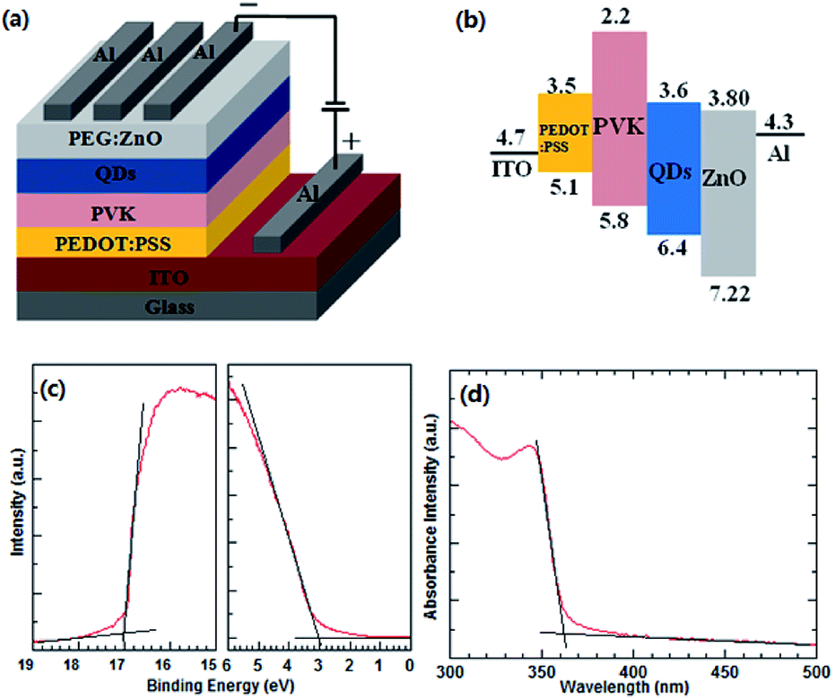 | ||
| Fig. 1 (a) Device structure of blue QD-LED and (b) energy level diagram of the used materials. UPS (c) and UV-visible (d) spectra of the ZnO NP thin film. | ||
Fig. 2a shows the current density and luminance versus the voltage (J–V–L) characteristics of the blue QD-LEDs with different PEG blend ratios as ETLs. It is clearly observed that proper blending of PEG into ZnO NPs as ETL can effectively enhance the QD-LED performance. The blue QD-LED with PEG(2%):ZnO as ETL shows a high current density than pure ZnO, but then the current density gradually decreases as the PEG blend concentration increases. For instance, at a driving voltage of 6 V, the current density increases from 272 mA cm−2 for pure ZnO to 303 mA cm−2 for PEG(2%):ZnO and then goes down to 261 mA cm−2 for PEG(4%):ZnO and 208 mA cm−2 for PEG(8%):ZnO. The PEG blended into ZnO NPs as ETL can facilitate the electron injection due to the interfacial interaction between the PEG and Al cathode.33 Fig. S1(a) and (b)† shows the UPS and UV-visible spectra of the PEG(4%):ZnO film. It can be seen that the VBM and CBM of ZnO reduced from 7.22 eV and 3.80 eV to 7.14 eV and 3.72 eV after 4% PEG blended into ZnO NPs, respectively. The reduction of CBM will facilitate the electrons to inject into the QD emissive layer. However, due to its electric insulating property, the PEG blend will lead to the decrease in the electron mobility of the ZnO NP ETL, resulting in the reduction in the current density at a blend ratio of more than 2%. The luminance intensity of the blue QD-LEDs reduces with the increase in the PEG blend concentration. However, the devices with the PEG blend demonstrate higher luminance intensity than the pure ZnO. The turn-on voltage reduces from 3.30 V for pure ZnO to 3.20 V for 2% PEG and then rises with increase in the PEG content. The corresponding device performances are listed in Table 1. The CE and EQE versus luminance properties of the corresponding QD-LEDs are presented in Fig. 2b. It can be found that the optimized PEG content is 4%. The maximum CE and EQE of QD-LED increase from 4.33 cd A−1 and 9.98% for pure ZnO to 8.03 cd A−1 and 14.84% for 4% PEG, respectively. No significant changes for the EL spectra of blue QD-LEDs are observed for the different PEG blend ratios at 30 mA cm−2 (as shown in Fig. 2c). The peak wavelength of these devices is located at about 465 nm, indicating that the PEG blend will not change the exciton recombination zone.
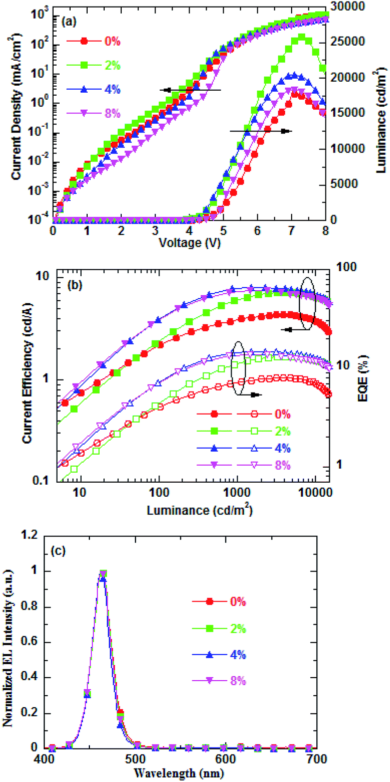 | ||
| Fig. 2 (a) Current density–voltage–brightness characteristics, (b) CE–luminance–EQE characteristics, and (c) normalized EL spectra of blue QD-LEDs for different PEG blend ratios. | ||
| PEG:ZnO | Von (V) | CE (cd A−1) | EQE (%) | μe (cm2 (V−1 s−1)) | ||
|---|---|---|---|---|---|---|
| @1000 cd m−2 | LEmax | @1000 cd m−2 | EQEmax | |||
| x = 0% | 3.30 | 3.84 | 4.33 | 7.08 | 9.98 | 3.21 × 10⁻⁴ |
| x = 2% | 3.20 | 5.93 | 7.14 | 10.94 | 13.18 | 7.26 × 10⁻⁵ |
| x = 4% | 3.50 | 7.85 | 8.03 | 14.49 | 14.84 | 4.73 × 10⁻⁵ |
| x = 8% | 3.84 | 7.16 | 7.41 | 13.23 | 13.68 | 7.30 × 10⁻⁶ |
For the same anode side, the improvement in the device performance of the blue QD-LEDs should be attributed to the PEG:ZnO composite as ETL. The electron-only devices of the different PEG blend ratios were fabricated to study the electron mobility. Fig. 3 shows the current density–voltage characteristics of the electron-only device with the device structure of glass/ITO/Al/PEG:ZnO (200 nm)/Al. It can be seen from Fig. 3 that the electron current density reduces as the PEG content increases, which indicates that the PEG matrix efficiently blocks the excess electron injection into the QD active layer and balances the electron and hole injection in QD-LEDs. The electron mobility of the PEG:ZnO composite films can be obtained by fitting the space-charge-limited-current region with the Child's law14 and are summarized in Table 1. As a result, the electron mobility of the ZnO film reduces from 3.21 × 10⁻⁴ cm2 V−1 s−1 to 7.26 × 10⁻⁵ cm2 V−1 s−1 for 2% PEG, 4.73 × 10⁻⁵ cm2 V−1 s−1 for 4% PEG, and 7.30 × 10⁻⁶ cm2 V−1 s−1 for 8% PEG. Obviously, the PEG blend can significantly regulate electron mobility of the ZnO NPs. This can be attributed to the insulating PEG material filling the inter domain sites between the ZnO NPs and alleviating the electron transport through the domain boundaries.37 We further applied AFM to characterize the film morphology of ZnO and PEG(4%):ZnO by spin-coating on the top of the glass/ITO/PEDOT:PSS/PVK/QDs (Fig. 4a and b). The film roughness shows slight increase from a root mean square (RMS) roughness of 1.9 nm to 2.4 nm after the PEG blending into the ZnO NPs. However, both the films show a smooth surface without voids or cracks.
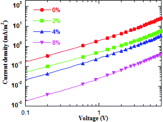 | ||
| Fig. 3 Current density and voltage curves for the electron-only devices with the different PEG blend ratios. | ||
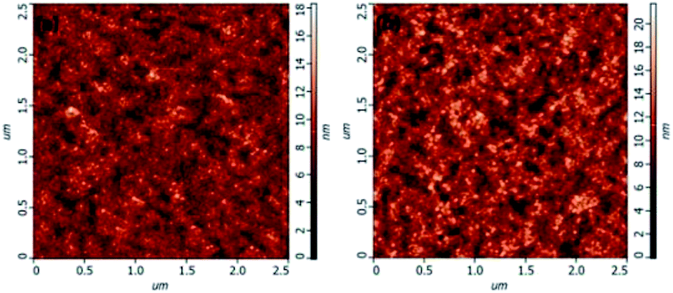 | ||
| Fig. 4 AFM images of ZnO (a) and PEG(4%):ZnO (b) films. | ||
To investigate the effects of the PEG blend on the surface defect of ZnO NPs, the surface elements of the ZnO and PEG(4%):ZnO layers were analyzed by the XPS measurements, as shown in Fig. 5a–c. The Zn 2p spectra in Fig. 5a display an energy difference of 23 eV between the two peaks, indicating that they both have a normal chemical state of Zn2+ for the compounds. However, there is 0.35 eV shift towards the higher binding energy for the ZnO:PEG film, suggesting more Zn atoms are bounded with a more stable chemical state. In Fig. 5b and c, the O 1s spectra can be deconvoluted into three peaks: OM 529.5, OV 530.9, and OOH 531.9 eV, where the OM, OV and OOH represent the metal–oxygen bond, oxygen vacancy, and hydrogen–oxygen group absorbed on the surface of the ZnO NPs, respectively.38 The oxygen vacancies significantly reduce from 32.79% to 22.54% after the PEG blending, while the hydrogen–oxygen groups increase from 8.10% to 20.59%. Herein, the reduced OV and increased OOH peaks suggest that the oxygen atoms of the PEG backbone tend to absorb onto the surface of the ZnO NPs.39 As shown in Fig. S2 and S3,† the TEM images reveal that the average particle size of the ZnO NPs increase from 5.06 to 5.59 nm after PEG blending, which further indicates that PEG is absorbed on the surface of the ZnO NPs. The PL spectra of ZnO and PEG(4%):ZnO in Fig. S4† show a wide trap-state emission from 450 nm to 650 nm. However, the PL peak intensity of the ZnO NPs reduces after the PEG blending, so it is inferred that the PEG blending can diminish the trap states of ZnO NPs. As a result, the oxygen atoms interact with the surface defects and fill the shallow traps near the conduction band edge, thus passivating the surface defect sites. The oxygen vacancy reduction will further lead to the reduction of the electron mobility in the ZnO NP, which is in good accordance with the reducing current density of the ZnO NP-based QD-LEDs with the increasing the PEG blend ratio.
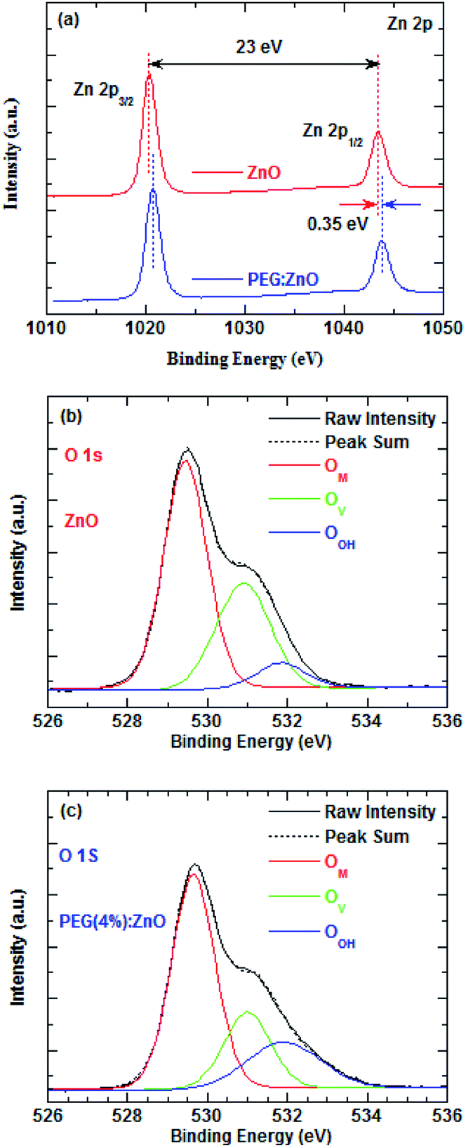 | ||
| Fig. 5 The XPS spectra of Zn 2p of ZnO and ZnO:PEG (a), O 1s of ZnO (b) and PEG:ZnO (c). | ||
Reduction of the ZnO traps can lower the possibility of trap-assisted recombination in the QDs/ZnO ETL interface. The interfacial charge accumulation and traps can significantly influence the photoluminescence and electroluminescence process by nonradiative recombination or exciton dissociation, thus decreasing the exciton lifetime. The PEG blend can effectively reduce the interface defects between the QD active layer and ZnO ETL, thus improving the QD exciton lifetime. The PL intensity of the blue QDs on the ZnO NP film of different PEG blend ratios were measured to evaluate the fluorescence quenching extent at the QD/ZnO ETL interface and are shown in Fig. 6a. The PL intensity of blue QDs increases as the PEG content increases and reduces above 4% PEG concentration. The PL intensity of the blue QDs increases by ∼240% after 4% PEG blended into the ZnO NPs.
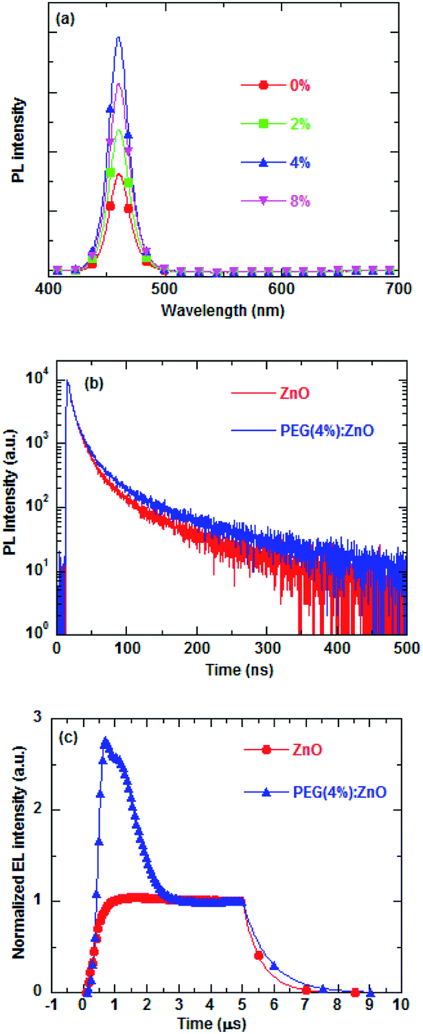 | ||
| Fig. 6 (a) PL intensities for glass/PVK/QDs/PEG(x%):ZnO with different PEG blend ratios, (b) time-resolved PL decay of glass/ITO/PEDOT:PSS/PVK/QD/ZnO or PEG(4%):ZnO/Al, and (c) transient EL of the corresponding blue QD-LEDs with ZnO and PEG(4%):ZnO as ETLs at the current density of 50 mA cm−2. | ||
The time-resolved photoluminescence (TRPL) and transient EL were carried out to study the effects of PEG blending on the exciton recombination (Fig. 6b and c). Fig. 6b shows the PL intensity of glass/ITO/PEDOT:PSS/PVK/QD/ZnO or PEG(4%):ZnO as a function of time. The TRPL decay curves can be fitted with a bi-exponential function. The average PL lifetime of the QDs increases from 29.05 ns to 36.33 ns after 4% PEG blend into the ZnO NPs, indicating that the PEG blend can restrain the fluorescence quenching of the QD/ZnO NP interface due to passivation of the surface defect of the ZnO NPs. The transient EL characteristics of the corresponding QD-LEDs are drawn in Fig. 6c. The luminance decay time of QD-LED increases from 560 ns to 830 ns after 4% PEG blended into the ZnO NPs as ETL. In addition, the turn-on overshoot luminance is observed in the transient EL of the PEG(4%):ZnO device, which is related to the radiative and nonradiative recombination of the injected charges.15,40 Based on the above discussion, the PEG blend induced passivation of the surface defect of ZnO NPs will effectively reduce the nonradiative recombination at the QD/ZnO interface. Therefore, the longer decay and strong turn-on overshoot luminance in the transient EL of the QD-LED having PEG blend into the ZnO NPs is due to the diminishing nonradiative recombination in QD-LED.
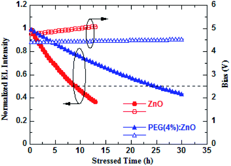
The PEG-induced surface passivation of the ZnO NPs will have an important effect on the device operational stability. Fig. 7 shows the change in the normalized brightness of the QD-LEDs based on ZnO and PEG(4%):ZnO as ETL with operation time at the same initial luminance of 1000 cd m−2 with a constant current driving. The blue QD-LED displays a slow luminance decay characteristic after PEG was blended into the ZnO NPs as ETL. The reducing electron mobility and surface defects of the ZnO NPs will obviously diminished the QD charging and exciton quenching in the ETL/QD interface, thus enhancing the stability of the device. The half-life-time of blue QD-LED increases from 8.95 h for the pure ZnO to 25.06 h for PEG(4%):ZnO. The improving device stability should be attributed to the more balanced electron and hole injection due to the PEG blend-induced defect passivation and electron mobility reduction of the ZnO NPs. Meanwhile, the driving voltage of the PEG(4%):ZnO-based QD-LED is also more stable than the pure ZnO (as shown in Fig. 7), showing a rise of 0.09 V after 25.06 h operation, while that of the pure ZnO-based device showed a rise of 0.24 V after 8.95 h.
 | ||
| Fig. 7 Brightness and driving voltage versus the operation time characteristics of QD-LEDs using ZnO and PEG(4%):ZnO as ETLs. | ||
Conclusions
In summary, we introduced PEG blended with ZnO NPs as ETL to regulate the charge balance of the blue QD-LEDs by adjusting the blend ratio of PEG. The introduction of PEG can efficiently passivate the ZnO NP surface defect and reduce the electron mobility of ZnO ETL, leading to an improved charge balance and fluorescence quenching of the QD/ETL interface for the blue QD-LEDs. As a result, the maximum current efficiency and EQE reached 8.03 cd A−1 and 14.84%, respectively, which is an increase in about 50% than that of the device without PEG blend. This result demonstrates that PEG is a promising material for adjusting the charge balance of the blue QD-LEDs.Conflicts of interest
There are no conflicts of interest to declare.Acknowledgements
This work was supported by the Nature Science Foundation of China (61377065 and 61574064), the Science and Technology Planning Project of Guangdong Province (2015B010132009 and 2019B090905005), and the Nature Science Foundation of Guangdong Province (2020A1515010786).Notes and references
- W. Nan, Y. Niu, H. Qin, F. Cui, Y. Yang, R. Lai, W. Lin and X. Peng, J. Am. Chem. Soc., 2012, 134, 19685–19693 CrossRef CAS PubMed.
- E. Jang, S. Jun, H. Jang, J. Lim, B. Kim and Y. Kim, Adv. Mater., 2010, 22, 3076–3080 CrossRef CAS PubMed.
- X. Dai, Y. Deng, X. Peng and Y. Jin, Adv. Mater., 2017, 29, 1607022 CrossRef PubMed.
- J. Kwak, W. K. Bae, D. Lee, I. Park, J. Lim, M. Park, H. Cho, H. Woo, D. Y. Yoon, K. Char, S. Lee and C. Lee, Nano Lett., 2012, 12, 2362–2366 CrossRef CAS PubMed.
- J. Zhao, J. A. Bardecker, A. M. Munro, M. S. Liu, Y. Niu, I. K. Ding, J. Luo, B. Chen, A. K. Y. Jen and D. S. Ginger, Nano Lett., 2006, 6, 463–467 CrossRef CAS PubMed.
- P. O. Anikeeva, J. E. Halpert, M. G. Bawendi and V. Bulović, Nano Lett., 2007, 7, 2196–2200 CrossRef CAS PubMed.
- L. Qian, Y. Zheng, J. Xue and P. H. Holloway, Nat. Photonics, 2011, 5, 543 CrossRef CAS.
- K. Qasim, J. Chen, Z. Li, W. Lei and J. Xia, RSC Adv., 2013, 3, 12104–12108 RSC.
- Y. Shirasaki, G. J. Supran, M. G. Bawendi and V. Bulović, Nat. Photonics, 2012, 7, 13 CrossRef.
- Y. L. Shi, F. Liang, Y. Hu, X. D. Wang, Z. K. Wang and L. S. Liao, J. Mater. Chem. C, 2017, 5, 5372–5377 RSC.
- J. Lim, B. G. Jeong, M. Park, J. K. Kim, J. M. Pietryga, Y. S. Park, V. I. Klimov, C. Lee, D. C. Lee and W. K. Bae, Adv. Mater., 2014, 26, 8034–8040 CrossRef CAS PubMed.
- Y. Yang, Y. Zheng, W. Cao, A. Titov, J. Hyvonen, J. R. Manders, J. Xue, P. H. Holloway and L. Qian, Nat. Photonics, 2015, 9, 259–266 CrossRef CAS.
- H. Shen, Q. Gao, Y. Zhang, Y. Lin, Q. Lin, Z. Li, L. Chen, Z. Zeng, X. Li, Y. Jia, S. Wang, Z. Du, L. S. Li and Z. Zhang, Nat. Photonics, 2019, 13, 192–197 CrossRef CAS.
- X. Dai, Z. Zhang, Y. Jin, Y. Niu, H. Cao, X. Liang, L. Chen, J. Wang and X. Peng, Nature, 2014, 515, 96 CrossRef CAS PubMed.
- M. D. Ho, D. Kim, N. Kim, S. M. Cho and H. Chae, ACS Appl. Mater. Interfaces, 2013, 5, 12369–12374 CrossRef CAS PubMed.
- J. Pan, J. Chen, Q. Huang, L. Wang and W. Lei, RSC Adv., 2017, 7, 43366–43372 RSC.
- J. Li, Z. Liang, Q. Su, H. Jin, K. Wang, G. Xu and X. Xu, ACS Appl. Mater. Interfaces, 2018, 10, 3865–3873 CrossRef CAS PubMed.
- Y. Liu, C. Jiang, C. Song, J. Wang, L. Mu, Z. He, Z. Zhong, Y. Cun, C. Mai, J. Wang, J. Peng and Y. Cao, ACS Nano, 2018, 12, 1564–1570 CrossRef CAS PubMed.
- J. Pan, J. Chen, Q. Huang, Q. Khan, X. Liu, Z. Tao, Z. Zhang, W. Lei and A. Nathan, ACS Photonics, 2016, 3, 215–222 CrossRef CAS.
- H. Yadav, K. Sreenivas, V. Gupta, S. Singh and R. Katiyar, J. Mater. Res., 2007, 22, 2404–2409 CrossRef CAS.
- L. Schmidt-Mende and J. L. MacManus-Driscoll, Mater. Today, 2007, 10, 40–48 CrossRef CAS.
- K. Ding, H. Chen, L. Fan, B. Wang, Z. Huang, S. Zhuang, B. Hu and L. Wang, ACS Appl. Mater. Interfaces, 2017, 9, 20231–20238 CrossRef CAS PubMed.
- A. Castan, H.-M. Kim and J. Jang, ACS Appl. Mater. Interfaces, 2014, 6, 2508–2515 CrossRef CAS PubMed.
- S. Cao, J. Zheng, J. Zhao, Z. Yang, C. Li, X. Guan, W. Yang, M. Shang and T. Wu, ACS Appl. Mater. Interfaces, 2017, 9, 15605–15614 CrossRef CAS PubMed.
- M. Yan, Y. Li, Y. Zhou, L. Liu, Y. Zhang, B. You and Y. Li, IEEE Photonics J., 2017, 9, 1–8 Search PubMed.
- J. Pan, C. Wei, L. Wang, J. Zhuang, Q. Huang, W. Su, Z. Cui, A. Nathan, W. Lei and J. Chen, Nanoscale, 2018, 10, 592–602 RSC.
- X. Qu, N. Zhang, R. Cai, B. Kang, S. Chen, B. Xu, K. Wang and X. W. Sun, Appl. Phys. Lett., 2019, 114, 071101 CrossRef.
- O. Wang, L. Wang, Z. Li, Q. Xu, Q. Lin, H. Wang, Z. Du, H. Shen and L. S. Li, Nanoscale, 2018, 10, 5650–5657 RSC.
- K. Sun, F. Li, Q. Zeng, H. Hu and T. Guo, Org. Electron., 2018, 63, 65–70 CrossRef CAS.
- F. Wang, W. Sun, P. Liu, Z. Wang, J. Zhang, J. Wei, Y. Li, T. Hayat, A. Alsaedi and Z. a. Tan, J. Phys. Chem. Lett., 2019, 10, 960–965 CrossRef CAS PubMed.
- L. Wang, J. Lin, Y. Hu, X. Guo, Y. Lv, Z. Tang, J. Zhao, Y. Fan, N. Zhang, Y. Wang and X. Liu, ACS Appl. Mater. Interfaces, 2017, 9, 38755–38760 CrossRef CAS PubMed.
- H. Shen, Q. Lin, W. Cao, C. Yang, N. T. Shewmon, H. Wang, J. Niu, L. S. Li and J. Xue, Nanoscale, 2017, 9, 13583–13591 RSC.
- X. Y. Deng, W. Lau, K. Y. Wong, K. Low, H. F. Chow and Y. Cao, Appl. Phys. Lett., 2004, 84, 3522–3524 CrossRef CAS.
- L. Nouzman and G. L. Frey, J. Mater. Chem. C, 2017, 5, 12744–12751 RSC.
- L. Song, X. Guo, Y. Hu, Y. Lv, J. Lin, Z. Liu, Y. Fan and X. Liu, J. Phys. Chem. Lett., 2017, 8, 4148–4154 CrossRef CAS PubMed.
- T. Cheng, Z. Wang, S. Jin, F. Wang, Y. Bai, H. Feng, B. You, Y. Li, T. Hayat and Z. A. Tan, Adv. Opt. Mater., 2017, 5, 1700035 CrossRef.
- S. B. Jo, J. H. Lee, M. Sim, M. Kim, J. H. Park, Y. S. Choi, Y. Kim, S.-G. Ihn and K. Cho, Adv. Energy Mater., 2011, 1, 690–698 CrossRef CAS.
- V. Renganathan, R. Balaji, S.-M. Chen, S. Kogularasu and M. Akilarasan, Ecotoxicol. Environ. Saf., 2019, 176, 250–257 CrossRef CAS PubMed.
- X. Sui, C. Shao and Y. Liu, Polymer, 2007, 48, 1459–1463 CrossRef CAS.
- D. Zhao, H. P. Loebl and V. Van Elsbergen, Org. Electron., 2013, 14, 3117–3122 CrossRef CAS.
Footnote |
| † Electronic supplementary information (ESI) available. See DOI: 10.1039/d0ra03846f |
| This journal is © The Royal Society of Chemistry 2020 |