
 Open Access Article
 This Open Access Article is licensed under a Creative Commons Attribution-Non Commercial 3.0 Unported Licence
Bi-doping improves the magnetic properties of zinc oxide nanowires†
Jamal Kazmi a,
Poh Choon Ooia,
Boon Tong Gohb,
Min Kai Leec,
M. F. Mohd. Razip Weea,
Siti Shafura A Karima,
Syed Raza Ali Razad and
Mohd Ambri Mohamed*a
a,
Poh Choon Ooia,
Boon Tong Gohb,
Min Kai Leec,
M. F. Mohd. Razip Weea,
Siti Shafura A Karima,
Syed Raza Ali Razad and
Mohd Ambri Mohamed*a
aInstitute of Microengineering and Nanoelectronics, Universiti Kebangsaan Malaysia, 43600 Bangi, Malaysia. E-mail: ambri@ukm.edu.my; Fax: +60 3 8925 0439; Tel: +60 3 8911 8157/8558
bLow Dimensional Materials Research Centre (LDMRC), Department of Physics, Faculty of Science, University of Malaya, 50603, Kuala Lumpur, Malaysia
cDepartment of Physics, National Cheng-Kung University, No. 1, University Rd., Tainan City 701, Taiwan
dDepartment of Physics, University of Azad Jammu and Kashmir, 13100 Muzaffarabad, Pakistan
First published on 18th June 2020
Abstract
Room-temperature ferromagnetism in the large and direct bandgap diluted magnetic semiconductor zinc oxide (ZnO) is attributed to the intrinsic defects and p-orbital–p-orbital (p–p) coupling interaction. However, due to oxidation, the ferromagnetism induced by defects is unstable. In the present work, the solution process synthesis route was utilized to grow pristine and bismuth-doped, highly crystalline ZnO nanowire (ZnO NW)-based samples. The FE-SEM images showed that the grown ZnO NWs have a preferred orientation along the c-axis in the (001) direction due to the anisotropic crystal nature of ZnO. X-ray photoelectron spectroscopy (XPS) confirmed the presence of Bi, and at a higher doping content, the bismuth oxide phase appeared. The XRD patterns showed the wurtzite crystal structure, and the large intensity of the (002) peak suggests that most of the reflection was from the top hexagonal face of the NWs, and thus, the wires are predominantly aligned along the c-axis. The TEM analysis further confirmed the crystal growth direction along the (001) direction. The UV-Visible absorption and PL measurements also showed a decrease in the bandgap with an increase in doping concentration, which may be associated with the sp–d exchange interaction between the localized d-electrons and band electrons of the Bi ions. Bi-doping tended to increase the PL intensity in the visible region. The magnetic properties measured by SQUID at 4 and 300 K showed ferromagnetic behaviour for both the pristine and Bi-doped samples. However, the saturation magnetization for the Bi-doped samples was higher compared to that of the pristine ZnO samples until the threshold doping value. The obtained results demonstrated that Bi-doping can be used to tune both the optical and magnetic properties of ZnO NWs, hence paving the way for future spintronics and spin-polarized optoelectronics applications.
Introduction
Diluted magnetic semiconductors (DMS) have gained significant attention due to their potential applications in spintronics, which exploit both the spin and charge of electrons.2 DMS-based spintronics have wider applications compared to metal-based spintronics such as spin-polarized photodetectors, spin-polarized light-emitting diodes (spin-LEDs) and spin-polarized field-effect transistors (spin-FETs).3 Particularly, attempts to achieve room temperature ferromagnetism (RTFRM) in DMS has been a key challenge for researchers to date. Previous reports showed that the use of metal oxides is beneficial due to their favourable physical and chemical properties.4–7 Especially, their properties can be simply modified by the introduction of trivalent or pentavalent element cations with lower oxidation states, specifically, Yb, Zr, Eu, Pr, Y, Cu, Nd, Ce, Sm, In and Ni.8–10 The doping of external cations in the oxide lattice may lead to a change in the concentration of O vacancies. A change in phase transition and structural distortion is also probable by the introduction of these cations, consequently resulting in a significant difference in the transport and magnetic properties of metal oxides. For instance, the doping of Nd3+ ions in the BaZr0.8Y0.2O3 lattice caused an increase in its protonic conductivity due to a decrease in the grain boundary resistance after Nd3+ doping.11There have been several reports about RT-FM, which is crucial for device applications in oxide and nitride semiconductors such as zinc oxide (ZnO) and gallium nitrate (GaN). The II–VI compound semiconductor (SC) ZnO, a weak ferromagnetic compound, has been studied over the years because of its wide-range applications in optoelectronic and magneto-electronic devices.12 Particularly, ZnO is a promising material for diverse applications because of its large exciton binding energy (60 meV) at room temperature and wide bandgap (Eg = 3.37 eV) near the UV spectral region. The fabrication of high-quality vertically-grown single-crystalline ZnO nanowires using a simple fabrication has been reported previously.13 However, the origin of ferromagnetism in ZnO is still an unresolved debate. Ferromagnetism in pristine ZnO is reported to be caused by defects such as Zn interstitials or oxygen vacancies; nevertheless, these defects are not uniform throughout the sample but restricted to some defect-rich regimes (interface, surface and grain boundaries). Utilizing these defects to facilitate magnetic coupling is still challenging.14,15 Therefore, studies to determine the mechanism for the interactions of localized spins associated with native point defects have been carried out.16
Numerous theoretical17–19 and experimental13,20–24 studies related to DMS demonstrated that it is possible to achieve ferromagnetism above room temperature via the substitution of cations with transition metal (TM) ions. However, the occurrence of undesirable phase separation may cause problems with TM-doped DMS, which may deter their practical applications. Transition metals can be ferromagnetic themselves and when they are doped in oxide materials, for example, ZnO, can give rise to uncertainty in the origin of ferromagnetism in TM-doped nitrides and oxides, leading to complications in the growth of practical DMS materials.1 This issue can be resolved by doping with a non-ferromagnetic element.25 If these types of dopants and their oxides in the bulk form are non-ferromagnetic, then the formation of precipitates and clusters will probably not be the reason for the ferromagnetic behaviour of DMS-based materials.
Besides doping with cationic sites, researchers have also focused on doping with anionic sites.1 The anions F, S, Cl, N, and Bi when doped in the oxygen sites of metal oxides, tend to improve their chemical and physical properties.26–31 Theoretical studies have shown that the partial substitution of oxygen by an anion into an oxide material will introduce acceptor levels due to its p-orbital, thus introducing free holes in the crystal. These free carriers in the localized orbitals may be responsible for the itinerant magnetism in metal oxides. The anionic p-orbital, which is relatively localized will give rise to p–p coupling. Therefore, the free holes and p–p orbital coupling between the anionic sites and metal oxide will tend to increase the ferromagnetism in the system.1 Furthermore, the anions, which are located at the oxygen sites, besides creating lattice defects, also suppress the deep oxidation of hydrocarbons.
In 2003, Sharma et al. found that the DMS having a Curie temperature (Tc) of more than 300 K could be prepared by doping with non-TM atoms for anions substitution in SCs. From this study, it was observed that the generation of holes in the system can lead to the stabilization of ferromagnetism in the ground state of DMS materials.32 This stability is attributed to the concentration of holes and the exchange splitting of the dopant gap states. Lithium,33 carbon,34 gadolinium,35 nitrogen,36 and bismuth37 are some of the non-magnetic elements reported earlier to exhibit RT-FM. However, among the reported elements, a heavy ion and non-magnetic element that can serve as a stabilizer for ferromagnetism is preferable since it has a strong spin–orbit energy, which is related to the atoms of its ion cores, linking the magnetic moment with the lattice. Bi atoms are one of the promising heavy non-magnetic candidates, which causes itinerant ferromagnetism instead of defect-related ferromagnetism. The abovementioned idea proposes that spin–orbit coupling is one of the key components to favour itinerant ferromagnetism in ZnO. The relatively bigger radius of Bi3+ than that of Zn2+ produces a large mismatch in the lattice constant and conductivity of Bi-doped ZnO, making it semi-insulating.38 Doping with this type of heavy-ion element can cause an increase in magnetic anisotropy, and thus magnetization in metallic systems, and even a disordered magnetic moment. Hence, a non-TM and a non-ferromagnetic heavy ion-doped DMS material may lead to drastically new directions in the search for spintronic materials. Previously, experimental39 and theoretical40 attempts have been made to investigate the origin of the ferromagnetism in Bi-doped ZnO monocrystalline and nanowires. However, further studies are required to unfold the mystery of the origin of ferromagnetism in DMS and oxides.
Herein, we propose a simple solution-processed synthesis route to grow ZnO nanostructures at low temperatures. The pristine ZnO and Bi-doped NWs were synthesized using a hydrothermal process. Post annealing at 350 °C improved the crystal quality of the ZnO NWs. There have been several reports on magnetic studies in PLD-deposited1 thin films with non-magnetic dopants, but, to the best of our knowledge, there are limited reports on anion doping strategies aimed to enhance the magnetic properties in solution-processed Bi-doped ZnO NWs. Accordingly, we examined the effects of Bi-doping on the physical and magnetic properties of ZnO NWs.
Experimental details
Chemicals
Analytical reagent zinc acetate dehydrate (ZnA) with the chemical formula Zn(CH3COO)2 and sodium hydroxide (NaOH) were used as precursor sources for the preparation of nanoparticles (NPs). Meanwhile, hexamethylenetetramine (HMTA) with the chemical formula C6H12N4 and zinc nitrate hexahydrate (ZnN) with the chemical formula Zn(NO3)2·6H2O were used to grow the ZnO NWs. Bismuth nitrate pentahydrate (BiN) with the chemical formula Bi(NO3)3·5H2O was added as a dopant in the ZnO NWs. All the mentioned materials were purchased from Chemiz and were used as received without further purification.Synthesis of ZnO NWs
The pristine and Bi-doped ZnO samples were grown on glass and Si substrates hydrothermally. 0.01 M of ZnA weighing 43.87 mg was dissolved in 20 mL methanol and stirred using a magnetic stirrer at 60 °C for 30 min on a hot plate. Meanwhile, 0.09 M of NaOH solution weighing 72 mg was prepared in 20 mL methanol and stirred for 30 min at room temperature. Then, NaOH solution, as a reducing agent, was heated at 60 °C for 5–7 min before it was added to the ZnA solution to maintain the temperature of both solutions. Afterward, the NaOH solution was added dropwise to the ZnA solution and continued to stir using a magnetic stirrer at 60 °C for 2 h to prepare the stabilized ZnO NPs. The stepwise preparation of these ZnO nanoparticles or nanoseeds is schematically described in the ESI (Fig. S1†). The ZnO nanoparticle suspension solution was spin-coated on clean glass and Si substrates. Both substrates were cleaned ultrasonically via sequential washing with acetone, ethanol and distilled water (DI water), respectively, for 12 min each. After coating, the substrates were annealed at 300 °C in a furnace.Subsequently, an equimolar solution of ZnN and HMTA in DI water was prepared and stirred for 2 h at room temperature to achieve a homogeneous solution. The ZnO nanoseed-coated substrates were placed upside down in a beaker containing the precursor solution. The beaker was then covered with Al foil and placed in a convection oven maintained at 95 °C for 6–8 h. This growth process is schematically depicted in the ESI (Fig. S2†). For Bi-doping, a similar solution of HMTA and zinc nitrate was prepared and different weight percentages of BiN, i.e. 1, 3 and 5% were added to the ZnN solution. Next, the substrates were removed from the solution, rinsed with DI water and annealed under ambient conditions with an argon flow at 350 °C for 30 min in a furnace to remove any organic contaminants and to improve the crystal quality of the ZnO NWs.
Surface morphology studies were carried out using a Hitachi SU8230 Cold Field UHR field emission electron microscope (FESEM) at an accelerating voltage of 2 kV. The crystal structure and growth direction analysis of the sample was investigated by X-ray diffraction (XRD) on a D8 Bruker Advance X-ray diffractometer with Cu kα radiation (λ = 1.54 Å) and transmission electron microscopy (Tecnai G2 F20, FEI TEM, with accelerating voltage of 200 kV), respectively. The optical absorption spectra of the samples were recorded in the range of 250–800 nm using a Hitachi U-3900H double beam UV-Visible spectrometer. The photoluminescence (PL) spectra of the samples were measured at room temperature employing an He–Cd laser with an excitation wavelength of 325 nm and laser power of 5 mW. The laser exposure time was selected to be 60 s. The diffraction grating for PL measurement was changed to 1200 lines/mm. X-ray photoelectron spectroscopy (XPS) on a ULVAC Quantera II with an Al kα monochromatic source (1486.6 eV) was utilized to determine the elemental composition and oxidation state of the prepared samples. DC magnetization was performed with a superconducting quantum interference device (SQUID) magnetometer (Model: M355 Quantum Design, Inc., USA) for various temperatures down to 4 K and magnetic fields of up to 50![[thin space (1/6-em)]](https://www.rsc.org/images/entities/char_2009.gif) 000 Oe.
000 Oe.
Results and discussion
Morphological and structural studies
The FESEM images of the pristine and Bi-doped ZnO NWs are presented in Fig. 1. Fig. 1(a) shows the top-down view of the as-grown ZnO NWs. The top and bottom insets in Fig. 1(a) show the high-resolution image of a promising hexagonal shape single NW at ×250 K magnification and the frequency distribution graph obtained using the ImageJ software, respectively. The average diameter of the as-grown ZnO NWs was approximately 86 nm. Fig. 1(b)–(d) show the FESEM top-down view of the 1, 3 and 5% Bi-doped ZnO NWs, respectively. The estimated average diameter of the nanowires in the bottom insets in Fig. 1(b)–(d) were 70, 137 and 94 nm, respectively. Overall, the promising hexagonal shape of the pristine ZnO NWs changed with an increase in the Bi concentration. The altered hexagonal shape at the tip of the Bi-doped ZnO NWs can be seen in the top right inset of Fig. 1(b)–(d). Considering the margin error, there is a noticeable increasing trend in the nanowire diameter with an increase in Bi doping concentration, as shown in the top and bottom insets in Fig. 1. The possible explanation for the increase in diameter and the change in surface morphology can be correlated to the accumulation of the OH− ions on the sidewalls of the NWs, which hindered the growth of the side walls, only allowing axial growth. With the doping of bismuth atoms, bismuth nitrate, acting as a weak base, reduced the number of OH− ions released by HMTA. The reduction in OH− ions yielded an increase in radial growth, and thereby the diameter of the ZnO NWs increased. In contrast, after a certain doping level, Bi begins to produce a Bi2O3 phase in the system due to the excessive content of Bi. The doping resulted in a slight increase in the diameter of the nanowires, which can be related to Bi2O3. Our speculation was confirmed by the XPS results, showing that at a higher doping concentrations, the Bi2O3 peak intensity kept increasing.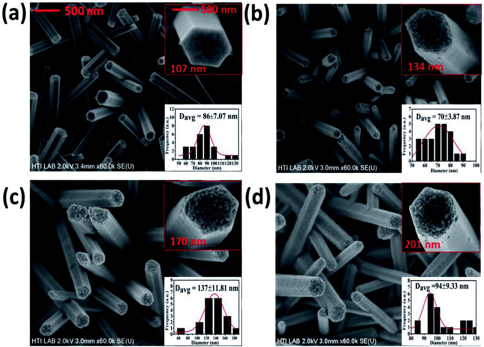 | ||
| Fig. 1 FESEM analysis of the top-down view of the (a) undoped ZnO NWs, (b) Bi:ZnO-1% NWs, (c) Bi:ZnO-3% NWs, and (d) Bi:ZnO-5% NWs. The top and bottom insets in (a)–(d) show the high-resolution image of a single nanowire and the average diameter measurements for the respective sample. | ||
In the reaction process, the hydrolysis of ZnN and HMTA occurs to release Zn2+ and OH− ions, respectively. The Zn2+ and OH− ions chemically react to form Zn(OH)2 complexes. In the growth process of the ZnO NWs, the concentration of OH− is the dominant factor contributed by HMTA. Under a given pH and temperature, Zn2+ is likely to exist as Zn(NH3)42+ and Zn(OH)42− intermediates. ZnO is formed by the dehydration of the intermediates. The oppositely charged ions produce polar surfaces, which result in a normal dipole moment and spontaneous polarization along the c-axis as well as a divergence in surface energy. The grown ZnO NWs have a preferred orientation along the c-axis due to the anisotropic crystal nature of ZnO. These hexagonal ZnO NWs are polar and have a relatively high surface energy. Consequently, the polar top planes attract a higher number of ions and promote a fast growth rate. This results in the vertical growth of the ZnO NWs on the substrate. The molecules present under the hydrothermal conditions adsorb onto the (001) surfaces and stabilize them relative to the competing facets. In the decomposition of ZnN to ZnO, the adsorbates are primarily hydroxyl groups. The growth is favoured due to the spatial preference of the reacting species. The (001) surface energy depends on the crystal thickness, and thus very thin ZnO crystals prefer the [001] orientation, which is then kinetically locked-in as growth proceeds.41
Since the Bi ions were added to the precursor solution, they induced a thermodynamic barrier in the system. The barrier slowed down the nucleation process and the growth rate of primary nuclei, which occurs on the seed layer surface, where Zn and O are arranged alternately on the top of the seed layer to nucleate a new ZnO crystal on the seeded layer. The significant tip surface roughness in Fig. 1(b)–(d) can be attributed to the diffusion of the Bi atoms. Nevertheless, the diffusion of the Bi atoms into the sidewalls is relatively less. The reason for this can be attributed to the higher surface energy at the top of the NWs, whereas that at the sidewalls is lower, as proposed by Wei et al.42 Consequently, Bi is likely to reside on the top of the NWs and deform the shape of their tip into a porous-like structure. Note that a higher doping concentration hindered the further growth of the NWs or increased their diameter because the (0001) surfaces of ZnO usually expose terminal OH− ligands in solution. The presence of valence ions instead of Zn2+ ions in the ZnO crystal is likely to enhance the adsorption of OH− ligands on the basal surfaces. These ligands will prevent the further extensive deposition of Zn-related species along the surface, leading to a decrease in the growth rate of the ZnO NWs along the c-axis.43 Likewise, it was also observed that there was a reduction in the height of the pristine ZnO NWs from 1.5 μm to 1.3 μm when doped with 1% of Bi, as shown in ESI Fig. S3-a.† As can be seen in Fig. 1, it is worth noting that even at high Bi doping concentrations, the hexagonal shape of the tip was still well-preserved without serious deformation and the nanowires were well-distributed on the substrate. This observation indicates the incorporation of the Bi ions into the ZnO matrix.
Fig. 2 shows the energy-dispersive X-ray spectroscopy (EDS) chemical compositional analysis of the pristine and Bi-doped ZnO NWs. Overall, the spectral analysis confirmed the presence of various elements, specifically Zn, O, Bi, Si, and C. The Si peak originated from the Si substrate and the appearance of C element is mainly due to the absorption of organic compounds during handling. Fig. 2(a) shows the presence of Zn and O elements in the pristine ZnO sample. When the pristine ZnO was doped with Bi atoms, the appearance of Bi peaks was observed, as shown in Fig. 2(b) and (c). It is remarkable that in Fig. 2(b) and (c), the Bi peak intensity increased when the Bi concentration increased from 1% to 3%, respectively, indicating the incorporation of Bi ions into the ZnO crystal structure. Further information on the elemental and atomic percentage of the samples is presented in ESI Table S3-b.† Fig. 2(d) presents the elemental mapping of the Bi:ZnO-3% NWs. Fig. 2(d-i) show the elemental mapping images, containing information on all the possible present elements in the Bi:ZnO-3% NWs. Fig. 2(d-ii), (d-iii), and (d-iv) in blue, green and red colours, respectively, show the further breakdown of the Bi Mα1, Zn Lα1 and O Kα1 elemental mapping. The relatively higher brightness of the Bi content on the tip surface shows that most of the Bi diffused into the tip of the nanowire, as can be seen in Fig. 2(d-ii). Besides the O element in Fig. 2(d-iv), the relatively higher brightness on the tip surface also indicates the possibility of the formation of Bi2O3. The map sum spectrum of the Bi:ZnO-3% sample in ESI Fig. S4† shows apparent ZnO and Bi peaks, further confirming the speculation of the incorporation of Bi in the ZnO lattice. Therefore, it can be concluded that the obtained EDS spectra of the pristine and Bi-doped ZnO NWs show that no other undesirable foreign elements were present in the synthesized samples.
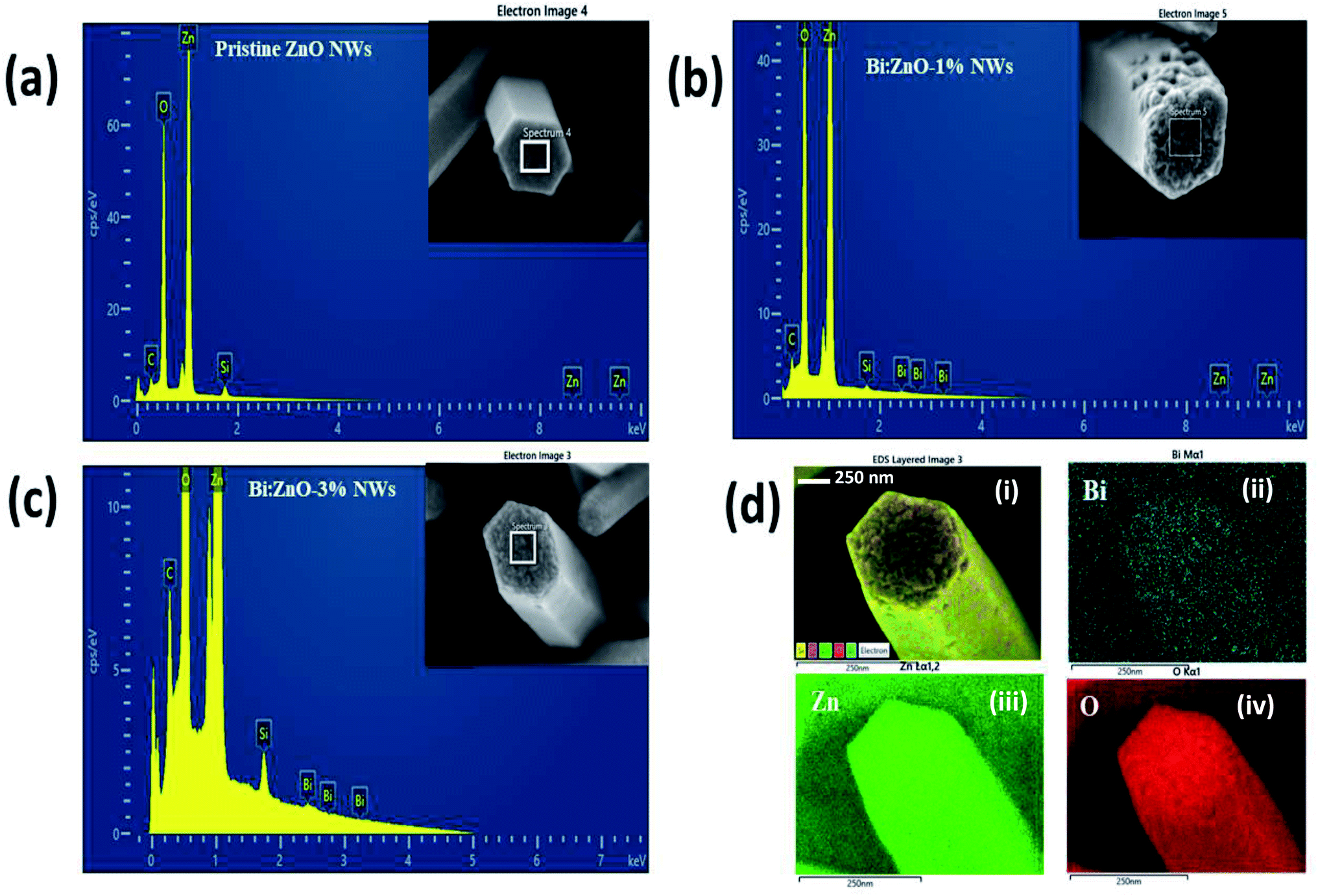 | ||
| Fig. 2 EDS analysis of (a) pristine ZnO NWs, (b) Bi:ZnO-1%, and (c) Bi:ZnO-3% NWs. (d) Elemental mapping analysis of a single Bi:ZnO-3% nanowire. | ||
Fig. 3(a) shows the TEM image of a single Bi:ZnO-3% nanowire. The inset in Fig. 3(a) shows the enlarged tip image of the nanowire marked in the red square. Fig. 3(b) shows the high-resolution-TEM (HRTEM) sidewall image of the nanowire in Fig. 3(a) at point (b). The obtained HRTEM image in Fig. 3(b) demonstrates that the prepared nanowire formed a high-quality single-crystal structure with a smooth surface and followed the [001] growth direction. The interlayer spacing, which grew along the [001] direction, was calculated to be 0.262 nm. This is in good agreement with the previously reported literature for the (002) plane of single-crystal ZnO NWs, showing that the ZnO grew vertically along the c-axis.44 The pre-deposited seed layer containing nanograins grew along the (002) polar surface, supporting the nucleation sites for the subsequent growth of the ZnO NWs.41 The NWs grew from the nucleation sites on the O-terminated (002) polar surfaces. To examine the effects of doping on different spots of the prepared Bi:ZnO-3% single nanowire, the tip and stem of the nanowire were marked as (d) and (e) in Fig. 3(c), respectively. The HRTEM images of these spots revealed that the Bi-doped ZnO crystal structure tended to become polycrystalline in nature, as can be observed in Fig. 3(d) and (e). This observation may be due to the incorporation of Bi into the ZnO lattice. However, there was no segregated cluster of impurity phases appearing throughout the nanowire.
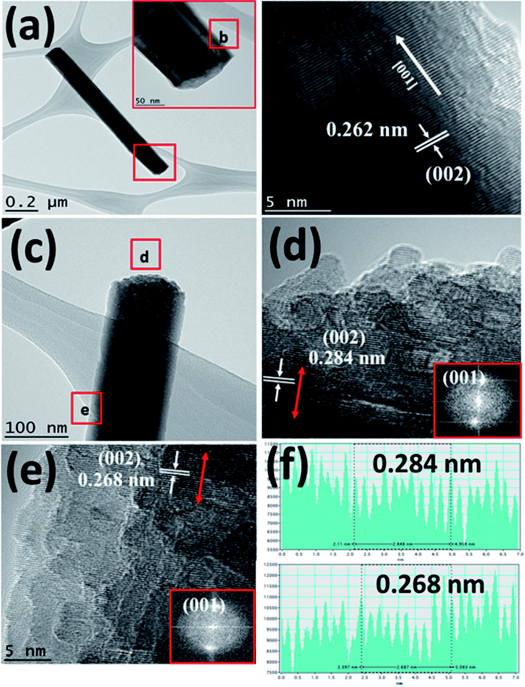 | ||
| Fig. 3 TEM images of the Bi:ZnO-3% sample. (a) A single nanowire. (b) Magnified view of the red box marked in (a). (c) Selected (d) and (e) areas at the tip and stem, respectively. (d and e) HRTEM images at the tip and stem of the nanowire, marked as (d) and (e) respectively in (c). (f) Interlayer spacing plots for (d) and (e), respectively. | ||
As discussed earlier, it is speculated that the majority of the Bi atoms tended to reside on the tip of nanowires, and a lower Bi content saturated the stem of the nanowires due to the difference in the surface energies at the tip and stem. Therefore, it is reasonable that the interlayer spacing reflects the significant changes at the tip compared to the stem of the Bi-doped ZnO NWs, as further proven by the calculated interlayer spacing values presented in Fig. 3(f). The HRTEM analysis demonstrated that the interlayer spacing between the crystal planes for the Bi-3%-doped sample was 0.284 nm at the tip of the nanowire and 0.268 nm at the edge of the stem. The measured interspacing values correspond to the (002) plane of ZnO, as shown in Fig. 3(d) and (e). The lattice expansion and change in the interlayer spacing were likely caused by Bi-doping, thus producing stress and strain in the crystal structure. Again, the increment in the lattice spacing suggests the incorporation of Bi dopant mainly in the tip area. The same behaviour is also reported in the literature when ZnO nanorods were doped with cobalt at different concentrations.45
Fig. 4(a) and (b) show the TEM EDS results measured at the tip and stem, respectively of a single nanowire. The spectra show the presence of Bi at the tip and stem of the nanowire, confirming the incorporation of 0.68 atomic percent of Bi at the tip and 0.08 atomic percent of Bi at the stem. The measurement of a higher Bi atomic percentage at the tip is more evidence to further confirm the occurrence of Bi-doping in the tip of the nanowires due to the relatively higher surface energy as compared to that of the sidewalls. Here, Bi acting as a weak base by having low positive pH accumulated more at the tip compared to the sidewalls. Due to the excess incorporation of Bi in the tip, it hindered the vertical growth along the (002) plane, and the termination of nanowire growth upon excessive Bi-doping led to the formation of Bi2O3.46 Table 1 summarizes the atomic percentage of each element present in the prepared samples.
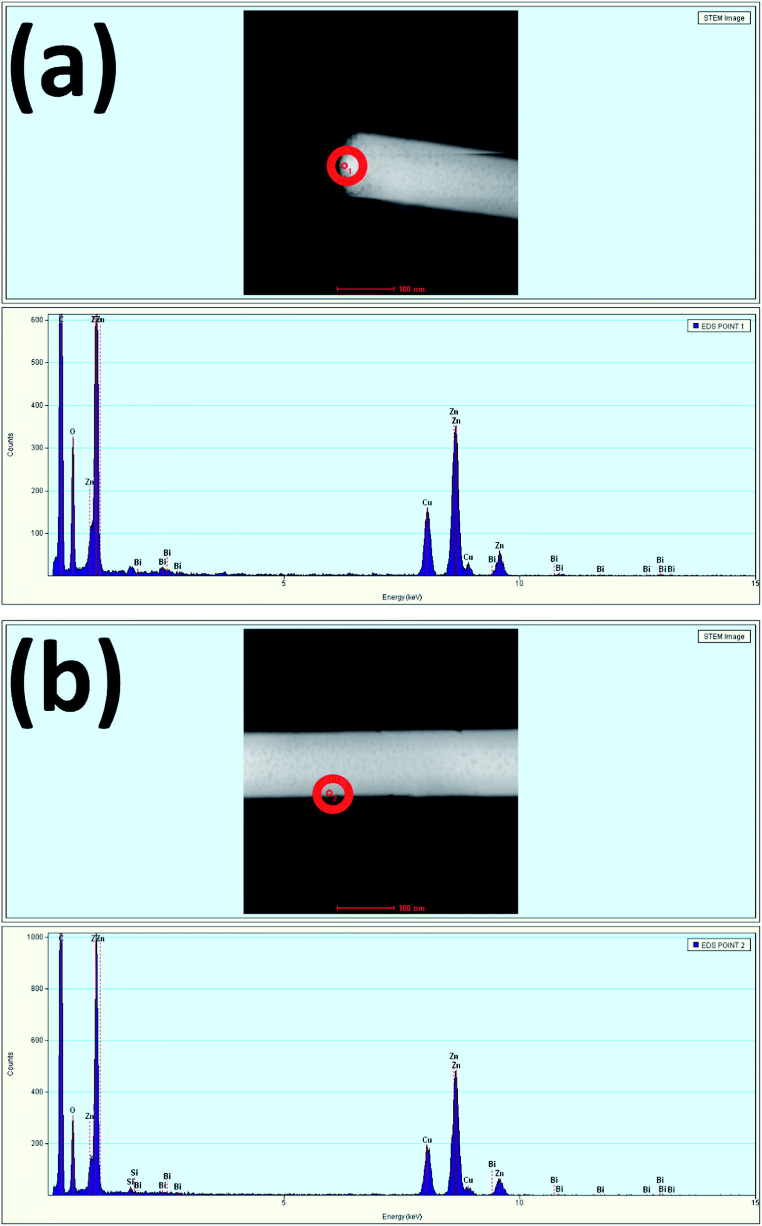 | ||
| Fig. 4 EDS spectra of Bi:ZnO-3% at the (a) tip and (b) stem of a nanowire for the selected red circle areas. | ||
| Element | Atomic percentage (%) | |
|---|---|---|
| Tip | Stem | |
| Si | 0 | 0.71 |
| O | 49.99 | 47.51 |
| Zn | 49.31 | 51.67 |
| Bi | 0.68 | 0.080 |
Fig. 5 shows the XRD patterns of the pristine and Bi-doped ZnO NWs samples. In Fig. 5(a), for the pristine ZnO, seven major peaks are observed at 32.14°, 34.46°, 36.6°, 47.92°, 56.41°, 63.24° and 68.42°, which correspond to the diffraction from the (100), (002), (101), (102), (110) (103), and (112) planes, respectively, with lattice constants of a = b = 4.24 Å and c = 5.2066 Å.47 The main peak position at 34.46° reflects the (002) plane, corresponding to the top hexagonal face. The (002) plane growth in the (001) direction along the c-axis is preferential due to crystal anisotropy, as discussed earlier, because hydrothermal complexes react to form the hexagonal crystal structure of ZnO. The narrow peak of (002) suggests the minimum full width at half maximum (FWHM) or high crystallinity. The observation of FWHM indicates the NWs are highly crystalline. The high intensity of the (002) peak provides information on the dominant reflection from the top hexagonal face of the NWs, which predominantly grew vertically along the c-axis with the hexagonal wurtzite structure. The obtained patterns are in good agreement with the presence of the hexagonal wurtzite phase crystal structure of ZnO (JCPDS # 01-075-1526). According to the patterns, upon Bi-doping into the ZnO crystal lattice, no further secondary phase and no significant changes in the XRD patterns are observed. In Fig. 5(b), it is remarkable that the intensity of the ZnO NWs is increased when the Bi-doping concentration increased from 1 to 3%. The relatively narrow and highest intensity peak of Bi–ZnO-3% as compared to the pristine ZnO and Bi–ZnO-1% samples indicate that Bi-doping increased the crystallinity of the ZnO NWs. While upon doping with Bi at 5%, the decrease in the intensity implies the slender loss of crystallinity caused by the distortion of the lattice. Bi-doping into the periodic lattice of ZnO tended to produce a small amount of strain, and consequently led to crystal regularity modification. This strain is a measure of the distortion of the lattice constants arising from crystal imperfections, especially lattice dislocation.
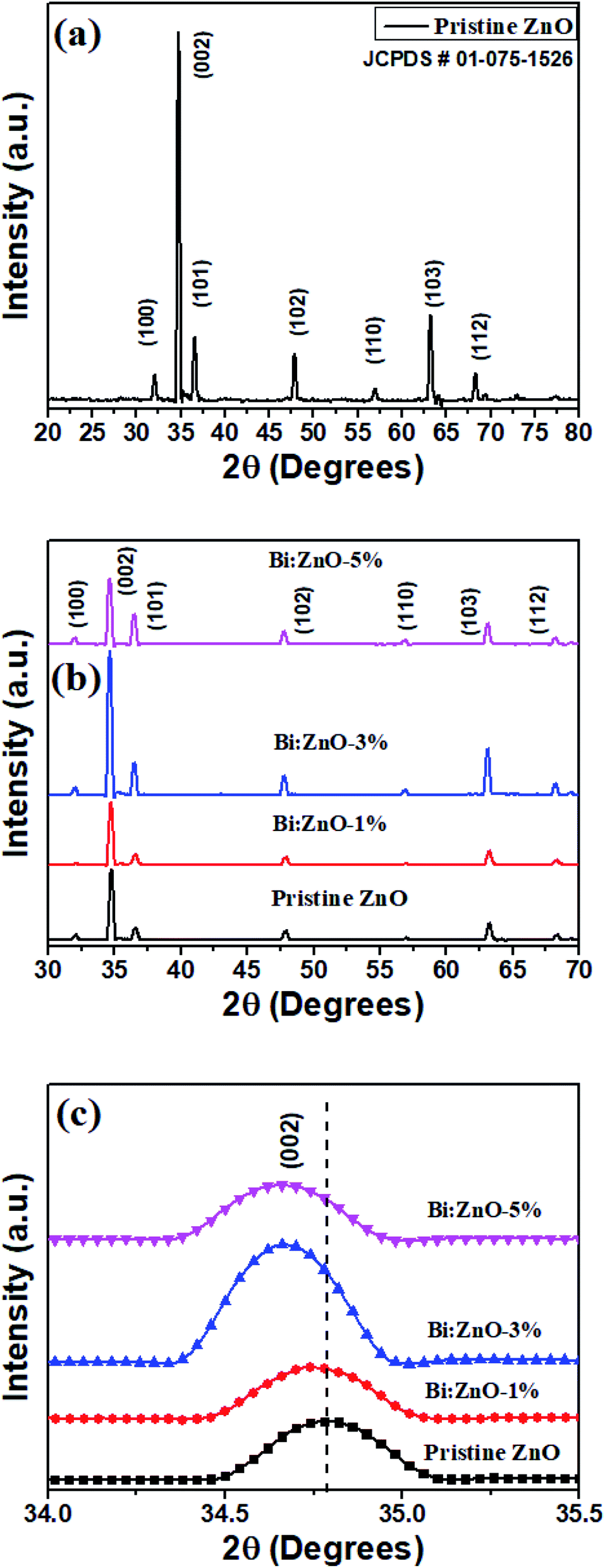 | ||
| Fig. 5 XRD analysis of (a) pristine ZnO NWs, (b) pristine and Bi-doped ZnO NWs for 1%, 3%, and 5% concentration, and (c) 002 peak for the pristine and Bi-doped ZnO NWs samples. | ||
Nevertheless, careful interpretation of Fig. 5(c) indicates that the (002) peak position shifted towards a lower angle as the Bi-doping concentration increased from 1 to 5%. Specifically, the left shift in (002) peak at 34.46° can be attributed to the difference in the atomic radii of the host and dopant, and as a result, the Zn2+ ions were substituted by Bi3+ ions. Alternatively, it is probably due to the high amount of oxygen-related defects in the ZnO NWs, in particular oxygen interstitials.48 In the case of Zn2+ being replaced by Bi3+ ions, p-type ZnO was produced with the condition that the Bi atoms merged with the substitutional oxygen sites. The merging of the Bi atoms and substitutional oxygen sites resulted in the formation of BiO acceptor defects.49 The calculated structural parameters including shift position, FWHM (β), crystalline size, Miller indices and lattice strain (ε) for the pristine and Bi-doped samples are presented in Table 2 based on Fig. 5. The crystal size and lattice strain estimation can be derived using the Debye Scherrer approach44 and ε = (βcosθ)/4,50 respectively. The average grain size for the pristine and Bi-doped ZnO NWs ranged from 39 to 43 nm. It was observed that as the Bi-doping increased, the lattice strain in the crystal structure decreased. Briefly, the Bi ions doped into the pristine ZnO lattice as substitution ions to replace Zn, forming either Bi2O3 or Bi-related oxides, and consequently polycrystalline ZnO at the top surface and sidewalls. Bi2O3 was formed between the grain boundaries, which eventually increased the lattice spacing. Nonetheless, the Bi2O3 peak was not found in the XRD patterns owing to the relatively low Bi content, which was less than 5%, as shown in the EDS characterizations in Fig. 2. The characterization of an individual nanowire using HRTEM showed its high-quality single-crystal structure in the (001) growth direction. This finding is consistent with the XRD patterns in Fig. 5.
| Sample | 2θ Position (°) | FWHM (β) | Crystalline size (nm) | (hkl) Values | Strain (ε) |
|---|---|---|---|---|---|
| Pristine ZnO | 34.78 | 0.211 | 39.27 | 002 | 0.0029 |
| Bi:ZnO-1% | 34.75 | 0.190 | 43.75 | 002 | 0.0026 |
| Bi:ZnO-3% | 34.67 | 0.189 | 43.90 | 002 | 0.0026 |
| Bi:ZnO-5% | 34.66 | 0.197 | 42.15 | 002 | 0.0028 |
X-ray photoelectron spectroscopy studies
The XPS narrow scan spectra of the pristine and Bi-doped ZnO are shown in Fig. 6. The survey scan spectra in ESI Fig. S5† indicates the presence of Zn, O, Bi, N, Na, Ca, and C. The 1s peak of C acts as a reference point, appearing in the background. In Fig. 6(a), a strong spin–orbit coupling can be observed. The Zn (2p) signal splits into two symmetrical peaks at the binding energies of 1021.75 and 1044.75 eV with the spin–orbit doublet splitting of 23 eV. The symmetrical peaks can be assigned to Zn2+ 2p3/2 and Zn2+ 2p1/2, respectively, corresponding to Zn2+ bound to oxygen in the ZnO matrix.51 Meanwhile, Fig. 6(b) shows that the binding energy of the Zn (2p) peak increased to 1021.93 and 1044.93 eV, respectively, for Bi-doping at 1% concentration in the ZnO NWs. By increasing the Bi-doping concentration up to 3%, the Zn (2p) peak binding energies decreased to 1021.65 and 1044.65 eV, respectively, as can be seen in Fig. 6(c). The O 1s peak for the pristine ZnO NWs in Fig. 6(d) shows that the asymmetric profile can be fitted into two symmetrical peaks at 530.43 and 531.69 eV, indicating the presence of two different types of oxide-related species in the sample. The oxygen peak at 530.43 eV is the lowest binding energy (OL2−) in the O1s spectrum, which can be attributed to the O2− ions in the hexagonal structure of ZnO lattice surrounded by zinc atoms. In contrast, the peak at 531.69 eV is the intermediate binding energy peak (Ov) peak, which may be associated with O2− ions in the oxygen deficient regions within the matrix of ZnO. In Fig. 6(e), with Bi-doping at 1% concentration in ZnO, two new peaks are observed in the profile of O1s, a very small peak at 528.91 eV could be correlated to Bi2O3. Another significant peak known as the higher binding energy peak (OOH) appeared at 532.51 eV, which corresponds to the absorbed hydroxyl groups (–OH) on the surface, preferable at the oxygen vacancy sites of the NWs.52 A similar trend in the peaks was also observed for Bi:ZnO-3%, as shown in Fig. 6(f). Interestingly, when the Bi-doping concentration was increased to 5%, the intensity of the small peak at 529.06 eV increased, as shown in ESI Fig. S6-ii.†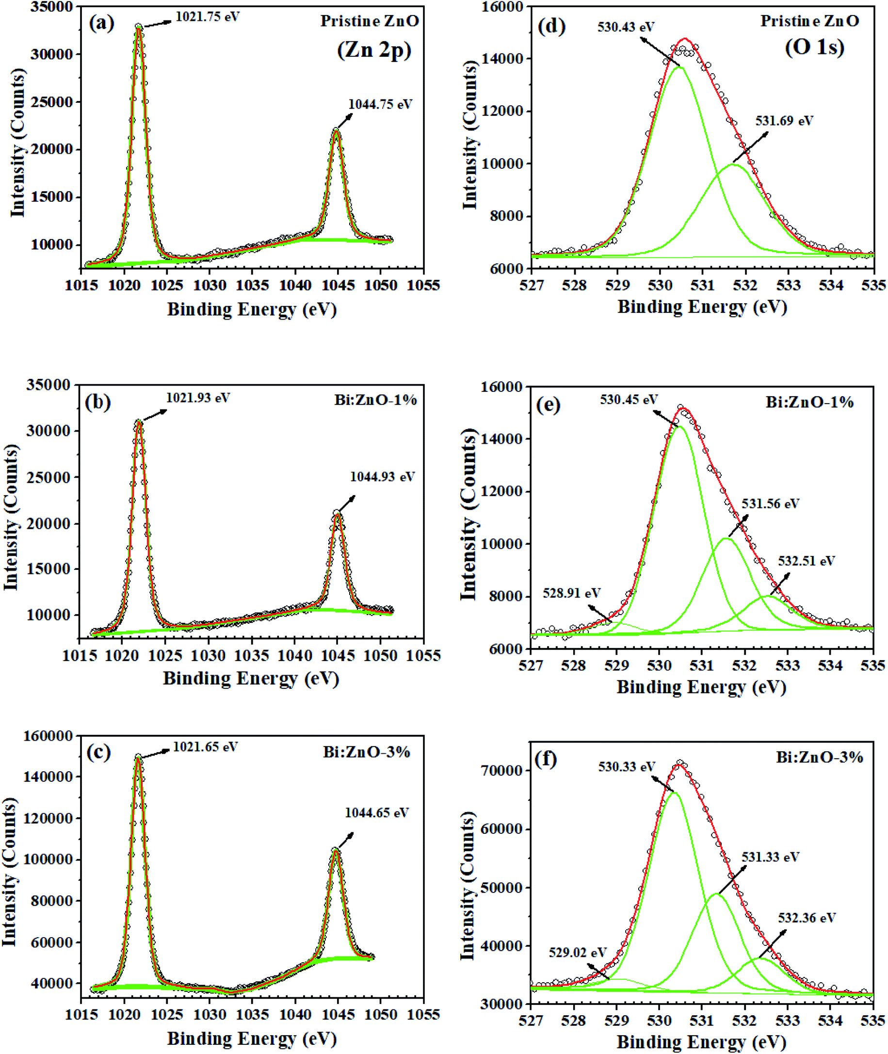 | ||
| Fig. 6 XPS characterization of the Zn element for (a) pristine ZnO, (b) Bi:ZnO-1%, and (c) Bi:ZnO-1% and O elements for (d) pristine ZnO, (e) Bi:ZnO-1%, and (f) Bi:ZnO-1%. | ||
Fig. 7(a) shows the Bi spectrum for Bi-doped at a concentration of 1% in the ZnO sample, where the peaks at the binding energy of 157.71 and 163.28 eV with a typical spin–orbit doublet splitting of 5.57 eV correspond to the binding energy of Bi 4f7/2 and Bi 4f5/2, respectively, and well-matched with Bi–metal peaks.53 While the peaks at the binding energy of 159.40 eV and 164.70 eV with the spin–orbit doublet splitting of 5.3 eV can be ascribed to the binding energy of Bi 4f7/2 and Bi 4f5/2, respectively, and these peaks match well with the Bi oxide peaks. The overall shift in the peaks of Zn (2p) and O 1s corresponds to the strain from compound replacement of Zn2+ with Bi owing to the effect of ionic radii. It should be noted that the presence of Bi2O3 is likely to be determined in the XPS analysis rather than the strain effect caused by some Zn-related ions since Bi3+ (1.03 Å) has a higher ionic radius than that of Zn2+ (0.74 Å). This may be the main reason for the formation of Bi2O3, which was detected in the XPS scan for the Bi-doped samples. Similar behaviour has been observed when Sr2+ (1.18 Å) and Ba2+ (1.35 Å) were doped in ZnO, which tended to form SrCo3 and BaCo3 carbonates, respectively.48 When the Bi-doping concentration increased from 1 to 3% as shown in Fig. 7(b), the left peak of the Bi 4f peaks (metal) shifted to a higher binding energy from 157.71 to 157.98 eV, while the other peak remained at 163.28 eV. On the contrary, further doping of 5% Bi, the Bi–metal peak intensities decreased, as shown in ESI Fig. S6,† while, in Fig. 7(b), the Bi 4f peaks (Bi2O3) at 159.40 and 164.70 eV are dominant, implying that Bi2O3 started to form in the ZnO lattice structure. The secondary oxide phase does not have any unpaired electrons and it has a zero net spin diamagnetic, resulting in the disadvantage of a reduction in the magnetic flux density of the host material.54 During the doping process, a high energy blue shift was observed for Bi 4f7/2 and Bi 4f5/2, indicating the strong interaction between Bi and ZnO, followed by the incorporation of Bi into the ZnO lattice. Thus, considering the abovementioned drawback, we opted to focus on 1% concentration of Bi-doped ZnO samples, and it is reasonable to assume 1% doping as the threshold because of the appearance of the oxide phase at a higher concentration in the obtained XPS spectrum.
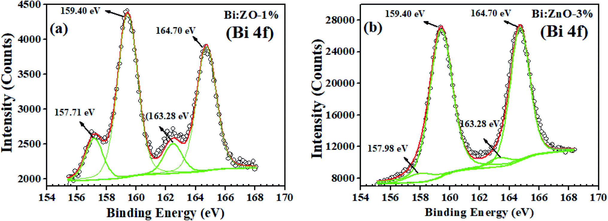 | ||
| Fig. 7 XPS characterization of (a) Bi:ZnO-1% and (b) Bi:ZnO-3% for Bi element. | ||
Optical studies
Fig. 8 shows the UV-Vis spectra of the pristine and Bi-doped ZnO NWs in the range of 300–800 nm. In Fig. 8(a), for the pristine ZnO NWs, a strong absorbance can be observed in the vicinity of 370 nm (3.35 eV), whereas no significant absorption is observed in the visible region for all the pristine and Bi-doped ZnO NWs samples. The probable explanation for this is the large absorption of incident photon energy by the electrons in the valence states present in the low energy state. In this case, the excited electrons gained sufficient energy to transfer to higher energy states. The strong absorption peaks observed at 370, 380, 375, and 377 nm correspond to the optical bandgap of 3.35, 3.26, 3.30, and 3.28 eV for the pristine, 1, 3, and 5%-doped ZnO NWs samples, respectively, implying a red shift, i.e., to a higher wavelength. The optical bandgap was determined using the Tauc equation, as reported elsewhere.45 A red shift is observed when Bi-doping creates allowed energy states within the bandgap and tends to reduce the optical bandgap of ZnO NWs. The reduction in optical bandgap for the Bi:ZnO samples at 1, 3 and 5% may be affected by the sp–d exchange interaction between the localized d-electrons and band electrons of the Bi ions during the incorporation of the Bi ions into the ZnO lattice.55 As mentioned previously, the Bi-doped ZnO nanostructures show p-type behaviour and the pristine ZnO NWs exhibit n-type properties. According to the knowledge on optical properties, the intrinsic donors in ZnO exist in the form of interstitial zinc atoms and undesired dopants. Therefore, the holes produced by the acceptors were compensated by the native imperfections of ZnO and hindered the p-type doping. Another p-type doping explanation may be the merging of the cationic atoms and substitutional oxygen sites, forming acceptor defects.49 However, the assumption of p-type doping is still a debate. Fig. 8(b) shows the Tauc plots for the optical bandgap (Eg) of the pristine and Bi-doped ZnO NWs.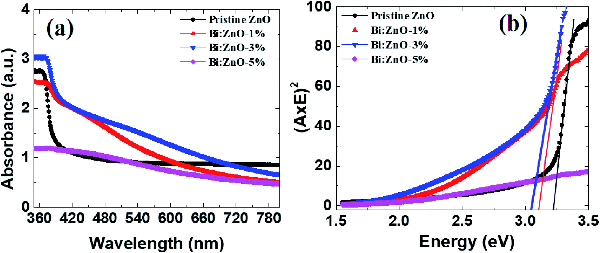 | ||
| Fig. 8 (a) UV-Vis analysis of the absorption spectra, and (b) Tauc plot for the pristine and Bi-doped samples. | ||
Fig. 9 shows the fitted PL spectra of the pristine and Bi-doped ZnO NWs in the range of 300–900 nm. Fig. 9(a) shows the enlarged UV emission behavior in the 381–393 nm region. In the fitted spectra in Fig. 9(b–e), two obvious PL regions can be observed for the pure and Bi-doped ZnO samples. The first region corresponds to the UV emission band in the range of 381–393 nm, as presented in Fig. 9(a), which shows the spectra in the range of 360–420 nm, and the other is from 450–780 nm in the visible spectrum region. The UV emission peak is ascribed to the excitonic emission from the near-band-edge transition of the wide bandgap of ZnO during the recombination of free excitons through an exciton–exciton process.56 The origin of the broad visible emission band in the range of 450–780 nm is attributed to the tunneling of surface-bound electrons through pre-existing trapped holes formed by surface anion vacancies, oxygen vacancies, or oxygen-related interface or surface states.57 The signature of the excitonic band was observed at 381 nm for the pure ZnO NWs. However, upon doping with Bi at different concentrations (1, 3, and 5%), this peak red-shifted to 382, 384.6, and 393 nm, respectively. The bandgap based on the PL spectra for the pure, 1, 3, and 5% Bi-doped ZnO NWs was estimated to be 3.25, 3.24, 3.22, and 3.15 eV, respectively. The estimated bandgaps using the PL method are slightly lower than that from UV-Vis estimation in Fig. 8. This minor uncertainty in both measurements is expected since a lower intensity xenon source was used in the UV-Vis measurements. In addition, the laser source in the PL system emitted higher energy wavelengths to separate all the transitions, which occurs at the atomic scale. It is interesting to note that the magnetism in ZnO is commonly attributed to defects, either intrinsic especially oxygen vacancies or doping-induced defects. Nevertheless, according to the PL studies, as shown in Fig. 9, the strong increase in emission in the visible region when the Bi concentration increased beyond 1% can be ascribed to the increase in defect density with an increase in Bi-doping concentration; however, the magnetism decreased. It is also noticeable that the number of defect-related peaks in the pure ZnO is higher than that for the doped sample. Even though the intensity of the emission is larger for the doped sample in the visible region, the increase in intensity in the visible region after doping is plausible due to the formation of Bi2O3, not defects. This assumption of the formation of bismuth oxide was further proven by XPS studies, as shown in Fig. S6.† Therefore, Bi-doping does not appear to increase the concentration of oxygen defects, but introducing Bi in the crystal may result in doping in already available oxygen vacancies (ZnBixO1−x) and produces bismuth oxide at a higher doping concentration.
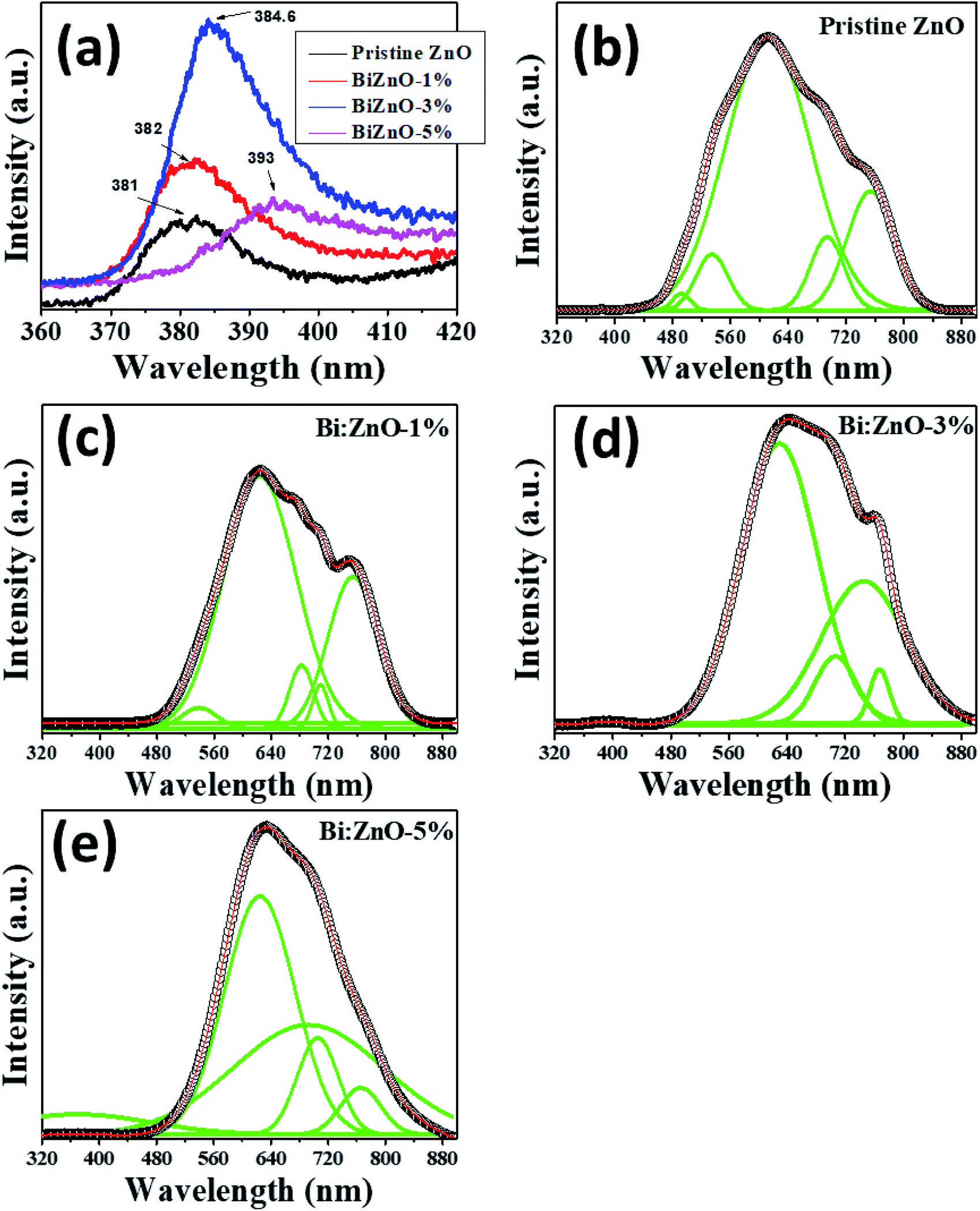 | ||
| Fig. 9 PL analysis of (a) pristine and Bi-doped ZnO NWs in the range of 360–420 nm, and (b) pristine ZnO, (c) Bi:ZnO-1%, (d) Bi:ZnO-3%, and (e) Bi:ZnO-5% in the range of 320–880 nm. | ||
Magnetic properties
Fig. 10 shows the magnetization curves of the pristine and Bi-doped ZnO NWs samples measured at 300 and 4 K at 60 kOe using a super conducting quantum interference device. Fig. 10(a) shows the magnetization versus magnetic field (M–H) curve for the pristine ZnO samples. The sample at 300 K has saturation magnetization (Ms) at 1 kOe while it has an Ms value of 5 kOe at 4 K. In Fig. 10(b), for the Bi:ZnO-1% sample, at 300 and 4 K it has an Ms value of 5 and 1.5 kOe, respectively. It is noticeable that by doping Bi, the saturation magnetization of the sample at low temperature was significantly reduced. However, when the Bi-doping concentration increased to 3%, as seen in Fig. 10(c), the sample showed a poor magnetic response due to the appearance of Bi2O3 in the crystal lattice of ZnO, which was confirmed by the XPS analysis in Fig. 7(b). The previous reports on sputtered and pristine ZnO thin films show diamagnetic behaviour,58,59 but contradict our finding that the pristine ZnO NWs show ferromagnetic behaviour. This is understandable since NWs have a large surface to volume ratio and relatively more surface defects, hence ferromagnetic behaviour, unlike thin films. The nature of this ferromagnetic behaviour is unstable due to the on-going oxidation process on the surface of the NWs.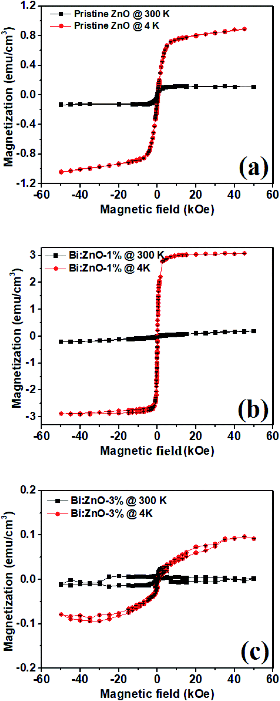 | ||
| Fig. 10 SQUID plots at 300 K (close squares) and 4 K (closed circles) for (a) pristine ZnO, (b) Bi:ZnO-1%, and (c) Bi:ZnO-3% NWs. | ||
The high surface to volume ratio and intrinsic defects in ZnO nanostructures generate a large number of uncompensated surface spins and gives rise to long-range ferromagnetic order.60 The ferromagnetism behaviour of the pristine ZnO NWs is controlled by the residual ferromagnetic impurities, which exist in the form of Zn interstitials and O vacancies. When the ZnO samples were doped with different Bi concentrations, the magnetic moment per Bi atom increased with an increase in Bi concentration. Due to the increase in the magnetic moment of the Bi atoms, the distance between the dopant and the neighbouring O atoms generally decreases and exchange coupling becomes stronger. There have been reports about ZnO doping with Bi,1,61,62 which indicate that doping will introduce acceptor levels in the bandgap, turning ZnO into p-type.63 The narrowing of the bandgap observed in the Bi-doped ZnO samples in this work is also reflected in the UV-Visible absorption spectra, as shown in Fig. 8, corresponding to the introduction of acceptor levels near the valence band. Bismuth being pentavalent will be incorporated in the O site as an anion and introduce acceptor levels, thus introducing holes in the crystal. Moreover, Bi([Xe]4f145d106s26p3), Zn([Ar]3d104s2) and O([He]2s22p4) have ionic radii of 0.11 nm, 0.074 nm, and 0.140 nm, respectively, and thus, most likely the Bi will be incorporated in the O sites with a large ionic radii.64 Doping of Bi will introduce acceptor levels due to its p-orbital, and hence free holes in the crystal. The free carriers in the localized orbitals are responsible for the itinerant magnetism in metals. The Bi p-orbital is relatively localized, and therefore gives rise to p–p coupling. Therefore, the free holes and the p–p orbital coupling between the host and Bi dopant are responsible for the enhanced ferromagnetic behaviour. This ferromagnetic behaviour observed in the Bi-doped ZnO NWs shows that the p–p interaction in the anion-doped DMS has a long-range characteristic.
The temperature vs. magnetization (M–T) properties of the pristine ZnO, 1 and 3%-doped samples are shown in ESI Fig. S7.† The higher temperature diamagnetic contribution and paramagnetic contribution was subtracted from the data. In Fig. S7,† it is obvious that there is no magnetic phase transition in the temperature range of 20 to 300 K even though in the pristine sample the magnetization seemed to decrease near 250 K, but in the case of the 1 and 3%-doped samples it remained essentially constant in the whole temperature range. Moreover, compared with the pristine and 3%-doped samples the magnetization in the 1%-doped sample was higher in the entire temperature range, which is considerably expected from the M–H curves, as shown in Fig. 10. All the samples remained ferromagnetic until room temperature and even higher. It was observed that these materials have a Curie temperature much higher than room temperature. This suggests that Bi-doped ZnO nanowires can be integrated into next-generation room temperature-operated spintronic-based switching devices.
Conclusions
In conclusion, our proposed hydrothermal method is novel, inexpensive, and promising to prepare highly crystalline Bi-doped ZnO NWs at low temperature without the requirement of a costly vacuum environment. The electronic and magnetic properties of the anion-doped DMS are associated with the localized p-orbital and free carriers introduced in the system by the doping approach. The presence of Bi atoms doped in the ZnO crystal lattice was verified by FESEM, TEM, and XPS characterizations. Then, UV-Vis analysis and PL spectral measurement demonstrated that the optical bandgap decreased with an increase in Bi concentration. The XRD results showed the same findings as the TEM analysis of the formation of highly crystalline hexagonal ZnO samples in the absence and presence of Bi-doping. The SQUID measurements showed that the Bi 1%-doped sample showed improved saturation magnetization compared to the pristine ZnO sample. The origin of the ferromagnetism in the Bi-doped ZnO samples is believed to be caused by the p–p coupling interaction among the zinc, bismuth, and oxygen atoms. The induced stable ferromagnetism behaviour by the dopant is highly dependent on the spin–orbit coupling and p–p interaction. Since saturation magnetization can be achieved at low applied magnetic fields for the Bi-doped samples, they are beneficial for fast switching spin-FETs devices since their high crystallinity will ensure high mobility and ultimately speedy spintronics devices.Conflicts of interest
There are no conflicts to declare.Acknowledgements
This work was supported in part by the Ministry of Higher Education Malaysia, Fundamental Research Grant Scheme (FRGS/1/2017/STG07/UKM/02/6), (FP114-2019A), Universiti Kebangsaan Malaysia grants DIP 2019-018 and GGPM-2019-032.References
- J. Lee, N. G. Subramaniam, I. A. Kowalik, J. Nisar, J. Lee, Y. Kwon, J. Lee, T. Kang, X. Peng, D. Arvanitis and R. Ahuja, Sci. Rep., 2015, 5, 1–10 Search PubMed.
- T. Thangeeswari, J. Velmurugan and M. Priya, J. Mater. Sci. Mater. Electron., 2013, 24, 4817–4826 CrossRef CAS.
- A. Hirohata and K. Takanashi, J. Phys. D. Appl. Phys., 2014, 47(19), 193001 CrossRef.
- W. Oelerich, T. Klassen and R. Bormann, J. Alloys Compd., 2001, 315, 237–242 CrossRef CAS.
- K. Nagaveni, M. S. Hegde, N. Ravishankar, G. N. Subbanna and G. Madras, Langmuir, 2004, 20, 2900–2907 CrossRef CAS.
- G. A. Mutch, S. Shulda, A. J. McCue, M. J. Menart, C. V. Ciobanu, C. Ngo, J. A. Anderson, R. M. Richards and D. Vega-Maza, J. Am. Chem. Soc., 2018, 140, 4736–4742 CrossRef CAS PubMed.
- H. Lee, J. Lim, C. Lee, S. Back, K. An, J. W. Shin, R. Ryoo, Y. Jung and J. Y. Park, Nat. Commun., 2018, 9, 1–8 CrossRef PubMed.
- Y. Liu, R. Ran, M. O. Tade and Z. Shao, J. Memb. Sci., 2014, 467, 100–108 CrossRef CAS.
- E. Fabbri, D. Pergolesi and E. Traversa, Chem. Soc. Rev., 2010, 39, 4355–4369 RSC.
- Z. Xu, Y. Liu, W. Zhou, M. O. Tade and Z. Shao, ACS Appl. Mater. Interfaces, 2018, 10, 9415–9423 CrossRef CAS PubMed.
- Y. Liu, Y. Guo, R. Ran and Z. Shao, J. Memb. Sci., 2012, 415–416, 391–398 CrossRef CAS.
- S. Abed, K. Bouchouit, M. S. Aida, S. Taboukhat, Z. Sofiani, B. Kulyk and V. Figa, Opt. Mater. (Amst)., 2016, 56, 40–44 CrossRef CAS.
- J. M. Li, CrystEngComm, 2017, 19, 32–39 RSC.
- M. Samadi, M. Zirak, A. Naseri, E. Khorashadizade and A. Z. Moshfegh, Thin Solid Films, 2016, 605, 2–19 CrossRef CAS.
- M. A. Mohamed, P. T. Lam, K. W. Bae and N. Otsuka, J. Appl. Phys., 2011, 110(12), 123716 CrossRef.
- K. W. Bae, M. A. Mohamed, D. W. Jung and N. Otsuka, J. Appl. Phys., 2011, 109(7), 073918 CrossRef.
- S. J. Pearton, D. P. Norton, M. P. Ivill, A. F. Hebard, J. M. Zavada, W. M. Chen and I. A. Buyanova, J. Electron. Mater., 2007, 36, 462–471 CrossRef CAS.
- Y. Zhang, W. Liu and H. Niu, Solid State Commun., 2008, 145, 590–593 CrossRef CAS.
- H. Pan, J. B. Yi, L. Shen, R. Q. Wu, J. H. Yang, J. Y. Lin, Y. P. Feng, J. Ding, L. H. Van and J. H. Yin, Phys. Rev. Lett., 2007, 99, 1–4 CrossRef PubMed.
- J. M. Li, X. L. Zeng, G. Q. Wu and Z. A. Xu, CrystEngComm, 2012, 14, 525–532 RSC.
- J. M. Li and X. L. Zeng, Appl. Phys. Lett., 2017, 110, 5 Search PubMed.
- J. M. Li, X. L. Zeng, D. P. Wei, Y. B. Hu and Z. A. Xu, ACS Appl. Mater. Interfaces, 2014, 6, 4490–4497 CrossRef CAS.
- D. B. Buchholz, R. P. H. Chang, J. Y. Song and J. B. Ketterson, Appl. Phys. Lett., 2005, 87, 8–11 Search PubMed.
- H. J. Lee, S. Y. Jeong, C. R. Cho and C. H. Park, Appl. Phys. Lett., 2002, 81, 4020–4022 CrossRef CAS.
- X. Peng and R. Ahuja, Appl. Phys. Lett., 2009, 94, 1–4 Search PubMed.
- Y. Lin, S. Lin, M. Luo and J. Liu, Mater. Lett., 2009, 63, 1169–1171 CrossRef CAS.
- J. Liu and O. V. Prezhdo, J. Phys. Chem. Lett., 2015, 6, 4463–4469 CrossRef CAS PubMed.
- M. V. Konishcheva, D. I. Potemkin, P. V. Snytnikov, O. A. Stonkus, V. D. Belyaev and V. A. Sobyanin, Appl. Catal. B Environ., 2018, 221, 413–421 CrossRef CAS.
- D. Dogu, K. E. Meyer, A. Fuller, S. Gunduz, D. J. Deka, N. Kramer, A. C. Co and U. S. Ozkan, Appl. Catal. B Environ., 2018, 227, 90–101 CrossRef CAS.
- E. Chikoidze, M. Nolan, M. Modreanu, V. Sallet and P. Galtier, Thin Solid Films, 2008, 516, 8146–8149 CrossRef CAS.
- X. Li, F. Kang, W. Shen and X. Bai, Electrochim. Acta, 2007, 53, 1761–1765 CrossRef CAS.
- P. Sharma, A. Gupta, K. V. Rao, F. J. Owens, R. Sharma, R. Ahuja, J. M. O. Guillen, B. Johansson and G. A. Gehring, Nat. Mater., 2003, 2, 673–677 CrossRef CAS PubMed.
- X. Tan, C. Chen, K. Jin and Y. Gao, Phys. B Condens. Matter, 2013, 412, 91–93 CrossRef CAS.
- D. T. Ngo, L. T. Cuong, N. H. Cuong, C. T. Son, P. T. Huy and N. D. Dung, Adv. Funct. Mater., 2018, 28, 1–6 CrossRef.
- Y. Liu, H. Zhang, Q. Zhao, Q. Lu, M. Zhu and M. Zhang, Phys. Chem. Chem. Phys., 2019, 15089–15096 RSC.
- Y. Jin, N. Zhang, H. Xu and B. Zhang, Appl. Phys. Lett., 2018, 113(20), 202401 CrossRef.
- M. Z. Shoushtari, A. Emami and S. E. M. Ghahfarokhi, J. Magn. Magn. Mater., 2016, 419, 572–579 CrossRef CAS.
- T. Fangsuwannarak, P. Krongarrom, J. Kaewphoka and S. T. Rattanachan, 10th Int. Conf. Electr. Eng. Comput. Telecommun. Inf. Technol. ECTI-CON 2013, 2013, DOI:10.1109/ECTICon.2013.6559582.
- K. Sedeek, E. Abdeltwab, H. Hantour and N. Makram, J. Supercond. Nov. Magn., 2020, 33, 445–453 CrossRef CAS.
- M. Aras, S. Güler-Klllç and Ç. Klllç, Phys. Rev. B, 2017, 95, 1–8 Search PubMed.
- F. Solís-Pomar, E. Martínez, M. F. Meléndrez and E. Pérez-Tijerina, Nanoscale Res. Lett., 2011, 6, 1–11 Search PubMed.
- W. Wu, Q. He and C. Jiang, Nanoscale Res. Lett., 2008, 3, 397–415 CrossRef CAS PubMed.
- R. Zamiri, A. F. Lemos, A. Reblo, H. A. Ahangar and J. M. F. Ferreira, Ceram. Int., 2014, 40, 523–529 CrossRef CAS.
- S. S. A. Karim, Y. Takamura, P. T. Tue, N. T. Tung, J. Kazmi and C. F. Dee, Materials, 2020, 13(5), 1136 CrossRef PubMed.
- A. Chanda, S. Gupta, M. Vasundhara, S. R. Joshi, G. R. Mutta and J. Singh, RSC Adv., 2017, 7, 50527–50536 RSC.
- C. Xu, K. Rho, J. Chun and D. E. Kim, Nanotechnology, 2006, 17, 60–64 CrossRef CAS.
- R. Joshi, P. Kumar, A. Gaur and K. Asokan, Appl. Nanosci., 2014, 4, 531–536 CrossRef CAS.
- A. S. H. Hameed, C. Karthikeyan, S. Sasikumar, V. Senthil Kumar, S. Kumaresan and G. Ravi, J. Mater. Chem. B, 2013, 1, 5950–5962 RSC.
- K. Tang, S. L. Gu, J. D. Ye, S. M. Zhu, R. Zhang and Y. D. Zheng, Chinese Phys. B, 2017, 26, 1–23 Search PubMed.
- P. Bindu and S. Thomas, J. Theor. Appl. Phys., 2014, 8, 123–134 CrossRef.
- Q. Liu, J. Huan, N. Hao, J. Qian, H. Mao and K. Wang, ACS Appl. Mater. Interfaces, 2017, 9, 18369–18376 CrossRef CAS PubMed.
- S. Dhara, K. Imakita, M. Mizuhata and M. Fujii, Nanotechnology, 2014, 25(22), 225202 CrossRef PubMed.
- S. Bera, S. Ghosh and R. N. Basu, New J. Chem., 2018, 42, 541–554 RSC.
- O. Madelung, U. Rössler and M. Schulz, II-VI and I-VII compounds; semimagnetic compounds, Springer-Verlag, Berlin Heidelberg, 1999, vol. 41, pp. 1–5 Search PubMed.
- S. Shi, Y. Yang, J. Xu, L. Li, X. Zhang, G. H. Hu and Z. M. Dang, J. Alloys Compd., 2013, 576, 59–65 CrossRef CAS.
- L. Wang and N. C. Giles, J. Appl. Phys., 2003, 94, 973–978 CrossRef CAS.
- N. Padmavathy and R. Vijayaraghavan, Sci. Technol. Adv. Mater., 2008, 9(3), 035004 CrossRef PubMed.
- X. Zhang, W. Zhang, X. Zhang, X. Xu, F. Meng and C. C. Tang, Adv. Condens. Matter Phys., 2014, 2014, 1 Search PubMed.
- N. C. Mamani, R. T. da Silva, A. O. de Zevallos, A. A. C. Cotta, W. A. de A. Macedo, M. S. Li, M. I. B. Bernardi, A. C. Doriguetto and H. B. de Carvalho, J. Alloys Compd., 2017, 695, 2682–2688 CrossRef CAS.
- K. Thiyagarajan, M. Muralidharan and K. Sivakumar, J. Mater. Sci. Mater. Electron., 2018, 29, 7442–7452 CrossRef CAS.
- V. L. Chandraboss, L. Natanapatham, B. Karthikeyan, J. Kamalakkannan, S. Prabha and S. Senthilvelan, Mater. Res. Bull., 2013, 48, 3707–3712 CrossRef CAS.
- E. F. Keskenler, S. Aydin, G. Turgut and S. Doʇan, Acta Phys. Pol. A, 2014, 126, 782–786 CrossRef CAS.
- J. W. Lee, N. G. Subramaniam, J. C. Lee, S. Kumar S and T. W. Kang, Europhys. Lett., 2011, 95(4), 47002 CrossRef.
- O. Methods, Edition 95, 1942.
Footnote |
| † Electronic supplementary information (ESI) available: [1] Schematic diagram for preparation of ZnO nanoparticles. [2] Schematic diagram for preparation of pristine and bismuth doped ZnO nanowires. [3] Cross-sectional structure view of (a) pristine ZnO, and (b) Bi:ZnO-1% NWs. [4] FESEM (EDS) table of pristine and Bi-doped ZnO NWs. [5] Elemental mapping of Bi:ZnO-3%. [6] Survey scan XPS of pristine and Bi-doped ZnO NWs samples. [7] XPS of Bi:ZnO 5% NWs for Zn, O and Bi elements. [8] PL spectra of defect related peak at 456 nm. See DOI: 10.1039/d0ra03816d |
| This journal is © The Royal Society of Chemistry 2020 |