DOI:
10.1039/D0RA03372C
(Paper)
RSC Adv., 2020,
10, 22996-23001
Quantification of defects engineered in single layer MoS2†
Received
15th April 2020
, Accepted 6th June 2020
First published on 16th June 2020
Abstract
Atomic defects are controllably introduced in suspended single layer molybdenum disulfide (1L MoS2) using helium ion beam. Vacancies exhibit one missing atom of molybdenum and a few atoms of sulfur. Quantification was done using a Scanning Transmission Electron Microscope (STEM) with an annular detector. Experimentally accessible inter-defect distance was employed to measure the degree of crystallinity in 1L MoS2. A correlation between the appearance of an acoustic phonon mode in the Raman spectra and the inter-defect distance was established, which introduces a new methodology for quantifying defects in two-dimensional materials such as MoS2.
Introduction
Monolayer molybdenum disulfide (1L MoS2) belongs to the transition metal dichalcogenide (TMDC) family and is being extensively explored for applications in next-generation electronics. In general, all TMDC materials can be represented in form of MX2 (M = Ti, Zr, Hf, V, Nb, Ta, Re, Mo, W; X = S, Se, Te), they are famous due to their ability to crystallize into layered two-dimensional (2D) structures.1–5 In this case, the 2D MoS2 crystal is made up of a molybdenum atomic layer sandwiched between two atomic layers of closely packed sulfur atoms. 1L MoS2 has demonstrated several unique optical and optoelectronic properties for a wide range of applications.2,6–10 Furthermore, 1L MoS2, being a direct bandgap semiconductor, opens up the possibility for energy-efficient field effect transistors, photodetectors, solar cells and other optoelectronic devices. However, the practicability of realizing these applications hinges upon the synthesis of high quality, large area of MoS2 monolayers. Large area and high-quality 1L MoS2 can be made by using Chemical Vapor Deposition (CVD). Yet when compared to mechanical exfoliated samples, the CVD grown monolayers usually have lower carrier mobility due to inherent defects such as sulfur vacancies introduced during the growth process.11,12 It has been reported that these structural defects in 1L MoS2 can influence the mechanical, optical and electrical properties of the material13 due to local modification of MoS2 band structure in the vicinity of the defected spots.14 Also, several approaches have been reported in literature for creating and controlling density of sulfur vacancies by using electron or ion irradiation, thermal annealing and plasma treatment.15–18 The development of these methods is crucial and intensely under investigation for controlling the material properties to match the requirements in different applications. It has been reported that Raman spectroscopy has emerged a powerful nondestructive characterization tool to quantify the defects controllably created in 1L MoS2 by calculation the inter-defect distance (LD).19 The characteristic (E2g, A1g) peaks of the Raman active modes broaden with increasing defect density. This is accompanied by a downshift of the position of the E2g peak and an upshift of the position of the A1g peak.20–23 With the increase in vacancy concentration, there are fewer Mo–S bonds involved in the in-plane vibration; therefore, the E2g peak is weakened and red shifted. The A1g peak corresponds to the out-of-plane vibration of Mo–S bonds with the Mo atom as a static center for 1L MoS2. The restoring force constant is reduced because of missing Mo–S bond. Therefore, the originally static Mo atom is allowed to vibrate out-of-plane, which strengthens the restoring force constant from Mo–S vibration. This results in the blueshift of the A1g peak. Additionally, we expect appearance of the longitudinal acoustic mode peak at 227 cm−1 which is attributed to disorder-induced Raman scattering with momentum q ≠ 0 at M point.
In this article, we report on using helium ion irradiation, to controllably introduce defects in 1L MoS2 and then, we quantify the degree of crystallinity of 1L MoS2 using Scanning Transmission Electron Microscope (STEM) and Raman spectroscopy. We have also investigated the correlation between ratio of Longitudinal Acoustic (LA) Raman active mode with respect to transverse optical A1g Raman mode and the experimentally accessible inter-defect distance from STEM analysis.
Experimental
The MoS2 was grown on Si/SiO2 substrate on a home-built chemical vapor deposition (CVD) system. Synthesis was optimized wherein molybdenum(VI) oxide and sulfur precursors react in vapor phase to deposit 1–2 layers of high quality MoS2 monolayers (thickness ∼ 1 nm). Zeiss Orion Helium Ion Microscope (HeIM) was used to study the morphology and structure of MoS2. Later, using HeIM's nanofabrication mode and operating at accelerating voltage of 30 kV, MoS2 samples were irradiated. The exposure was performed using HeIM's patterning software to raster focused helium ion beam over an area varying between 10–50 μm by 10–50 μm in all single layer MoS2. A blanker current of 5 pA was used for all doses and dwell time per pixel. The Raman spectra were collected at room temperature in ambient conditions on both pristine and irradiated samples using a Horiba XploRA Raman Confocal Microscope at 532 nm wavelength excitation, with 2400 L mm−1 grating. Atomic resolution images of 1L samples transferred onto Quantaifoil TEM grids were recorded using Nion Ultra HAADF-STEM operating at 60 kV with 3rd-generation C3/C5 aberration corrector and 0.5 nA current in atomic-size probe ∼1.0–1.1 angstrom.
Results
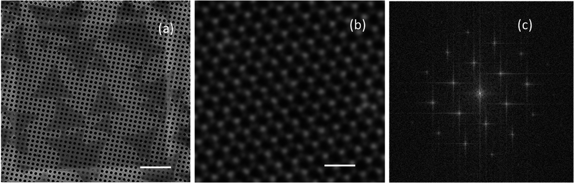
Fig. 1(a) shows a helium ion microscope image of the MoS2 sample transferred onto TEM grid using wet transfer method (see ESI†). The triangular shaped crystal is mostly single crystalline with lateral dimensions up to tens of micrometers. The atomic structure of MoS2 was studied using High angle atomic-resolution annular dark field (HAADF) imaging on the STEM. This technique is highly sensitive to variations in the atomic number of atoms in the sample; therefore, there is a significant contrast difference between molybdenum atoms of Z = 42 and sulfur atoms of Z = 16. The HAADF-STEM image shows alternating bright Mo and less bright S sites arranging in hexagonal rings in Fig. 1(b), 2(a and b). The Fourier transform of the HAADF-STEM image is presented in Fig. 1(c), with hexagonal symmetry in the Brillouin zone. The point defects such as vacancies, which are particularly observed in CVD grown MoS2 because of the growth process, can also be controllably engineered. In the STEM-HAADF image of pristine (unirradiated) sample, we can see only a few sulfur vacancies and an antisite defect, which represent vacancy complex of Mo and nearby three sulfur (MoS3) atoms. This may be due to the Mo rich environment in the growth process. We can identify antisite defects and sulfur vacancies at the lattice sites using atom-by-atom chemical analysis on the STEM-HAADF. The calculated defect density (from sulfur vacancies) in the pristine MoS2 monolayer transferred onto TEM grid was found to be 2.8 × 1013 cm−2, which agrees well with previously reported results.1 The only regions in close proximity to the edges of the MoS2 sample were significantly damaged due to imperfections in the transfer process.
 |
| | Fig. 1 (a) Helium ion image of 1L MoS2 samples transferred onto TEM grid (scale bar is 2 μm). (b) Atomic-resolution STEM-HAADF image of pristine monolayer MoS2, bright sites are molybdenum atoms and less bright sites are sulfur atoms (scale bar is 2 nm). (c) Fourier transform of the atomic structure of pristine 1L MoS2. | |
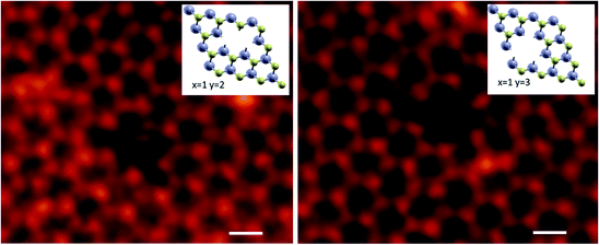 |
| | Fig. 2 High-magnification STEM images of atomic vacancies in different configurations (xMo + yS) showing single molybdenum-based vacancies at x = 1, while the number of missing sulfur atoms y varies: (a) y = 2; (b) y = 3. Scale bar is 0.3 nm. | |
Morphology and STEM-HAAF atomic structure of 1L MoS2
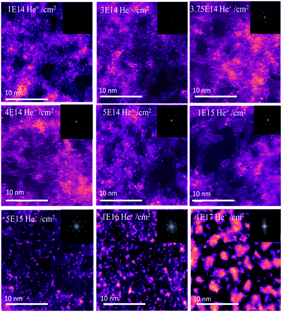
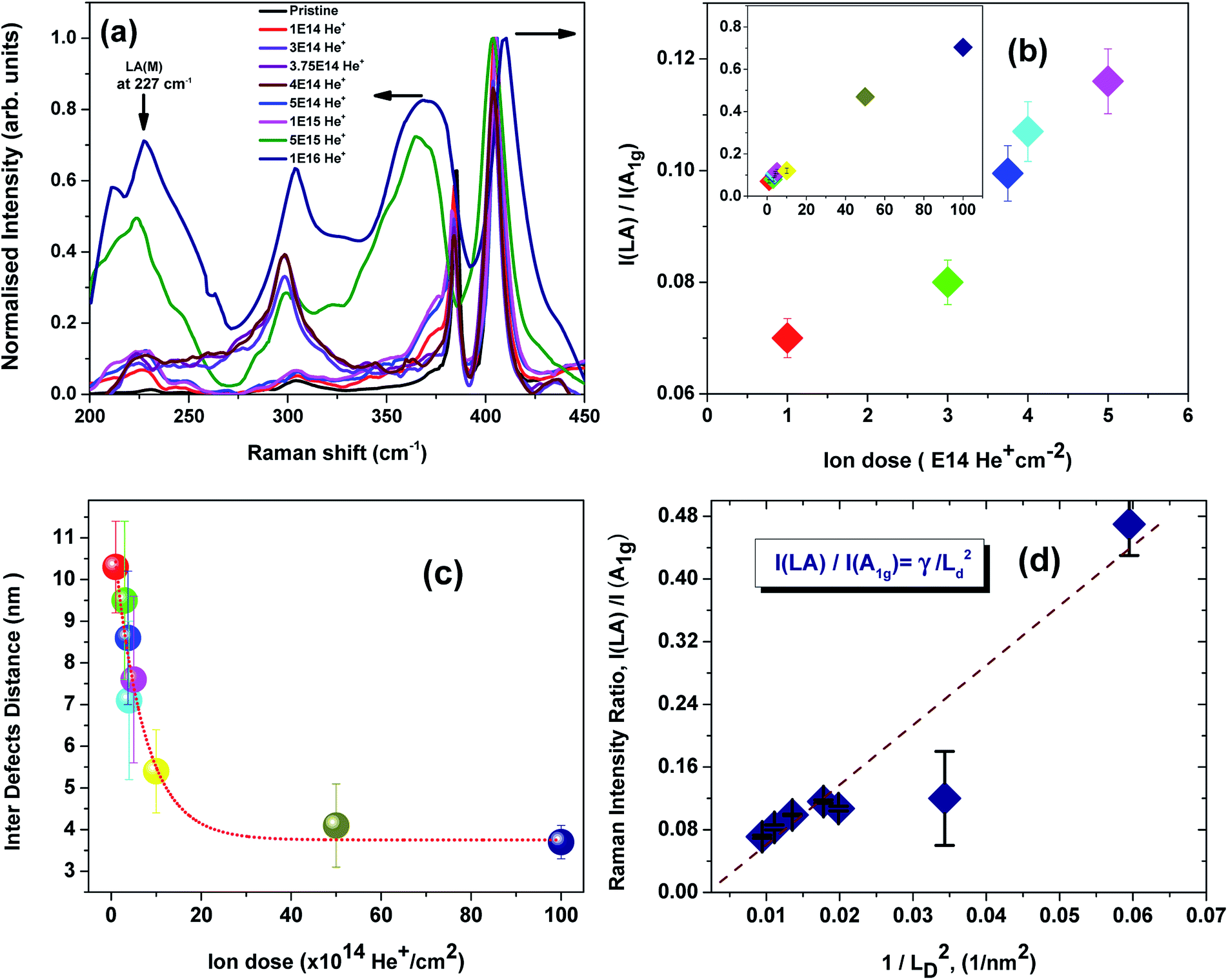
Helium ion irradiated regions on the suspended samples were identified and imaged using STEM-HAADF technique. Fig. 3 shows HAADF images of MoS2 after varying helium ion irradiation doses, namely 1 × 10¹⁴, 3 × 10¹⁴, 3.75 × 10¹⁴, 4 × 10¹⁴, 5 × 10¹⁴, 1 × 10¹⁵, 5 × 10¹⁵, 1 × 10¹⁶, and 1 × 10¹⁷ ions per cm2. The HAADF intensity allows us to distinguish elements (such as Mo and S) and the atomic structure of defects. The generated defects are consistent with the sputtering rate of helium ion beam. To assess the effect of helium ion on the metal/sulfur atomic vacancies, the experimental average inter-defect distance between two defect spots were calculated from the STEM images. The LD value was calculated manually from STEM image maps, as shown in Fig. 1S (in ESI†) for a representative dose of 1014 ions per cm2. The LD values with corresponding standard deviations for all doses are presented in Table 1. The results reveal that the degree of crystallinity of 1L MoS2 decreases as the dose increases. The predominant defects present were single molybdenum-based vacancies (1Mo + yS) while the number of missing sulfur atoms differed. Fig. 2(a) and (b) shows the smallest defect that can controllably resolved and created respectively. With increasing He+ ion dose, the number of double sulfur based vacancies (1Mo + 2S) also increased and additionally triple sulfur based vacancies (1Mo + 3S) start to appear (Fig. 2(b)). Similar results were reported for Ga+ ions at 1012 ions per cm2.24 It is important to note that the low mass of helium ions create gentle changes in crystallographic structure of 1L MoS2 compared to results reported in literature with heavier ions.25 At the highest dose of 1 × 10¹⁷ ions per cm2, the MoS2 crystal lattice is significantly distorted and damaged. The statistical analysis was performed using large area STEM images (Fig. 3) and plotted in Fig. 4(c).
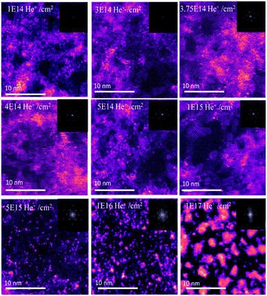 |
| | Fig. 3 Large STEM area characterization of defected 1L MoS2 with different doses of irradiation from 1 × 10¹⁴ to 1 × 10¹⁷ He+ per cm2 used to calculate LD, the FFT in insets show that sample is losing crystallinity completely at the dose 1 × 10¹⁷ He+ per cm2. | |
Table 1 The calculated value for the inter-defect distance from STEM imaging, ratio of Raman disorder, and the relation between STEM and Raman characterization
| Helium ion dose (He+ per cm2) |
LD, nm (from STEM) |

|

|
| 1 × 10¹⁴ |
10.3 ± 1.1 |
0.071 |
0.0701 |
| 3 × 10¹⁴ |
9.5 ± 1.9 |
0.083 |
0.0831 |
| 3.75 × 10¹⁴ |
8.6 ± 1.6 |
0.099 |
0.101 |
| 4 × 10¹⁴ |
7.1 ± 1.9 |
0.107 |
0.148 |
| 5 × 10¹⁴ |
7.5 ± 2.0 |
0.116 |
0.13 |
| 1 × 10¹⁵ |
5.4 ± 1.0 |
0.120 |
0.257 |
| 5 × 10¹⁵ |
4.1 ± 1.0 |
0.470 |
0.446 |
| 1 × 10¹⁶ |
3.7 ± 0.4 |
0.704 |
0.547 |
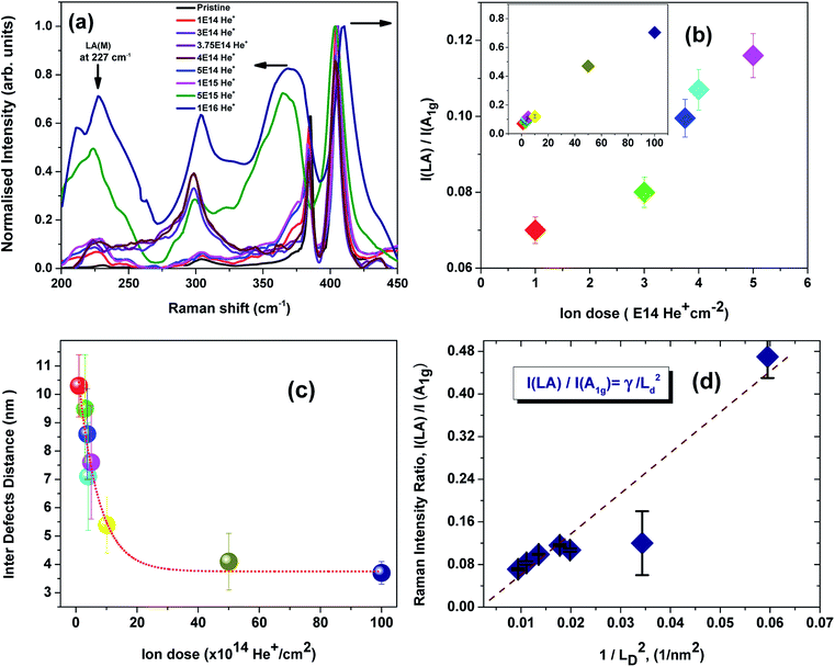 |
| | Fig. 4 (a) Raman studies of irradiated 1L MoS2 on silicon substrate; the first order Raman modes (E2g/A1g) are red/blue shifted and the second order mode LA(M) arises upon dosage increase; a peak at 300 cm−1 is related to Si acoustic mode; (b) ratio of intensity of longitudinal acoustic mode versus out of plane vibration mode of 1L MoS2 for doses up to 5 × 10¹⁵ He+ per cm2, the whole range of doses vs. ratio presented in the inset; (c) plot of calculated inter defect distance versus helium ion dose from STEM characterization; (d) correlation between the inter-defect distance and Raman data for 1L MoS2. | |
Defect characterization of 1L MoS2
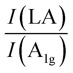
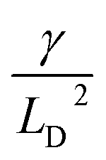
Fourier transform of the STEM images following helium irradiation in the suspended MoS2 samples reveals the crystallographic nature of MoS2 (Fig. 3 insets). The broadening of diffraction spots with increase in dose from 1 × 10¹⁵ He+ per cm2 to 1 × 10¹⁷ He+ per cm2 is representation of breaking of the crystal symmetry and periodicity due to random scattering events and broadened Bragg diffraction.26 The crystallinity of MoS2 is intact for helium ion doses below 1 × 10¹⁵ ions per cm2. Raman spectroscopy was additionally used to investigate the disorder effect in 1L MoS2. For Raman characterization, we irradiated MoS2 on Si substrate (the original growth substrate) with the same doses as used in the STEM-HAADF analysis. The results were identical to Raman characterization of suspended MoS2 (see ESI†). Similar to the previously reported data,20 (in-plane E2g)/(out-of-plane A1g) vibrational modes were red/blue shifted and both modes broadened after helium irradiation. In addition, a shoulder (at around 362 cm−1) on the left of E2g peak and another one (around 415 cm−1) to the right of A1g peak, which are assigned as defect modes in 1L MoS2 were evident.20,27,28 The evolution of Raman peaks for varying helium ion doses are presented in Fig. 4(a). Disorder-induced Raman scattering peaks appeared with the increase in dose from 1014 to 1016 He+ per cm2. In addition, a peak related to the MoS2 longitudinal acoustic (LA) branch at the edge of the Brillouin zone, with the maximum at 227 cm−1 corresponding to the LA phonon at M point20 also appeared. The LA modes were activated when defects were introduced into the MoS2 lattice. Their relative intensities with respect to the A1g mode can be used as an indicator of the degree of crystallinity, as suggested previously in:20| |
 | (1) |
where γ is the correlation constant and LD is inter-defect distance (calculated from STEM analysis). The results of calculated ratio are plotted on Fig. 4(b). The dependency is linear with respect to He+ ion doses up to a critical value of 5 × 10¹⁵ He+ per cm2. The data are in good agreement with the STEM-HAADF analysis of suspended MoS2 monolayers, which also allows us to calculate the correlation constant γ = 7.50 nm2. It is known that γ is dependent on the wavelength of excitation.29–31 The calculation is based on excitation of 532 nm or 2.3 eV. A graph of the calculated LD versus each helium ion doses is exhibits an exponentially decreasing function whose slope is equal to the slope of the normalized intensity ratio between longitudinal acoustic mode and out of vibration mode. Finally, the LD and I(LA)/I(A1g) are related by eqn (1) using the table of values (Table 1). Fig. 4(d) shows a straight-line dependency when intensity ratio is plotted versus inverse of the inter-defect distance with the slope equal to γ.
Conclusions
In this report, we presented an elegant and efficient method that can be used to quantify atomic vacancies with sulfur terminations in 1L MoS2 created by helium ion irradiation. It is important to note that low mass of helium ion allows us to study gentle changes in crystallographic structure compared other data in literature using significantly heavier ions. For the first time, this paper reports on the generation and identification of (1Mo + 2S) defects. In addition, a combination of Raman and STEM measurements were used to calculate the correlation coefficient γ = 7.50 nm2. Finally, the Raman characterization agrees well with STEM measurements on decreasing degree of crystallinity in 1L MoS2 with increase in ion irradiation dose. In future, we plan to systematically study and compare the effect of helium ion irradiation in mono and few-layers of MoS2 using the above techniques in relation to conventional techniques such as XPS and XRD.
Conflicts of interest
There are no conflicts to declare.
Acknowledgements
Part of this work was performed at the Joint School of Nanoscience and Nanoengineering (JSNN), a member of the Southeastern Nanotechnology Infrastructure Corridor (SENIC) and National Nanotechnology Coordinated Infrastructure (NNCI), which is supported by the National Science Foundation (Grant ECCS-1542174). Some MoS2 samples for this publication was provided by The Pennsylvania State University Two-Dimensional Crystal Consortium – Materials Innovation Platform (2DCC-MIP), which is supported by NSF cooperative agreement DMR-1539916. Scanning Transmission Electron Microscope (STEM) imaging was conducted at the Center for Nanophase Materials Sciences, which is a DOE Office of Science User Facility.
Notes and references
- M. Chhowalla, H. S. Shin, G. Eda, L. Li, K. P. Loh and H. Zhang, The chemistry of two-dimensional layered transition metal dichalcogenide nanosheets, Nat. Chem., 2013, 5(4), 263–275, DOI:10.1038/nchem.1589.
- Q. H. Wang, K. Kalantar-Zadeh, A. Kis, J. N. Coleman and M. S. Strano, Electronics and optoelectronics of two-dimensional transition metal dichalcogenides, Nat. Nanotechnol., 2012, 7(11), 699–712, DOI:10.1038/nnano.2012.193.
- R. Ganatra and Q. Zhang, Few-Layer MoS2: A Promising Layered Semiconductor, ACS Nano, 2014, 8(5), 4074–4099, DOI:10.1021/nn405938z.
- A. Splendiani, L. Sun, Y. Zhang, T. Li, J. Kim, C. Chim and F. Wang, Emerging Photoluminescence in Monolayer MoS2, Nano Lett., 2010, 10(4), 1271–1275, DOI:10.1021/nl903868w.
- T. Verhagen, V. L. Guerra, G. Haider, M. Kalbac and J. Vejpravova, Towards the evaluation of defects in MoS2 using cryogenic photoluminescence spectroscopy, Nanoscale, 2020, 12, 3019–3028, 10.1039/C9NR07246B.
- L. Gao, Q. Liao, X. Zhang, X. Liu, L. Gu, B. Liu and Z. Zhang, Defect-Engineered Atomically Thin MoS2 Homogeneous Electronics for Logic Inverters, Adv. Mater., 2020, 32(2), 1906646, DOI:10.1002/adma.201906646.
- B. Radisavljevic, A. Radenovic, J. Brivio, V. Giacometti and A. Kis, Single-layer MoS2 transistors, Nat. Nanotechnol., 2011, 6(3), 147–150, DOI:10.1038/nnano.2010.279.
- Z. Yin, H. Li, H. Li, L. Jiang, Y. Shi, Y. Sun and H. Zhang, Single-Layer MoS2 Phototransistors, ACS Nano, 2011, 6(1), 74–80, DOI:10.1021/nn2024557.
- Z. Zeng, Z. Yin, X. Huang, H. Li, Q. He, G. Lu and H. Zhang, Single-Layer Semiconducting Nanosheets: High-Yield Preparation and Device Fabrication, Angew. Chem., 2011, 123(47), 11289–11293, DOI:10.1002/ange.201106004.
- K. F. Mak, K. He, J. Shan and T. F. Heinz, Control of valley polarization in monolayer MoS2 by optical helicity, Nat. Nanotechnol., 2012, 7(8), 494–498, DOI:10.1038/nnano.2012.96.
- Y. Lee, X. Zhang, W. Zhang, M. Chang, C. Lin, K. Chang and T. Lin, Synthesis of Large-Area MoS2 Atomic Layers with Chemical Vapor Deposition, Adv. Mater., 2012, 24(17), 2320–2325, DOI:10.1002/adma.201104798.
- K. Liu, W. Zhang, Y. Lee, Y. Lin, M. Chang, C. Su and L. Li, Growth of Large-Area and Highly Crystalline MoS2 Thin Layers on Insulating Substrates, Nano Lett., 2012, 12(3), 1538–1544, DOI:10.1021/nl2043612.
- F. Banhart, J. Kotakoski and A. V. Krasheninnikov, Structural Defects in Graphene, ACS Nano, 2010, 5(1), 26–41, DOI:10.1021/nn102598m.
- D. Rhodes, S. H. Chae, R. Ribeiro-Palau and J. Hone, Disorder in van der Waals heterostructures of 2D materials, Nat. Mater., 2019, 18, 541–549, DOI:10.1038/s41563-019-0366-8.
- S. Bertolazzi, S. Bonacchi, G. Nan, A. Pershin, D. Beljonne and P. Samorì, Engineering Chemically Active Defects in Monolayer MoS2 Transistors via Ion-Beam Irradiation and Their Healing via Vapor Deposition of Alkanethiols, Adv. Mater., 2017, 29(18), 1606760, DOI:10.1002/adma.201606760.
- A. V. Krasheninnikov and K. Nordlund, Ion and electron irradiation-induced effects in nanostructured materials, J. Appl. Phys., 2010, 107(7), 071301, DOI:10.1063/1.3318261.
- D. S. Fox, Y. Zhou, P. Maguire, A. O'Neill, C. Ó’Coileáin, R. Gatensby and H. Zhang, Nanopatterning and Electrical Tuning of MoS2 Layers with a Subnanometer Helium Ion Beam, Nano Lett., 2015, 15(8), 5307–5313, DOI:10.1021/acs.nanolett.5b01673.
- D. Fox, Y. B. Zhou, A. O'Neill, S. Kumar, J. J. Wang, J. N. Coleman and H. Z. Zhang, Helium ion microscopy of graphene: beam damage, image quality and edge contrast, Nanotechnology, 2013, 24(33), 335702, DOI:10.1088/0957-4484/24/33/335702.
- V. Iberi, L. Liang, A. V. Ievlev, M. G. Stanford, M. Lin, X. Li and O. S. Ovchinnikova, Nanoforging Single Layer MoSe2 Through Defect Engineering with Focused Helium Ion Beams, Sci. Rep., 2016, 6(1), 1–9, DOI:10.1038/srep30481.
- S. Mignuzzi, A. J. Pollard, N. Bonini, B. Brennan, I. S. Gilmore, M. A. Pimenta and D. Roy, Effect of disorder on Raman scattering of single-layerMoS2, Phys. Rev. B: Condens. Matter Mater. Phys., 2015, 91(19), 195411, DOI:10.1103/physrevb.91.195411.
- A. J. Pollard, B. Brennan, H. Stec, B. J. Tyler, M. P. Seah, I. S. Gilmore and D. Roy, Quantitative characterization of defect size in graphene using Raman spectroscopy, Appl. Phys. Lett., 2014, 105(25), 253107, DOI:10.1063/1.4905128.
- V. Carozo, C. M. Almeida, E. H. Ferreira, L. G. Cançado, C. A. Achete and A. Jorio, Raman Signature of Graphene Superlattices, Nano Lett., 2011, 11(11), 4527–4534, DOI:10.1021/nl201370m.
- E. H. Martins Ferreira, M. V. Moutinho, F. Stavale, M. M. Lucchese, R. B. Capaz, C. A. Achete and A. Jorio, Evolution of the Raman spectra from single-, few-, and many-layer graphene with increasing disorder, Phys. Rev. B: Condens. Matter Mater. Phys., 2010, 82(12), 125429, DOI:10.1103/physrevb.82.125429.
- J. P. Thiruraman, K. Fujisawa, G. Danda, P. M. Das, T. Zhang, A. Bolotsky, N. Perea-López, A. Nicolaï, P. Senet, M. Terrones and M. Drndić, Angstrom-Size Defect Creation and Ionic Transport through Pores in Single-Layer MoS2, Nano Lett., 2018, 18(3), 1651–1659, DOI:10.1021/acs.nanolett.7b04526.
- J. Hong, Z. Hu, M. Probert, K. Li, D. Lv, X. Yang and Z. Zhang, Exploring atomic defects in molybdenum disulphide monolayers, Nat. Commun., 2015, 6(1), 1–8, DOI:10.1038/ncomms7293.
- M. G. Stanford, P. R. Pudasaini, A. Belianinov, N. Cross, J. H. Noh, M. R. Koehler and P. D. Rack, Focused helium-ion beam irradiation effects on electrical transport properties of ew-layer WSe2: enabling nanoscale direct write homo-junctions, Sci. Rep., 2016, 6(1), 27276, DOI:10.1038/srep27276.
- G. L. Frey, R. Tenne, M. J. Matthews, M. S. Dresselhaus and G. Dresselhaus, Optical Properties of MS2 (M = Mo, W) Inorganic Fullerenelike and Nanotube Material Optical Absorption and Resonance Raman Measurements, J. Mater. Res., 1998, 13(9), 2412–2417, DOI:10.1557/jmr.1998.0335.
- Y. Chen, S. Huang, X. Ji, K. Adepalli, K. Yin, X. Ling and B. Yildiz, Tuning Electronic Structure of Single Layer MoS2 through Defect and Interface Engineering, ACS Nano, 2018, 12(3), 2569–2579, DOI:10.1021/acsnano.7b08418.
- F. Tuinstra and J. L. Koenig, Raman Spectrum of Graphite, J. Chem. Phys., 1970, 53(3), 1126–1130, DOI:10.1063/1.1674108.
- L. G. Cançado, A. Jorio, E. H. Ferreira, F. Stavale, C. A. Achete, R. B. Capaz and A. C. Ferrari, Quantifying Defects in Graphene via Raman Spectroscopy at Different Excitation Energies, Nano Lett., 2011, 11(8), 3190–3196, DOI:10.1021/nl201432g.
- P. Venezuela, M. Lazzeri and F. Mauri, Theory of double-resonant Raman spectra in graphene: intensity and line shape of defect-induced and two-phonon bands, Phys. Rev. B, 2011, 84(3), 035433, DOI:10.1103/physrevb.84.035433.
Footnote |
| † Electronic supplementary information (ESI) available: Details of wet transfer method, calculation of average of inter-defect distance in 1L MoS2, additional Raman studies of irradiated MoS2 on TEM grid and AFM measurements. See DOI: 10.1039/d0ra03372c |
|
| This journal is © The Royal Society of Chemistry 2020 |
Click here to see how this site uses Cookies. View our privacy policy here. 
 Open Access Article
 This Open Access Article is licensed under a Creative Commons Attribution-Non Commercial 3.0 Unported Licence
 *b and
Shyam Aravamudhan
*b and
Shyam Aravamudhan