DOI:
10.1039/D0RA03059G
(Paper)
RSC Adv., 2020,
10, 43432-43437
Selective deposition of gold particles onto silicon at the nanoscale controlled by a femtosecond laser through galvanic displacement†
Received
5th April 2020
, Accepted 12th November 2020
First published on 9th December 2020
Abstract
Control of the deposition location and morphology of metals on semiconductors is of considerable importance for the fabrication of metal–semiconductor hybrid structures. For this purpose, selective nanoscale deposition of gold on silicon was successfully achieved by a two-step method in this paper. The first preparation step comprises the fabrication of ripples with a femtosecond laser. The second preparation step is to immerse the samples in a mixed aqueous solution of hydrofluoric acid (HF) and chloroauric acid (HAuCl4). The periodically ablated ripple structures on silicon surfaces fabricated by the femtosecond laser changed the physical and chemical properties of silicon and then controlled the nucleation positions of gold nanoparticles. Gold particles tend to grow in raised positions of the ripples and no substantial growth was observed in the recesses of the ablated ripple structures. Similar phenomena were observed on the modified ripple structures; this led to the formation of periodically distributed gold sub-micron wires. Above all, this paper proposes a new mask-free method of selective metal electroless deposition that can be realized without complicated experimental equipment and tedious experimental operations.
1. Introduction
Metal–semiconductor hybrid nanostructures demonstrate excellent properties, as evidenced in some applications such as catalysts, solar cells, sensors, surface-enhanced Raman scattering (SERS), batteries, and various other applications.1–9 Among the methods of depositing metals on semiconductors such as galvanic displacement,10 substrate catalysis,11 and autocatalytic deposition,12 galvanic displacement is widely used as a consequence of its simple operation and wide application.9,10,13 Galvanic displacement is a common method in many types of metal deposition on semiconductors, including Ag on Si;3 Au on Si;10 Pt on Si;14 Pd on Si;15 Cu on Si;16 and Cu, Ag, and Au on Ge,17 etc. Among the existing technologies, direct reduction deposition of metal ions through galvanic displacement on semiconductors is a simple, low-cost process, but it is difficult to control the reductive deposition sites of metal ions. This makes it impossible to achieve nanoscale selective deposition in the preparation of metal–semiconductor composite structures. Some methods such as metal nucleation site arrangement8 and mask treatment18,19 were put forward to solve those existing problems in galvanic displacement. For example, Masato and Jillian used an ABC triblock copolymer template for the nanoscale patterning of two metals on silicon surfaces.18 However, the existing methods also have some disadvantages and limitations for instance low production efficiency, complex devices, poor economy, and other drawbacks. To solve the existing problems aforementioned, we propose a new method of femtosecond laser-assisted reduction by galvanic displacement.
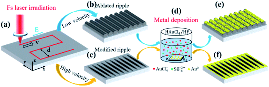
This paper aims to address the problematic aspects of such methods that complicated preparation processes and vitiated the operability of selective metal deposition and growth. In this paper, we propose a two-step method to resolve the aforementioned problems. The first preparation step comprises the fabrication of ripples with a femtosecond laser. The second preparation step is to immerse the samples in a mixed aqueous solution of HF and HAuCl4. In this step, the femtosecond laser plays a key role for the following gold-selective deposition because femtosecond laser can selectively process materials and control their properties. The proposed method may have great potential for preparing metal–semiconductor composite structures.
2. Experimental section
Materials
N-type P-hybrid single side polished silicon (100) (5 mm × 5 mm × 0.5 mm, ρ = 0.01–0.02 Ω cm), purchased from Nanjing NXNANO Tech. Co., Ltd were used. The HF solution and HAuCl4·4H2O powders purchased from Sinopharm Chemical Reagent Beijing Co., Ltd were used. The mass percentage concentration of HF is 48% to 51%. The purity of HAuCl4·4H2O is 99.95%.
Substrate fabrication
The femtosecond laser ablation of nanostructures on the silicon substrate was carried out by using a chirped-pulse Ti:sapphire laser system (Spectra Physics, Inc., Santa Clara, California, USA; 800 nm, 50 fs, 1 kHz). Before being subjected to femtosecond laser processing, the samples were ultrasonically bathed with ethanol and distilled water for 5 minutes each and were dried in a vacuum oven for 5 minutes at 40 °C. Then the samples were irradiated by a femtosecond laser. The laser pulse was perpendicularly focused on the sample surface with a 100 mm focal-length plano-convex lens. The sample was moved by a computer-controlled six-axis translation stage (HEXAPOD, PI, Inc., Karlsruhe, Germany) with a movement accuracy of 1 μm in x-axis and y-axis direction and 0.5 μm in the z-axis direction. The translating routes were Z-shaped [marked by a red dotted line in Fig. 1(a)] with different interline distances and translating speed. The ablation laser fluence was 134 mJ cm−2. After being subjected to femtosecond laser processing, the samples were ultrasonically bathed and dried as aforementioned before processing. Then, the samples were deposited in a mixed aqueous solution of 100 mM HF and 1.0 mM HAuCl4 with deposition times of 3 min and 10 min, respectively, at 25 °C. Normal indoor illumination was maintained during the reaction. The samples were immersed in distilled water to remove residual solution on the sample surfaces after the reaction.
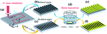 |
| | Fig. 1 Schematic of the fabrication process. First, flat silicon samples were directly irradiated by a femtosecond laser in an air atmosphere (a), thus forming ablated ripples (b) and modified ripples (c) respectively. Then, the fabricated samples were immersed in a mixed aqueous solution of HF and HAuCl4 (d) to achieve metal-selective deposition (e and f). | |
Characterization
The morphology of the fabricated samples was characterized using a scanning electron microscope (SEM S-4800) and an atomic force microscope (AFM, Dimension Edge PSS). The crystal state measurements of fabricated silicon were performed under 520 nm laser by using a Renishaw inVia Reflex spectrometer. The element composition distribution of the nanostructures was investigated through energy dispersion X-ray (EDX) spectroscopy. The X-ray photoelectron spectroscopy (XPS, ESCALAB 250Xi) was utilized to measure the chemical composition of the gold particles.
3. Results and discussion
Ripple fabrication in open air
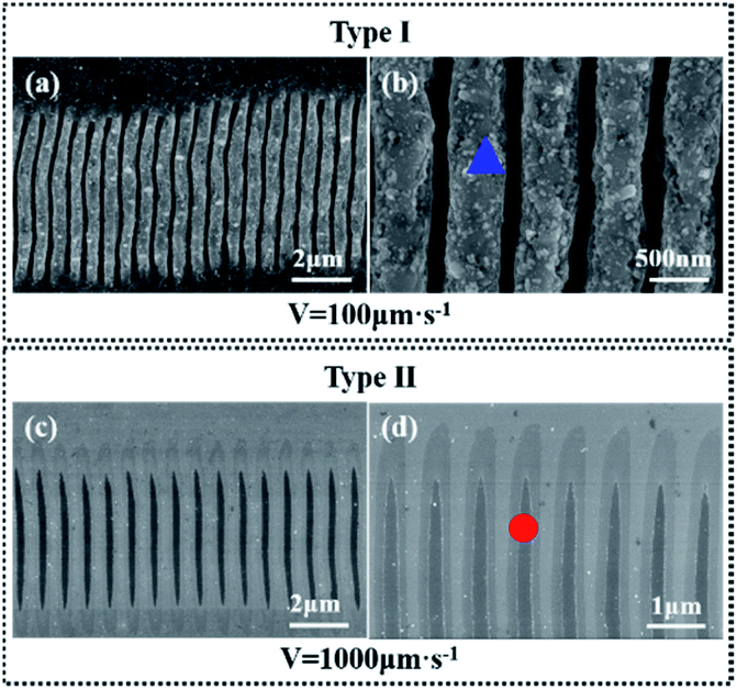
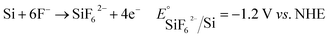
Laser ablation of silicon surfaces to make ripples has been extensively studied in recent years. Scholars have debated the exact formation mechanisms of ripples, with the most common point that incident laser light interferes with surface waves.20 The morphologies of ripples fabricated by a femtosecond laser are shown in Fig. 2. Fig. 2 Type I is an ablated ripple-processed structure on a silicon surface made by a femtosecond laser with a translating speed of 100 μm s−1; the schematic diagram is presented in Fig. 1(b). The ablated ripple can be obtained by performing a line scan with a lower translating speed for increasing number of effective pulses. Type II is a modified ripple structure processed on a silicon surface using a femtosecond laser with a translating speed of 1000 μm s−1; the schematic diagram is shown in Fig. 1(c). The modified ripple can be obtained by performing a line scan via increasing translating speed for decreasing number of effective pulses. Fig. S1† shows an AFM images of the two kinds of ripples aforementioned patterned through femtosecond laser ablation. The modified fringe height was about 14 nm and the ablated fringe height was about 250 nm and the height spatial distribution perpendicular to the fringe direction has a period of about 800 nm.
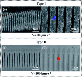 |
| | Fig. 2 Different morphologies of ripples for various translating speed. Two types exist and can be distinguished by their surface morphological and chemical characteristics: ablated ripple (Type I, (b) is a high-magnification version of (a)) and modified ripple (Type II, (d) is a high-magnification version of (c)). | |
In order to study the crystal characteristics of the different regions irradiated by femtosecond laser, the micro Raman spectroscopy experiment was carried out. Raman spectroscopy is a nondestructive, useful method for measuring the crystalline state of silicon due to amorphous silicon and monocrystals have different Raman spectra.21 Fig. 3 shows micro Raman spectra from different regions in Fig. 2 (different regions are marked by square, circle and triangle, respectively). The black line is the reference spectrum of the non-irradiated location of single crystalline (100) Si. The spectrum has a peak at 520.5 cm−1. The red line is the spectrum of the modified location and the blue line is the spectrum of the ablated location. In the two laser treated region, an additional broad band around 473 cm−1 can be seen. This is the characteristic of amorphous silicon.21 The micro Raman spectra results show that femtosecond laser irradiation produced modified nanofringes and ablated nanofringes with amorphous silicon which plays a key factor for the following selective deposition of metal ions.
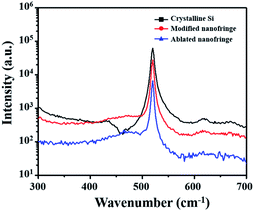 |
| | Fig. 3 Micro Raman spectra of (100) silicon surfaces. Non-irradiated surface (black line); modified nanofringe (red line); ablated nanofringe (blue line). | |
Growth of gold nanoparticles on ablated ripple of silicon surfaces via galvanic displacement
As has been mentioned, galvanic displacement has been applied in many different fields, especially in the fields related to making nanoscale metallic and semiconductor structures. Galvanic displacement does not require additional reductants, and the electrons required to reduce metal ions are provided by the substrate.12,16 During the whole process, it is necessary to ensure that the oxidized substrates can be dissolved continuously so that the electrons of the substrates can be transferred to the solution through the surface, thus promoting the continuous process of the whole reaction. In determining whether the substrate can react with metal ions and the reaction direction, it is only necessary to judge the standard electrode potentials of both.22 In the case of silicon, hydrofluoric acid must be added to ensure the continuous growth of metals, because the simultaneous formation of silicon dioxide produces a dielectric material, which prevents further reduction of metal ions. In the presence of hydrofluoric acid, the oxide layer of silicon was dissolved to soluble SiF62− in situ according to eqn (1):23| |
 | (1) |
| |
 | (2) |
In galvanic displacement research, controlling the deposition position and morphology of metals on semiconductors is a focus of research and has a crucial influence on their properties and applications. A search of the literature revealed no studies using a femtosecond laser for the regulation of metal ion reduction on silicon through galvanic displacement. Gold ions can be easily deposited on silicon in the presence of hydrofluoric acid.10 This type of reaction is suitable for the deposition of many metals on silicon surfaces. Provided that the redox potential of the metals is higher than the redox potential of silicon, theoretically, this reaction can be carried out spontaneously and metal deposition occurs.22 Therefore, a silicon sample can be ablated by a femtosecond laser and then immersed in chloroauric acid aqueous solution containing hydrofluoric acid for gold ion reduction through galvanic displacement.
The reagent concentration and deposition time are two key parameters for the selective deposition of gold particles.
Illumination is also an important parameter when deposition takes place on N-type silicon. In the absence of light, the selective deposition will be weakened, and sometimes there would be no such experimental results of selective deposition. When silicon surface is illuminated by white light, it can release electrons and generates electricity. And it has been reported that the excess electrons generated on the surface of silicon can affect the morphology of gold reduction growth.24 Therefore, in all experiments, we have guaranteed the same and appropriate natural light conditions. In this study, the chemical reaction took place in the aforementioned system shown in Fig. 1.
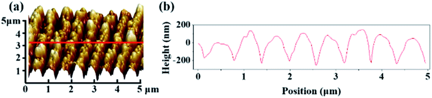
Fig. 4(a) shows an SEM image of gold particles deposited on a bare Si surface after galvanic displacement. The Si surface was fully covered with gold nanoparticles, and no selective deposition occurred. Fig. 4(b) shows the SEM image of a ripple patterned through femtosecond laser ablation and galvanic displacement. The sample was fabricated by femtosecond laser with a translating speed of 100 μm s−1. Gold particles completely covered on the protuberant part of the ripple structure; no substantial growth was observed in the recess [schematic diagram as shown in Fig. 1(e)]. The selective deposition occurred on the ablated ripple structure. Fig. 4(c) displays a high-magnification version of (b). Fig. 5(a) shows a three-dimensional AFM images of a ripple patterned through femtosecond laser ablation and galvanic displacement. Fig. 5(b) is the cross-sectional height image of (a). The height of the fringes is about 350 nm and the section shape is similar to a triangle. The EDX result in Fig. 9(a–d) presents the distribution of gold. The distribution is highly consistent with the structure. In this section we prove that a femtosecond laser can control the deposition area of gold particles on fabricated nanostructures. We speculate that the selective deposition of gold on the ablated ripple was due to the change of solute distribution on the substrate surface and it may be easier to accumulate charges on the raised position of a ripple to react with the flourishing redox reaction of gold ions.
 |
| | Fig. 4 SEM image of gold particles deposited on different silicon structures in 100 mM HF and 1.0 mM HAuCl4 mixed aqueous solution for 10 min at 25 °C through galvanic displacement. (a) SEM image of gold particles deposited on a bare Si surface. (b) SEM image of gold particles deposited on an ablated ripple of silicon. (c) A high-magnification version of (b). | |
 |
| | Fig. 5 AFM image of gold particles deposited on ablated ripple of silicon in 100 mM HF and 1.0 mM HAuCl4 mixed aqueous solution for 10 min at 25 °C through galvanic displacement. (a) AFM image. (b) Topographic AFM cross-sectional height image along the red line in panel (a). | |
Growth of gold nanoparticles on modified ripples on silicon surfaces through galvanic displacement
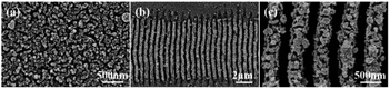
The selective deposition of gold was successfully achieved on the ablated ripple. Three-dimensional nanoscale structures may be the main reason for selective deposition. To further study gold-selective deposition by the control of a femtosecond laser, we designed a gold deposition experiment on the modified ripples. Fig. 6(a–c) shows SEM images of gold particles deposited on different morphology of ripples with galvanic displacement durations of 3 min. And Fig. 6(d) shows the deposition on bare silicon with same galvanic displacement durations. The gold deposited on the protuberant part of ablated ripple fabricated with a scanning speed of 100 μm s−1 as shown in Fig. 6(a) which was similar with the result in Fig. 4(b). With translating speed increased, ripples with ablation and modified transition state appeared in the case of a translating speed of 500 μm s−1 and gold deposition appeared on the unmodified fringes as shown in Fig. 6(b). A fully modified ripple was fabricated at a translating speed of 1000 μm s−1 and gold deposition took place on the unmodified fringes as shown in Fig. 6(c). Fig. 2(d) illustrates two places between fringes on the modified ripple; gold was deposited in a light-colored region (schematics are presented in Fig. 1(c) and (e)). A light-colored region is an unmodified region in which silicon is in a single-crystal state. The deposition growth of gold in the modified fringe region was suppressed and the nanoscale control of gold nucleation sites was realized by femtosecond laser-assisted galvanic displacement on the surface of modified planar silicon. Arrays of gold sub-micron wires formed on the surface of the silicon. The width of each sub-micron wires was approximately 300 nm, and the distance between them was approximately 480 nm. As the translating speed of the femtosecond laser increased, small amounts of gold particles appear in the modified region. The reason for this phenomenon may be that the surface of the modified ripple has different surface depressions and modification depths under different pulse numbers,25 which affects the degree of inhibition of gold deposition in the modified region. And different crystal types of ripple fringes may also be a cause of the selective deposition of gold particles on silicon substrates due to the growth of gold nanostructures on silicon through galvanic displacement is termed heteroepitaxial growth.23
 |
| | Fig. 6 SEM image of gold particles deposited on different types of ripples and bare silicon substrates through galvanic displacement events that lasted for 3 min: (a–c) ripple fabricated with translating speeds of 100, 500, 800, and 1000 μm s−1. (d) Bare silicon. | |
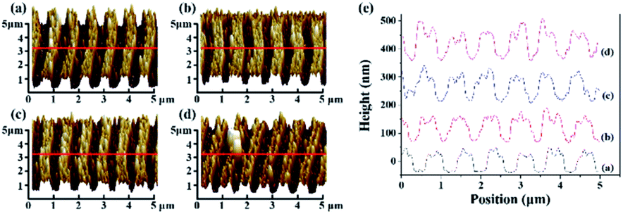
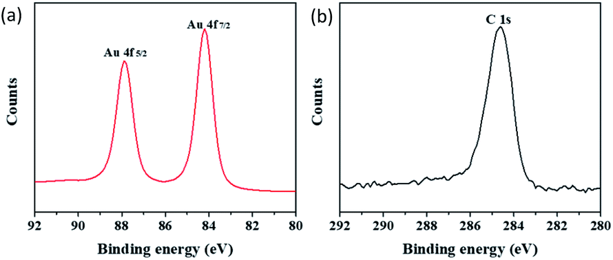
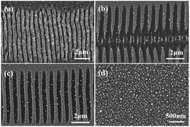
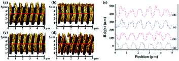
When the deposition time was increased, the modified substrate fabricated with a translating speed of 1000 μm s−1 had little effect on the gold particles selective deposition and gold particles appeared on the modified fringes as shown in Fig. 7. We measured the size of the 10 larger gold particles in the four images in Fig. 7 respectively. And made a line chart of the average diameter as shown in Fig. S4.† According to the Fig. 7 and S4,† the number and size of gold particles in the modified fringes increased with time. According to the morphology of gold particles in Fig. 7, the growth of gold is indicative of Volmer–Weber growth, which is in accordance with a previous report.23 Large-area selective deposition can be carried out using the aforementioned method (see ESI Fig. S2 and S3†) and the experiment has high repeatability. Fig. 8 shows a three-dimensional AFM images of a ripple patterned through femtosecond laser modification and galvanic displacement. Fig. 8(a–d) is the morphological evolution for different galvanic displacement reaction times of 3 min, 5 min, 8 min and 10 min and (e) is the cross-sectional height images of (a–d). The fringe height increased with time and the cross-sectional shape between fringes changed from a rectangle at 3 minutes to a triangle at 10 minutes. Fig. 9(e–h) shows the element distribution of the nanostructured gold particles deposited on modified ripples and silicon substrates after galvanic displacement; the distribution is highly consistent with the structure. Fig. 10 is an XPS test on the gold particles reduced on the ripple substrate shown in Fig. S2(c).† Fig. 10(a) is the X-ray photoelectron spectroscopy (XPS) of Au 4f spectra and Fig. 10(b) is the XPS of C 1s for charge correction spectra and C 1s binding energy region shows peak centered at 284.6 eV. The XPS spectrum in the Au 4f7/2 and Au 4f5/2 binding energy region shows peaks centered at 84.2 eV and 87.9 eV, respectively, indicating that the successful deposition of metallic gold.
 |
| | Fig. 7 Morphological evolution of gold fabricated through different galvanic displacement reaction times on modified ripples with a translating speed of 1000 μm s−1: (a) 3 min, (b) 5 min, (c) 8 min, and (d) 10 min. | |
 |
| | Fig. 8 AFM images for different galvanic duration times of gold particles deposited on modified ripples fabricated with a femtosecond laser translating speed of 1000 μm s−1: (a) 3 min, (b) 5 min, (c) 8 min, and (d) 10 min. (e) is the topographic AFM cross-sectional height image along the red line of (a–d). | |
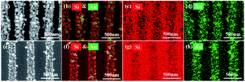 |
| | Fig. 9 EDX result of gold particles deposited on ablated ripples (a–d) and modified ripples (e–h) fabricated with translating speeds of 100 μm s−1 and 1000 μm s−1 respectively; galvanic displacement durations were 10 min and 3 min respectively. | |
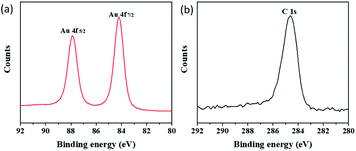 |
| | Fig. 10 XPS spectrum for Au 4f and C 1s: (a) Au 4f spectra; (b) C 1s spectra. | |
4. Conclusion
In this study, we proposed a novel, simple, mask-free galvanic displacement method to realize the selective deposition of gold particles with a femtosecond laser. The proposed method has only two simple steps. The first preparation step comprises the fabrication of ripples with a femtosecond laser. The second preparation step is to immerse the samples in a mixed aqueous solution of HF and HAuCl4. By optimizing the deposition time and solution concentration of the galvanic displacement reaction, highly ordered gold sub-micron wires can be prepared. It can be inferred from the experimental results that the width and spacing of the gold wires can be controlled by controlling the width and spacing of the ripple fringes. The essential cause of the selective deposition of metals is the selective regulation of material properties by nanoscale application of a femtosecond laser. This method is suitable for the selective deposition of any metal ions that can undergo redox with silicon under appropriate reaction conditions and has high repeatability. This method may have great application potential for preparing metal–semiconductor composite structures, including fabrication of sub-micron wires, metal-assisted semiconductor etching, energy storage, metal grating production, and other processes.
Conflicts of interest
There are no conflicts to declare.
Acknowledgements
This work was financially supported by National Key R&D Program of China (2018YFB1107200) and National Natural Science Foundation of China (51675048).
Notes and references
- S. W. Cao, Y. P. Yuan, J. Barber, S. C. J. Loo and C. Xue, Appl. Surf. Sci., 2014, 319, 344–349 CrossRef CAS
 .
. - A. Axelevitch, B. Gorenstein and G. Golan, Appl. Surf. Sci., 2014, 315, 523–526 CrossRef CAS .
- A. Gutes, I. Laboriante, C. Carraro and R. Maboudian, J. Phys. Chem. C, 2009, 113, 16939–16944 CrossRef CAS .
- Y. B. An, A. Behnam, E. Pop and A. Ural, Appl. Phys. Lett., 2013, 102, 5 Search PubMed .
- H. L. Wang, L. S. Zhang, Z. G. Chen, J. Q. Hu, S. J. Li, Z. H. Wang, J. S. Liu and X. C. Wang, Chem. Soc. Rev., 2014, 43, 5234–5244 RSC .
- Y. A. Akimov and W. S. Koh, Nanotechnology, 2010, 21, 6 CrossRef .
- H. Han, Z. P. Huang and W. Lee, Nano Today, 2014, 9, 271–304 CrossRef CAS .
- W. J. Han, E. Stepula, M. Philippi, S. Schlucker and M. Steinhart, Nanoscale, 2018, 10, 20671–20680 RSC .
- A. Lahiri, G. Pulletikurthi and F. Endres, Front. Chem., 2019, 7, 13 CrossRef .
- A. Lahiri and S. I. Kobayashi, Surf. Eng., 2016, 32, 321–337 CrossRef CAS .
- Y. Okinaka and M. Hoshino, Gold Bull., 1998, 31, 3–13 CrossRef CAS .
- L. A. Porter, H. C. Choi, A. E. Ribbe and J. M. Buriak, Nano Lett., 2002, 2, 1067–1071 CrossRef CAS .
- C. Carraro, R. Maboudian and L. Magagnin, Surf. Sci. Rep., 2007, 62, 499–525 CrossRef CAS .
- M. Cerruti, G. Doerk, G. Hernandez, C. Carraro and R. Maboudian, Langmuir, 2010, 26, 432–437 CrossRef CAS .
- Q. Wei, Y. S. Shi, K. Q. Sun and B. Q. Xu, Chem. Commun., 2016, 52, 3026–3029 RSC .
- L. Magagnin, R. Maboudian and C. Carraro, Electrochem. Solid-State Lett., 2001, 4, C5–C7 CrossRef CAS .
- S. S. Djokić, N. S. Djokić, C. Guthy and T. Thundat, Electrochim. Acta, 2013, 109, 475–481 CrossRef .
- M. Aizawa and J. M. Buriak, J. Am. Chem. Soc., 2006, 128, 5877–5886 CrossRef CAS .
- T. Soejima, Y. Katayama and S. Fujii, CrystEngComm, 2016, 18, 6683–6688 RSC .
- J. E. Sipe, J. F. Young, J. S. Preston and H. M. Vandriel, Phys. Rev. B: Condens. Matter Mater. Phys., 1983, 27, 1141–1154 CrossRef CAS .
- J. Bonse, K. W. Brzezinka and A. J. Meixner, Appl. Surf. Sci., 2004, 221, 215–230 CrossRef CAS .
- L. Magagnin, R. Maboudian and C. Carraro, J. Phys. Chem. B, 2002, 106, 401–407 CrossRef CAS .
- S. Y. Sayed, F. Wang, M. Mallac, A. Meldrum, R. F. Egerton and J. M. Buriak, ACS Nano, 2009, 3, 2809–2817 CrossRef CAS .
- A. Lahiri, R. Wen, S. Kuimalee, S.-i. Kobayashi and H. Park, CrystEngComm, 2012, 14, 1241–1246 RSC .
- D. Puerto, M. Garcia-Lechuga, J. Hernandez-Rueda, A. Garcia-Leis, S. Sanchez-Cortes, J. Solis and J. Siegel, Nanotechnology, 2016, 27, 8 CrossRef .
Footnote |
| † Electronic supplementary information (ESI) available. See DOI: 10.1039/d0ra03059g |
|
| This journal is © The Royal Society of Chemistry 2020 |
Click here to see how this site uses Cookies. View our privacy policy here. 
 Open Access Article
 This Open Access Article is licensed under a Creative Commons Attribution-Non Commercial 3.0 Unported Licence
 ,
Jie Hu
,
Jie Hu