
 Open Access Article
 This Open Access Article is licensed under a Creative Commons Attribution-Non Commercial 3.0 Unported Licence
An efficient and stable inverted perovskite solar cell involving inorganic charge transport layers without a high temperature procedure
Jien Yang *ab,
Jinjin Xua,
Qiong Zhanga,
Zhilin Xueb,
Hairui Liub,
Ruiping Qinb,
Haifa Zhaib and
Mingjian Yuanc
*ab,
Jinjin Xua,
Qiong Zhanga,
Zhilin Xueb,
Hairui Liub,
Ruiping Qinb,
Haifa Zhaib and
Mingjian Yuanc
aHenan Key Laboratory of Photovoltaic Materials, School of Physics, Henan Normal University, Xinxiang, China. E-mail: yjen@htu.edu.cn
bSchool of Materials Science and Engineering, Henan Normal University, Xinxiang 453007, China
cCollege of Chemistry, Nankai University, Tianjin 300071, China
First published on 18th May 2020
Abstract
Despite the successful enhancement in the high-power conversion efficiency (PCE) of perovskite solar cells (PSCs), the poor stability of PSCs is one of the major issues preventing their commercialization. The attenuation of PSCs may be due to the lower heat resistance of the organic charge transport layer and the tendency to aggregate at high temperatures. Here we report cerium oxide (CeOx) as an electron transport layer (ETL) prepared through a simple solution processed at a low temperature (∼100 °C) to replace the organic charge transport layer on top of the inverted planar PSCs. The CeOx layer has excellent charge selectivity and can provide the perovskite film with protection against moisture and metal reactions with the electrode. The solar cell with CeOx as the electron transport layer has a power conversion efficiency of 17.47%. These results may prove a prospect for practical applications.
Introduction
The organic–inorganic metal halide perovskite solar cells (PSCs) have undergone rapid development and attracted extensive attention, with a power conversion efficiency (PCE) increasing from 3.8% up to the latest certified efficiency of 25.2% within 10 years.1–7 The soaring of PCE has been achieved by various methods, such as compositional modification; improvement on the quality of the perovskite film, and the development of highly efficient electron transport layers (ETLs).8–10 Although the PCE has been enhanced, the poor stability of PSCs has prevented their commercialization. The poor stability of the PSCs may be due to the instability of the weakly bonded organic–inorganic perovskite materials,8,9 and the degradation of their external layers, interfaces and device structure.10In an inverted planar structure, there are several materials used as electron transport layers, such as PCBM,11–13 fullerene derivatives,14 polyelectrolyte15,16 and other organic semiconductors. Among them, PCBM and fullerene derivatives are widely used because they have energy levels suitable for solar cells. However, these molecules will aggregate after high annealing temperatures during the fabrication.17 This situation will influence the stability of the PSCs' interface and pin-holes will easily form decreasing the performance of the device. On the other hand, these organic transport materials usually require complicated syntheses and purification processes, which will increase the whole cost.18,19 Therefore, the inorganic ETLs have attracted extensive attention to improve the stability and decrease the cost of PSCs.
Among these inorganic electron transport materials, cerium oxide (CeOx) has been applied in PSCs in different roles. CeOx are considered one of the most earth abundant rare-earth metal oxides, implying their potential for the low cost production of these devices.20 It is an n-type semiconductor with a wide bandgap, resulting in a low absorption loss and high value band edge resulting coincidentally in efficient hole-blocking. Besides, this material has outstanding electrical properties such as high ionic conductivity and high electron mobility.21 More importantly, CeOx have high thermal and chemical stability,22 which can replace common organic electron transport materials in the storage and release of oxygen. Because of its excellent properties, CeOx are promising materials with application in various areas, such as catalysis,23 electrochemical displays,24 high temperature ceramics, and UV blocking materials.25,26 In this study, we demonstrate that solution processed CeOx can be easily prepared using a simple sol–gel method at a low temperature, and applied as the ETL in an inverted planar PSC to increase its efficiency and enhance the stability. Finally, the inverted type device ITO/NiOx/CH3NH3PbI3/CeOx/Ag exhibits the best PCE of 17.47% and retains 85% of the initial efficiency for 300 h, which is significantly better compared to the PCBM device.
Results and discussion
In our study, the CeOx thin film replaces the PCBM to be used as the ETL in the inverted planar PSC. To the best of our knowledge, a suitable energy level is important for the ETL in PSCs, which can efficiently transport the electrons and block the holes. The optical bandgap of CeOx can be obtained from the UV-vis absorbance spectrometry (Fig. 1b). The direct bandgap energy (Eg) for the CeOx thin film is determined by the direct transition equation,27 (αhν)2 = A(hν − Eg), where α is the absorption coefficient, A is a constant and Eg is the direct bandgap. The plot of (αhν)2 versus hν is shown in the inset of Fig. 1b, and Eg of the CeOx thin film was determined to be 3.5 eV. Ultraviolet photoelectron spectroscopy (UPS) of the CeOx film is shown in Fig. 1c. The highest occupied molecular orbital (HOMO) energy level is determined using equation,28 EHOMO = hν − (EHOMOonset − Ecutoff), where hν is the incident photon energy and the Ecutoff is the lowest kinetic measured energy of the electrons. The EHOMOonset is the HOMO energy onset, which is defined as the highest kinetic energy onset. The HOMO of the CeOx film is 7.5 eV. The lowest unoccupied molecular orbital (LUMO) energy level can be calculated through the optical bandgap and the HOMO energy level. The LUMO of the CeOx film is 4.0 eV, which is slightly lower than the LUMO for CH3NH3PbI3 and shows a better energy level alignment with CH3NH3PbI3 than that used in PCBM ETL. The corresponding energy level diagram of the device is shown in Fig. 1a. It implies that the CeOx film has an effective ability to transport electrons and block the holes.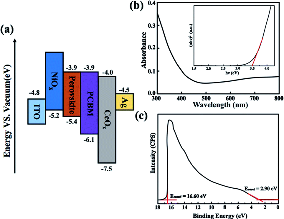 | ||
| Fig. 1 (a) Energy band diagram of the components in the device. (b) UV-vis absorption spectra of the CeOx film. (The inset shows the plots of the (αhν)2 versus energy) (c) UPS spectra of the CeOx film. | ||
In order to investigate the composition of the CeOx film, X-ray photoelectron spectroscopy (XPS) measurement is carried out (Fig. 2). The Ce 3d spectrum can be assigned to the two sets of spin–orbital multiples, 3d3/2 and 3d5/2, labeled as u and v, respectively.29,30 For the valence +4 of cerium, a mixture of Ce3d94f2O2p4, Ce3d94f1O2p5 and Ce3d94f0O2p6 is labeled as u, u′′, u′′ and v, respectively, and v′′, v′′′ for Ce 3d3/2 and Ce 3d5/2, respectively. For the valence +3 of cerium, the peaks v0, v′ and u0, u′ are assigned to a mixture of Ce3d94f2O2p5 and Ce3d94f0O2p6, respectively.31,32 The Ce 3d spectrum of CeO2 shows six peaks at 916.4(u′′′), 905.7(u′′), 900.6(u), 897.7(v′′′), 887.6(v′′) and 882.4(v). These peaks represent the presence of Ce4+. In addition, Ce3+ has four peaks at 903.2(u′), 898.6(u0), 885.2(v′) and 881.1(v0). The concentrations of Ce3+ can be calculated using the equation 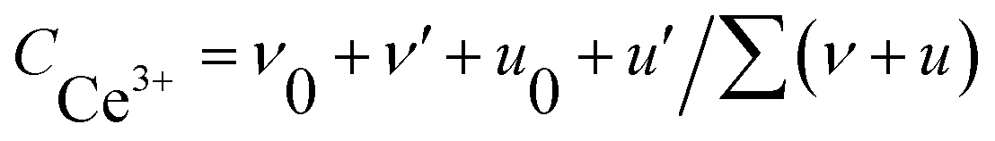 . According to the intensity of the ν0, ν′, u0 and u′, the concentrations of Ce3+ in the Ce 3d spectrum is 0.44, so the x of the CeOx is 1.78.
 | ||
| Fig. 2 XPS spectra for the decomposition of the Ce 3d core level into the emissions of Ce4+ and Ce3+. | ||
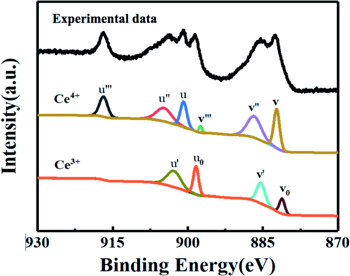
In order to testify the suitability of the CeOx film as the ETL in PSCs, some optical and electrical properties have been tested. To investigate the charge transfer dynamics, steady-state and time-resolved photoluminescence (PL) measurements have been performed. The steady-state PL quenching demonstrates that the charge transfer is more efficient after the use of the CeOx film as ETL, as shown in Fig. 3a. It can be seen that all of the samples show luminescence peaks centered at 768 nm. However, a prominent decrease in the PL peak intensity can be found in CeOx. The decreased PL intensity indicates that CeOx has stronger interfacial electron extraction efficiency.33,34 Moreover, the time-resolved PL (TRPL) decay is fitted with a bi-exponential decay function (Fig. 3b). The faster decay component (τ1) is attributed to charge carrier trapping defect states, while the slower one (τ2) is due to the radiative recombination in the bulk crystals.35 With the use of CeOx, the faster decay component (30 ns) is reduced compared to that of the pristine perovskite film (74 ns), which indicates that the CeOx film can reduce the defect density in the perovskite. Furthermore, the τ2 decreases from 198 ns (perovskite) to 129 ns (perovskite/CeOx), indicating that CeOx has a more efficient charge transport. As a result, the CeOx can reduce the charge carrier trapping, speed up electron extraction and enhance the performance of the PSC device.
 | ||
| Fig. 3 (a) Steady PL spectra. (b) Time-resolved PL spectra. | ||
Beside this, the space-charge-limited current (SCLC) measurement has been tested to confirm the electron extraction and the defect density of the CeOx ETL in the PSC. The structure of the pure electronic device is shown in Fig. 4a. As shown in Fig. 4b, the trap-state density for CeOx devices can be determined by the trap-filled limit voltage in the equation Ntrap = 2ε0εrVTFL/eL2,36,37 and calculated to be 31.52 × 1015 cm−3, which is much lower than that of the reference devices (39.89 × 1015 cm−3). It indicate5.s that CeOx as ETL can reduce the trap density compared with the PCBM-based device. We further calculated the charge carrier mobility using the equation J = 9ε0εrμV/8L2, where μ is the charge mobility and V is the applied voltage. The mobility also was enhanced from 1.16 × 10⁻² cm2 V−1 s−1 ns (reference devices) to 5.52 × 10⁻² cm2 V−1 s−1 (CeOx device).38 This result demonstrates that the device with CeOx exhibits a more efficient electron extraction from the perovskite layer.
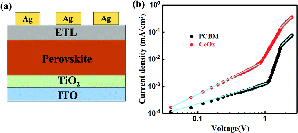 | ||
| Fig. 4 (a) Schematic of the pure electronic layer device structure. (b) SCLC plots of Ag/ETL/perovskite/TiO2/ITO devices. | ||
In order to confirm the validity of the use of CeOx as ETL in enabling high performance PSCs, the J–V curves of the champion devices have been tested (Fig. 5a) and the corresponding common performance parameters such as open-circuit (Voc), short-circuit current density (Jsc), fill factor (FF), and PCE are illustrated in Table 1. The reference device yields similar PCEs of 14.28% under forward scan (FS) and 15.33% under reverse scan (RS). In comparison, the CeOx device achieves a much-enhanced PCE of 16.61% with a Voc of 1.01 V, a Jsc of 22.35 mA cm−2, and an FF of 73.59 under FS, and a PCE of 17.47% with a Voc of 1.03 V, a Jsc of 22.51 mA cm−2, and an FF of 75.36 under RS. Beside this, the statistics of the PCEs for 24 independent devices fabricated with the reference devices and the devices using CeOx as the ETL. As presented in Fig. 5b, both devices have a similar distribution, implying that the perovskite device is reproducible, no matter whether PCBM or CeOx film have been used as the ETL. The average PCE is calculated to be 14.51% for the reference devices. Encouragingly, the average PCE has been enhanced to 16.89% for the ones fabricated with CeOx. The inferior PCE may be due to the degeneration of the perovskite layer by water through the PCBM ETL. Noting that all of the devices have shown a similar J–V hysteresis phenomenon. Further, the time-dependent PCE outputs of these devices without encapsulation are recorded at ambient conditions and the devices are biased at their respective maximum power points. As show, in Fig. 5c, the stabilized efficiency output is estimated to be 16.89% for the solar cell with CeOx as ETL after being measured over 300 s, which is much higher than that of the PCBM as ETL. This fact can give evidence of the superior stability of the CeOx at ambient conditions compared to the PCBM.
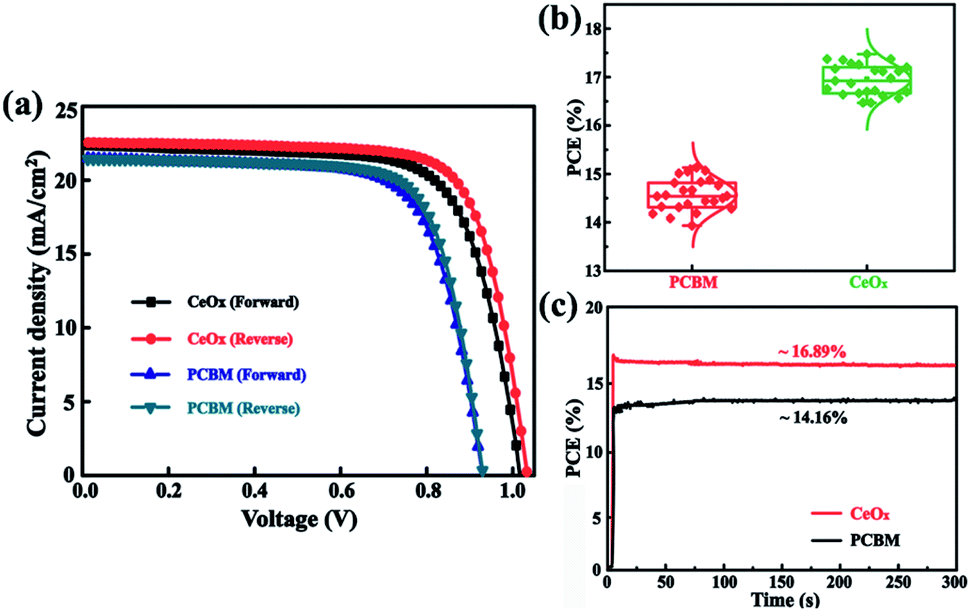 | ||
| Fig. 5 (a) J–V curves of the perovskite solar cells based on different ETLs measured in different scan directions. (b) Statistic distributions of PCEs for 24 independent cells fabricated with different ETLs. (c) Steady-state maximum PCE outputs. | ||
| ETL | J/V sweep direction | Voc (V) | Jsc (mA cm−2) | FF (%) | PCE (%) |
|---|---|---|---|---|---|
| PCBM | Forward | 0.93 | 21.49 | 71.47 | 14.28 |
| Reverse | 0.94 | 21.43 | 74.53 | 15.02 | |
| CeOx | Forward | 1.01 | 22.35 | 73.59 | 16.61 |
| Reverse | 1.03 | 22.51 | 75.36 | 17.47 |
The external quantum efficiency (EQE) spectrum of the devices was measured and is shown in Fig. 6a. The device with CeOx as ETL exhibits a higher EQE because the CeOx film has a more efficient light trapping ability than the PCBM film. The corresponding integrated Jsc of these devices based on the CeOx and PCBM ETLs is 20.94 and 18.05 mA cm−2, respectively. This result indicates that the device based on the CeOx has a better photoelectric conversion property.
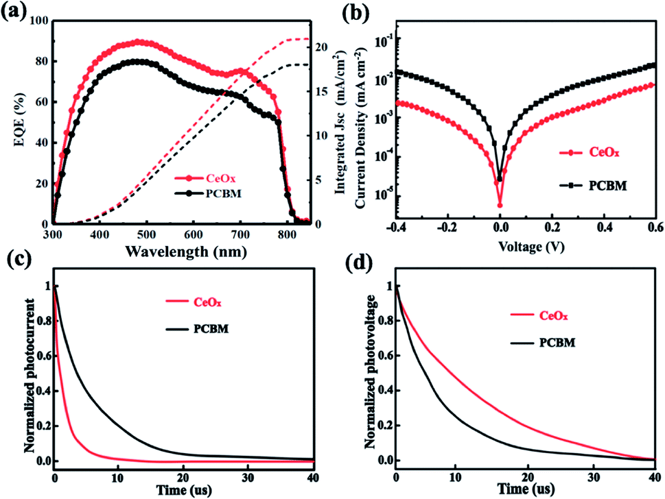 | ||
| Fig. 6 (a) EQE spectra. (b) Dark J–V curves plotted on a semi-log scale. (c) TPC decay curves. (d) TPV decay curves. | ||
To study the difference between the photovoltaic properties of the two champion devices, the dark current has been measured (Fig. 6b). It can be seen that the device with CeOx exhibits a smaller leak current under low bias voltages and dark current under high bias voltages, which effectively increases the Voc.39,40 As expected, the device with CeOx improves the current injection and prevents the current leakage under low voltages. Furthermore, the transient photovoltage (TPV) and transient photocurrent (TPC) are performed to investigate the carrier transfer and recombination properties of these devices. It can reflect the transport and extraction properties of the carrier, and supply the carrier recombination in PSCs.41–43 As drawn from Fig. 6c, the slower photovoltage decay of the device based on CeOx in comparison to the one of the reference device, indicates that the recombination of carriers can be suppressed with CeOx. Simultaneously, as showed in Fig. 6d, the device based on CeOx delivers faster photocurrent decays in comparison to the reference device, conveying that the transport and extraction of carriers are more efficient after the use of CeOx as ETL. These results demonstrate that the device fabricated with CeOx has better dynamic features of carriers, further improving the cell performance.
Finally, the stability of the devices was further examined. Fig. 7a shows the time-dependent variation of the normalized PCE for these devices stored at 30 °C in ambient air with the humidity of 50%. It is clearly seen that the cell could retain 85% of its initial efficiency after being stored for 300 h. However, the device performance based on PCBM was reduced to 70% after 300 h. The degradation of the perovskite may be caused by water when these devices are exposed to air. In order to further study the importance of CeOx in the process, aged cells have been tested. The devices of different ETLs have been exposed to ambient air for 24 h. It can be seen from Fig. 7b and c that there are many pinholes appearing on the Ag film of the device based on PCBM, but no significant change in morphology is observed for the device based on CeOx. This situation is mainly due to the fact that organic ETLs are not dense enough to prevent the contact of the perovskite with water and isolate the perovskite layer from the Ag electrode. The schematic of Fig. 7d and e reflects the characteristics of the two films. This result demonstrates that CeOx not only have effective long-time stability against humidity but also can prevent the corrosion of the Ag electrode. Overall, the inverted planar PSCs based on CeOx possess an effective long-term protection against humidity, which gives a great prospect for practical applications.
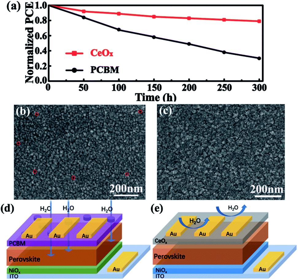 | ||
| Fig. 7 (a) Normalized efficiency decay of perovskite solar cells with different ETLs. (b) SEM of the Ag film on the PCBM and (c) on the CeOx layers. (d) Schemes of the ageing of the PCBM and (e) CeOx samples. | ||
Experimental
Materials
Nickel(II) nitrate hexahydrate (Ni(NO3)2·6H2O, 98.5%), cerium(III) acetylacetonate hydrate (Ce(C5H7O2)3·xH2O) and sodium hydroxide (NaOH, anhydrous, 98%) were purchased from Aladdin. Reagent (Shanghai) Co., Ltd. Dimethyl sulfoxide (DMSO, anhydrous, 99.7%), N,N-dimethylformamide (DMF, anhydrous, 99.8%) and chlorobenzene (C6H5Cl, anhydrous, 99.8%) were purchased from Sigma-Aldrich. Methylammonium iodide (CH3NH3I, 99.5%) and lead diiodide (PbI2, 99.99%) were purchased from Xinxiang Orderchemistry New Material Co., Ltd. All chemicals were used without further purification.Device fabrication
Indium tin oxide (ITO) glass is sequentially cleaned with detergent, deionized water, acetone and alcohol under sonication. Then, dried with a N2 flow and finally treated under oxygen plasma. To prepare the NiOx solution, 0.5 mol of nickel(II) nitrate hexahydrate was dissolved in 100 mL of deionized water and stirred at room temperature. Then, a solution of 10 mol L−1 of sodium hydroxide was added until the pH value reached 10. After stirring for several minutes, a green precipitate was collected by centrifugation and washed two times with deionized. The obtained green precipitate was dried at 80 °C for 6 hours and calcined for 2 hours at 270 °C. After dissolving the NiOx power in water, a NiOx hole transport layer is spin-coated on the ITO glass at 1500 rpm for 1 min. The perovskite precursor solution is prepared by adding 223 mg of CH3NH3I and 645 mg of PbI2 into DMF and DMSO (4![[thin space (1/6-em)]](https://www.rsc.org/images/entities/char_2009.gif) :1 volume ratio), and stirred at 60 °C for 2 h. The CH3NH3PbI3 perovskite film is applied by spin coating at 5000 rpm for 10 s, and annealed at 100 °C for 10 min. The CeOx precursor solution was obtained by dissolving cerium(III) acetylacetonate hydrate in chlorobenzene at different concentrations, followed by ultrasonication for 30 min. Then, a CeOx ETL is formed through spin coating on top of the perovskite film at 2000 rpm for 30 s and annealed under N2 at 100 °C for 10 min. Finally, a 100 nm Ag electrode is deposited on top of the CeOx layers using thermal evaporation under a base pressure of 5 × 10⁻⁴ Pa.
:1 volume ratio), and stirred at 60 °C for 2 h. The CH3NH3PbI3 perovskite film is applied by spin coating at 5000 rpm for 10 s, and annealed at 100 °C for 10 min. The CeOx precursor solution was obtained by dissolving cerium(III) acetylacetonate hydrate in chlorobenzene at different concentrations, followed by ultrasonication for 30 min. Then, a CeOx ETL is formed through spin coating on top of the perovskite film at 2000 rpm for 30 s and annealed under N2 at 100 °C for 10 min. Finally, a 100 nm Ag electrode is deposited on top of the CeOx layers using thermal evaporation under a base pressure of 5 × 10⁻⁴ Pa.
Characterization
The surface morphology of the perovskite film and section morphology of the PSC was characterized using a field emission scanning electron microscope (FESEM, Quanta 200 FEG, FEI Co.). The time-resolved (PL) spectra were acquired using a FLS920 spectrometer from Edinburgh Instruments. The current density–voltage (J–V) curves were measured (2400 Series Source Meter, Keithley Instruments) under simulated air mass 1.5 global sunlight (AM 1.5G). The external quantum efficiency (EQE) measurement was performed through a combination system of xenon lamp, monochromator, chopper and lock-in amplifier together with a calibrated silicon photodetector. UV-Vis absorption measurements of the CeOx film were carried out in a Shimadzu UV-2550 spectrometer. The X-ray photoelectron spectroscopy (XPS) measurement was performed using an AXIS Ultra instrument (Kratos UK) at a base pressure of ∼10–8 torr at 295 K.Conclusions
In summary, cost-effective and efficient inverted planar PSCs are demonstrated with a metal oxide film by a solution-processed ETL. The CeOx film on the top of the perovskite layer can prevent the system from interacting with water and retard its degradation. Moreover, the CeOx film can increase the electron extraction due to the suitable energy alignment with the perovskite. Hence, a high-quality PSC yields the optimized PCE of 17.47% and maintains 85% of its original PCE after storage in ambient conditions for 300 h. The outstanding performance of this device is mainly attributed to CeOx, which not only decreases the recombination loss and enhances the electron extraction ability, but also protects the perovskite against water to prolong its life-span. In addition, our study may promote further research and can be applied to other perovskite solar cells.Conflicts of interest
There are no conflicts to declare.Acknowledgements
This research was funded by the National Nature Science Foundation of China (No. 21402042), Tackling Key Scientific and Technological Problems of the Henan Province (No. 192102210173).Notes and references
- K. Akihiro, T. Kenjiro, S. Yasuo and M. Tsutomu, J. Am. Chem. Soc., 2009, 131, 6050–6051 CrossRef PubMed.
- Z. Huanping, C. Qi, L. Gang, L. Song, S. Tze-Bing, D. Hsin-Sheng, H. Ziruo, Y. Jingbi, L. Yongsheng and Y. Yang, Science, 2014, 345, 542–546 CrossRef PubMed.
- Q. Dong, Y. Fang, Y. Shao, P. Mulligan, J. Qiu, L. Cao and J. Huang, Science, 2015, 347, 967–970 CrossRef CAS PubMed.
- W. S. Yang, B. W. Park, E. H. Jung, N. J. Jeon, Y. C. Kim, D. U. Lee, S. S. Shin, J. Seo, E. K. Kim and J. H. Noh, Science, 2017, 356, 1376–1379 CrossRef CAS PubMed.
- Y. Jiang, J. Yuan, Y. Ni, J. Yang, Y. Wang, T. Jiu, M. Yuan and J. J. J. Chen, Joule, 2018, 2, 1356–1368 CrossRef.
- L. Wang, Y. Xue, M. Cui, Y. Huang, H. Xu, C. Qin, J. Yang, H. Dai and M. J. A. C. Yuan, Angew. Chem., Int. Ed., 2020, 132, 6504–6512 CrossRef.
- J. Yang, S. Chen, J. Xu, Q. Zhang, H. Liu, Z. Liu and M. J. A. S. Yuan, Appl. Sci., 2019, 9, 4393 CrossRef CAS.
- H. S. Kim, J. Y. Seo and N. G. Park, Chemsuschem, 2016, 9, 2528–2540 CrossRef CAS PubMed.
- A. Walsh, J. Phys. Chem. C, 2015, 119, 5755 CrossRef CAS PubMed.
- D. Wang, M. Wright, N. K. Elumalai and A. Uddin, Sol. Energy Mater. Sol. Cells, 2016, 147, 255–275 CrossRef CAS.
- A. Mingorance, H. Xie, H. S. Kim, Z. Wang, M. Balsells, A. Morales-Melgares, N. Domingo, N. Kazuteru, W. Tress and J. Fraxedas, Adv. Mater. Interfaces, 2018, 5, 1800367 CrossRef.
- T. Niu, J. Lu, R. Munir, J. Li, D. Barrit, X. Zhang, H. Hu, Z. Yang, A. Amassian and K. Zhao, Adv. Mater., 2018, 30, 1706576 CrossRef PubMed.
- T. He, Z. Liu, K. Liu, J. Wang, Y. Zhou, J. Yang, H. Liu, Y. Jiang, H. Ma and M. Yuan, J. Mater. Chem. A, 2017, 5, 24282–24291 RSC.
- B. Yang, X. Meng and S. Yang, Adv. Energy Mater., 2017, 8, 1701883 Search PubMed.
- L. Zhang, X. Zhou, X. Zhong, C. Cheng, Y. Tian and B. Xu, Nano Energy, 2019, 57, 248–255 CrossRef CAS.
- B. R. Lee, J. C. Yu, J. H. Park, S. Lee, C.-K. Mai, B. Zhao, M. S. Wong, E. D. Jung, Y. S. Nam and S. Y. Park, ACS Nano, 2018, 12, 5826–5833 CrossRef CAS PubMed.
- T. Hu, S. Xiao, H. Yang, L. Chen and Y. Chen, Chem. Commun., 2018, 54, 471–474 RSC.
- Z. Fei, C. Yi, W. Peng, X. Bi, J. Luo, G. Jacopin, S. Wang, X. Li, X. Yin and S. M. Zakeeruddin, Adv. Energy Mater., 2016, 6, 1600461 CrossRef.
- R. Fang, S. Wu, W. Chen, Z. Liu, S. Zhang, R. Chen, Y. Yue, L. L. Deng, Y. Cheng and L. Han, ACS Nano, 2018, 12, 2403–2414 CrossRef CAS PubMed.
- J. Yang, Q. Zhang, J. Xu, H. Liu, R. Qin, H. Zhai, S. Chen and M. J. N. Yuan, Nanomaterials, 2019, 9, 1666 CrossRef CAS PubMed.
- X. Wang, L.-L. Deng, L.-Y. Wang, S.-M. Dai, Z. Xing, X.-X. Zhan, X.-Z. Lu, S.-Y. Xie, R.-B. Huang and L.-S. Zheng, J. Mater. Chem. A, 2017, 5, 1706–1712 RSC.
- Z. Huan-Ping, W. Hao-Shuai, S. Jie, Y. An-Xiang, S. Ling-Dong and Y. Chun-Hua, J. Am. Chem. Soc., 2010, 132, 4998–4999 CrossRef PubMed.
- C. T. Campbell and C. H. F. Peden, Science, 2005, 309, 713–714 CrossRef CAS PubMed.
- D. Camino, D. Deroo, J. Salardenne and N. Treuil, Sol. Energy Mater. Sol. Cells, 1995, 39, 349–366 CrossRef CAS.
- T. Masui, K. Fujiwara, K. I. Machida and G. Y. Adachi, Chem. Mater., 1997, 9, 2197–2204 CrossRef CAS.
- T. Masui, M. Yamamoto, T. Sakata, H. Mori and G. Y. Adachi, J. Mater. Chem., 2000, 10, 353–357 RSC.
- K. Woo, Y. Kim and J. Moon, Energy Environ. Sci., 2012, 5, 5340 RSC.
- Y. Liu, Z. Liu and E.-C. Lee, ACS Appl. Energy Mater., 2019, 2, 1932–1942 CrossRef CAS.
- P. Burroughs, A. Hamnett, A. F. Orchard and G. Thornton, J. Chem. Soc., Dalton Trans., 1976, 17, 1686–1698 RSC.
- A. Pfau and K. D. Schierbaum, Surf. Sci., 1994, 321, 71–80 CrossRef CAS.
- B. M. Reddy, A. Khan, Y. Yamada, T. Kobayashi, S. Loridant and J. C. Volta, Langmuir, 2003, 19, 3025–3030 CrossRef CAS.
- Z. A. Tan, L. Li, L. Cong, Y. Li, F. Wang, X. Jia, Y. Lu, S. Bo, J. Hou and Y. Li, Adv. Mater. Interfaces, 2014, 1, 1400197 CrossRef.
- B. Yang, H. Chen, X. Shuang, Q. Xue, Z. Teng, Z. Zhu, L. Qiang, H. Chen, Y. Yun and Z. Hu, Adv. Funct. Mater., 2016, 26, 2950–2958 CrossRef.
- Z. Liu, A. Zhu, F. Cai, L. Tao, Y. Zhou, Z. Zhao, C. Qi, Y. B. Cheng and H. Zhou, J. Mater. Chem. A, 2017, 5, 6597–6605 RSC.
- Y. Dong, Z. Xin, R. Yang, Y. Zhou, Y. Wei, X. Wang, C. Li, S. F. Liu and R. Chang, Energy Environ. Sci., 2016, 9, 3071–3078 RSC.
- S.-C. Yun, S. Ma, H.-C. Kwon, K. Kim, G. Jang, H. Yang and J. Moon, Nano Energy, 2019, 59, 481–491 CrossRef CAS.
- C. Shen, Y. Wu, H. Zhang, E. Li, W. Zhang, X. Xu, W. Wu, H. Tian and W.-H. Zhu, Angew. Chem., Int. Ed., 2019, 58, 3784–3789 CrossRef CAS PubMed.
- R. Cheng, C. C. Chung, H. Zhang, Z. Zhou, P. Zhai, Y. T. Huang, H. Lee and S. P. J. S. Feng, Small, 2019, 15, 1804465 CrossRef PubMed.
- J. Shi, J. Dong, S. Lv, Y. Xu, L. Zhu, J. Xiao, X. Xu, H. Wu, D. Li, Y. Luo and Q. Meng, Appl. Phys. Lett., 2014, 104, 063901 CrossRef.
- W. Zhu, Q. Zhang, D. Chen, Z. Zhang, Z. Lin, J. Chang, J. Zhang, C. Zhang and Y. J. A. E. M. Hao, Adv. Energy Mater., 2018, 8, 1802080 CrossRef.
- L. Jiang, J. Lu, S. R. Raga, J. Sun, X. Lin, W. Huang, F. Huang, U. Bach and Y.-B. J. N. E. Cheng, Nano Energy, 2019, 58, 687–694 CrossRef CAS.
- H. Dong, Z. Wu, J. Xi, X. Xu, L. Zuo, T. Lei, X. Zhao, L. Zhang, X. Hou and A. K.-Y. Jen, Adv. Funct. Mater., 2018, 28, 1704836 CrossRef.
- C. Zhu, X. Niu, Y. Fu, N. Li, C. Hu, Y. Chen, X. He, G. Na, P. Liu and H. J. N. c. Zai, Nat. Commun., 2019, 10, 1–11 CrossRef PubMed.
| This journal is © The Royal Society of Chemistry 2020 |