
 Open Access Article
 This Open Access Article is licensed under a Creative Commons Attribution-Non Commercial 3.0 Unported Licence
Effect of thiophene linker addition to fluorene-benzotriazole polymers with the purpose of achieving white emission in OLEDs†
Cansu Kokab,
Ceylan Doyranlib,
Betül Canımkurbey cd,
Selin Pıravadılı Mucur*e and
Sermet Koyuncu*af
cd,
Selin Pıravadılı Mucur*e and
Sermet Koyuncu*af
aDepartment of Energy Resources and Management, Çanakkale Onsekiz Mart University, 17020 Çanakkale, Turkey
bDepartment of Chemistry, Faculty of Arts and Sciences, Yıldız Technical University, 34220 Istanbul, Turkey
cS. Şerefeddin Health Services Vocational School, Amasya University, Amasya, 05100, Turkey
dCentral Research Laboratory, Amasya University, 05100, Amasya, Turkey
eMaterials Institute, Marmara Research Center (MAM), The Scientific and Technological Research Council of Turkey (TUBITAK), 41470, Gebze, Kocaeli, Turkey. E-mail: selin.piravadili@tubitak.gov.tr
fDepartment of Chemical Engineering, Faculty of Engineering, Canakkale Onsekiz Mart University, 17100 Canakkale, Turkey. E-mail: skoyuncu@comu.edu.tr
First published on 15th May 2020
Abstract
With the purpose of obtaining white emission from single layer organic light emitting diodes (OLEDs), fluorene benzotriazole based polymers with double bond subunits (namely TP2 and SP3 with and without thiophene linker, respectively) were synthesized by a Suzuki cross-coupling polymerization reaction. SP3 and TP2 were used as an emissive layer of the OLED devices due to their outstanding solubility in organic solvents, photoluminescence intensity and morphological suitability for fine thin film-forming capability. The optical, electrochemical, light emission and electroluminescence characteristics, Density Functional Theory (DFT) calculations and admittance spectroscopic analysis of OLEDs based on SP3 and TP2 were realized in detail to understand the effects of thiophene linker addition as a donor unit to the main chain of fluorene benzotriazole based polymers. As a result, TP2 emitted a bright yellow emission with a maximum brightness of 243 cd m−2 at 40 mA cm−2, and a maximum current efficiency of 1.38 cd A−1 with more broad electroluminescence characteristics than SP3 polymer without the thiophene linker. SP3 emitted a greenish yellow emission with a maximum brightness of 1001 cd m−2 at 845 mA cm−2, and a maximum current efficiency of 0.33 cd A−1. Carrier transport properties, charge carrier transit time and the equivalent circuit modelling studies were obtained through admittance spectroscopy. An equivalent circuit model with a combination of two resistors and one capacitor explained the charge conduction mechanism of SP3 and TP2 based OLEDs. SP3 and TP2 OLED devices represented typical p-type transporting characteristics with mobilities of 0.073 and 0.017 cm2 V−1 s−1, respectively with simplified device configuration. All the results indicate that thiophene addition to the main chain of fluorene benzotriazole based polymers with double bond subunits lead to a promising candidate for white emissive materials used in single layer white OLEDs.
1 Introduction
Research about optoelectronic characteristics of π-conjugated polymers started with the synthesis of polyacetylene1 and has continued since the 1970s. Chiang et al. doped these polymers to obtain conducting polymers.2 In 1990, a pioneering study was carried out by Burroughes et al. about polymer based organic light emitting diodes (OLEDs). The synthesis and electroluminescence (EL) of the poly-phenylene vinylene (PPV)3 specified the polymer optoelectronic field. Thereafter, Heeger, MacDiarmid and Shirakawa were awarded the Chemistry Nobel prize in 2000 due to the discovery and development of conductive polymers.4 The optical and electrochemical properties of conductive polymers with their conjugated structure could reveal their intrinsic electronic characteristics. Thus, they are notably desirable materials for the optoelectronics area. They have been studied for their superior potentials in countless device applications such as, electrochromic smart windows (ECDs),5 organic light emitting diodes (OLEDs),6 organic photovoltaic devices (OPVs)7 and thin film transistors (OFETs). Functionality of their molecular structure make researchers eligible to synthesize new molecules with improved electrical and optical properties based on optoelectronic devices.In the light of this information, we went towards in donor–acceptor units to synthesize low bandgap copolymers with high performance to achieve white emission in the OLED applications. Recently, researcher has worked for obtaining suitable materials to get efficient white OLEDs. With their high efficiency, color-tunability, and color-quality, white OLEDs are emerging to become one of the next generation light sources.8 The benzothiadiazole (BT) unit is a common and well-used as electron acceptor layer. It has a nitrogen-containing heterocyclic benzazole derivative and electron-attracting imine (–C![[double bond, length as m-dash]](https://www.rsc.org/images/entities/char_e001.gif) N–) in its backbone that exhibits high electron transport capability. BT is an acceptor type heterocycle with similar energy level adjustment and comparable aromatic properties due to the nitrogen atom of the imine (CN) that draws two electrons with an analogue close to BT. Besides, easy modification of the N–H bond of the BT unit with long alkyl chain can increase the solubility of molecule for conformation of a better soluble conjugated polymer. Several studies in the literature have been reported about the EL and electrochromic features of BT-based conjugated polymers9–11 For instance, BT has shown exceptional photovoltaic features as electron donors for OPVs.12 Katritzky et al. explained the widespread use of BT as a pioneer in various types of reactions.13–15 Conjugated polymers involving BTz units in the main chain have been explored in Yamamoto et al. studies. These studies presented that their electrochemical and optical features were indistinctly different due to 2-positions of various atoms.16–26 Cao et al. reported blue emitting copolymers from fluorene and BT synthesis.9 Toppare and coworkers copolymerized BT unit with 3, 4-ethylenedioxythiophene segment to construct copolymers for electrochromic application.27–29 Diethynyl benzotriazole based photovoltaic copolymers with power conversion efficiency (PCE) above 2% have been searched.24–26 Two new polymers with benzotriazole and its fluorinated counterpart have been synthesized as acceptors and their PCE was found that 6 and 7.1%, respectively.30,31 The high efficient BT containing fluorescent conjugated polymer with orange-red EL (λ = 580 nm) as the electron-accepting pendant group32 has been developed. Cao et al. investigated EL properties of PFO and BT copolymers that synthesized. External quantum efficiency (EQE) and current efficiency were 1.62% and 2.69 cd A−1, respectively. For the white emission Y. Wang and co-workers synthesized a series of butterfly-shaped D–A–D and D–A–A compounds composed of a benzothiadiazole core for white OLEDs.33 We have also studied the effect of double bond effect on the OLED emission profile.34 In the literature, Carter et al. work on the optical properties of polyfluorenes containing double bonds can be also given as an example.35
N–) in its backbone that exhibits high electron transport capability. BT is an acceptor type heterocycle with similar energy level adjustment and comparable aromatic properties due to the nitrogen atom of the imine (CN) that draws two electrons with an analogue close to BT. Besides, easy modification of the N–H bond of the BT unit with long alkyl chain can increase the solubility of molecule for conformation of a better soluble conjugated polymer. Several studies in the literature have been reported about the EL and electrochromic features of BT-based conjugated polymers9–11 For instance, BT has shown exceptional photovoltaic features as electron donors for OPVs.12 Katritzky et al. explained the widespread use of BT as a pioneer in various types of reactions.13–15 Conjugated polymers involving BTz units in the main chain have been explored in Yamamoto et al. studies. These studies presented that their electrochemical and optical features were indistinctly different due to 2-positions of various atoms.16–26 Cao et al. reported blue emitting copolymers from fluorene and BT synthesis.9 Toppare and coworkers copolymerized BT unit with 3, 4-ethylenedioxythiophene segment to construct copolymers for electrochromic application.27–29 Diethynyl benzotriazole based photovoltaic copolymers with power conversion efficiency (PCE) above 2% have been searched.24–26 Two new polymers with benzotriazole and its fluorinated counterpart have been synthesized as acceptors and their PCE was found that 6 and 7.1%, respectively.30,31 The high efficient BT containing fluorescent conjugated polymer with orange-red EL (λ = 580 nm) as the electron-accepting pendant group32 has been developed. Cao et al. investigated EL properties of PFO and BT copolymers that synthesized. External quantum efficiency (EQE) and current efficiency were 1.62% and 2.69 cd A−1, respectively. For the white emission Y. Wang and co-workers synthesized a series of butterfly-shaped D–A–D and D–A–A compounds composed of a benzothiadiazole core for white OLEDs.33 We have also studied the effect of double bond effect on the OLED emission profile.34 In the literature, Carter et al. work on the optical properties of polyfluorenes containing double bonds can be also given as an example.35
In this study, two different fluorene-benzotriazole based polymers with double bond subunit namely SP3 and TP2 were synthesized and used as an emissive layer of the conventional OLED devices. For the purpose of achieving white emission in OLEDs, thiophene linker was added to TP2 unlike from SP3. The optical, electrochemical, light emission, EL characteristics, Density Functional Theory (DFT) calculations and admittance spectroscopic analysis of OLED devices based on SP3 and TP2 were investigated in detail. Due to increasing conjugation in TP2 by adding extra thiophene as donor unit, redshift occurred in the absorption and fluorescence bands, which caused to change the color and broadening the EL spectrum. The quantum efficiency was high in SP3 due to the interaction of the double bond on the fluorine and the conjugated main chain. This interaction was due to the fact that the 6-carbon alkyl group on the thiophene added extra in TP2 had a barrier effect between the conjugated chain and the double bond. Charge carrier transit time, carrier transport features and the equivalent circuit modeling studies were realized by admittance spectroscopy. Also for TP2, electrochemical the highest occupied molecular orbital (HOMO) and lowest unoccupied molecular orbital (LUMO) band gap decreased from 2.99 to 2.67 due to that conjugation increased with the addition of thiophene as expected. SP3 and TP2 based OLED represented p-type transport characteristics with mobilities 0.073 and 0.017 cm2 V−1 s−1, respectively with ITO/poly(3,4-ethylenedioxythiophene) polystyrene sulfonate (PEDOT:PSS)/emissive layer/Ca/Al device configuration. TP2 emitted a bright yellow emission with a maximum brightness of 243 cd m−2 at 40 mA cm−2 and 11 V, and a maximum current efficiency of 1.38 cd A−1 with broader EL characteristics than SP3 polymer without thiophene linker. SP3 emitted a greenish yellow emission with a maximum brightness of 1001 cd m−2 at 845 mA cm−2 and 8 V, and a maximum current efficiency of 0.33 cd A−1. Obtained equivalent circuit model with two resistor and one capacitor provided to understand the charge conduction mechanism in the device of SP3 and TP2 OLEDs.
2 Results and discussion
2.1. Photophysical and electrochemical properties
SP3 and TP2 polymer thin films were formed by spin casting technique with 1000 rpm spin rate from polymer solution in 8 mg ml−1 in dichlorobenzene (DCB) and 120 °C annealing temperature. Photophysical properties of SP3 and TP2 polymer thin films were investigated by UV-Vis absorption (Fig. 1a) and fluorescence spectroscopy (Fig. 1b). The absorption bands centered at about 424 and 442 nm of SP3 and TP2 thin films were observed, respectively. These strong and broad absorption bands could be attributed to overlapping of the π–π transition and charge transfer from conjugated donor-polymer main chain to benzotriazole acceptor unit. Besides, more bathochromic shift at the TP2 absorption band is due to increasing the conjugation by adding extra thiophene unit on the main chain. Finally, optical band gap calculated from the absorption bands edges were found as 2.65 and 2.45 eV, respectively.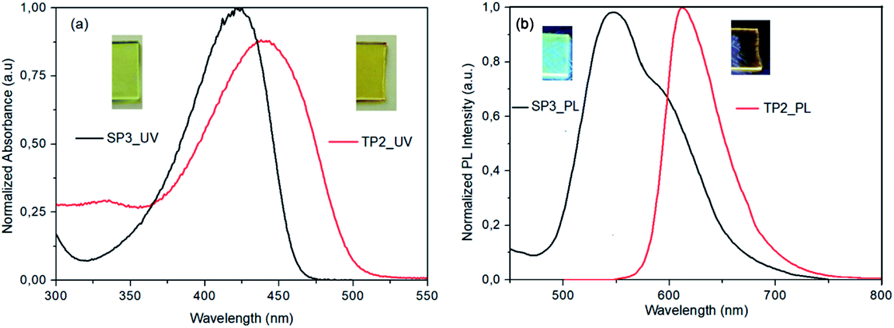 | ||
| Fig. 1 (a) Normalized absorption properties (inlet showed the spin coated SP3 and TP2 thin films under day light), (b) photoluminescence spectra (inlet showed the spin coated SP3 and TP2 thin films under UV light at 366 nm) of the SP3 and TP2 polymer films. | ||
The PL spectrum of the SP3 and TP2 polymer films at solid phase was achieved from the excitation from their UV-Vis absorption maxima (424 and 442 nm, respectively) could be seen in Fig. 1. In the PL spectra of SP3 and TP2 polymer films, the peak wavelengths clearly observed in green and orange color region at 546 and 613 nm, respectively. TP2 had narrow PL characteristic than SP3, while the strong and broad band between 500–700 nm centered at about 546 nm with the shoulder at about 591 nm was observed at the solid phase PL spectrum of SP3. The reason for the broadband was the interaction between the double bond subunit in the fluorene and the conjugated polymer main chain. Here, the hexyl side chain on the thiophene unit reduced the interactions between the double bond in the fluorene and the conjugated chain due to create a steric hindrance.
In Table 1, solid state absolute PL quantum yields (PLQY) of the powder form of SP3 and TP2 polymers could be seen and the PLQY values were 18% and 1.2%, respectively. Chromaticity coordinates of SP3 (x: 0.407, y: 0.533) and TP2 (x: 0.345, y: 0.312) were in the white-orange and yellowish-green, respectively (see ESI, Fig. S5†). Here, due to extra conjugation in TP2, the red shift occurred in the absorption and photoluminescence bands, which caused the color to change. The reason of the high quantum efficiency in SP3 was the interaction between the double bond on the fluorene and the conjugated polymer main chain as explained above. This interaction was due to the fact that the hexyl group on the added extra thiophene in TP2 had a barrier effect between the conjugated chain and the double bond.
| Polymer | Quantum yield | Chromaticity coordinate, x | Chromaticity coordinate, y |
|---|---|---|---|
| SP3 | 0.18 | 0.407 | 0.533 |
| TP2 | 0.012 | 0.345 | 0.312 |
To determine redox behaviors of the SP3 and TP2 polymers, cyclic voltammetry (CV) and differential pulse voltammetry (DPV) technique was used (Fig. 2). In the anodic scan at CV of SP3 and TP2, reversible oxidation waves with half wave potential at about Eox/redp,1/2 = 1.37 V and Eox/redp,1/2 = 1.16 V were observed attributed the oxidation of the conjugated polymer main chain, respectively. The oxidation of the TP2 was observed in the lower potential than that of SP3 due to added extra thiophene donor moieties on TP2 polymer. Like oxidation, the reversible reduction waves with half wave potential at about Ered/oxp,1/2 = −1.76 and Ered/oxp,1/2 = −1.63 V were realized in both polymers for stable radical anion formation of SP3 and TP2, respectively. Due to higher electron density of benzotriazole unit in the SP3 polymer system, it needed a more negative potential for the formation of radical anion during the electrochemical reduction when compared to TP2. Overall this result, the accurate HOMO and LUMO levels calculated from the oxidation and reduction potential onset values from the DPV results of SP3 and TP2. The band gap (Eg) values of SP3 and TP2 polymers were found as 2.99 and 2.67 eV, respectively.
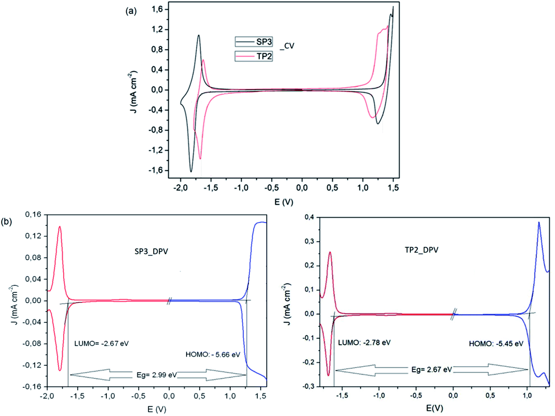 | ||
| Fig. 2 (a) Cyclic voltammetry and (b) differential pulse voltammetry measurements of SP3 and TP2 polymers. | ||
2.2. Theoretical study
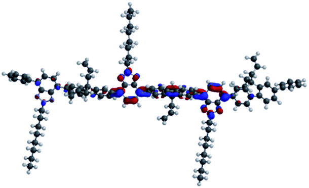
The optimized geometry and the frontier molecular orbitals (FMOs) were investigated using density functional theory (DFT, Spartan 18 software, Wavefunction36) calculations with the B3LYP (Becke 3-parameter-Lee Yang-Parr) with the basis set of 6-311G (d,p).SP3 and TP2 were fully optimized till the third branch at the B3LYP level using the corresponding PM6 equilibrium geometry structures as input. In Table 2 calculated molecular orbitals (HOMO and LUMO) energies (EHOMO and ELUMO) for SP3 and TP2 with B3LYP/6-31G(d,p) level could be seen. FMOs have been investigated experimentally and theoretically by using cyclic voltammetry measurement and DFT calculations, respectively. According to these results, the charge localized on the conjugated donor main chain at HOMO was moved to benzotriazole acceptor moieties. Electrochemical oxidation–reduction results were also supported to the ambipolar behavior of SP3 and TP2.
| Molecule | HOMO (eV) | LUMO (eV) | Eg (eV) |
|---|---|---|---|
| SP3-1 | 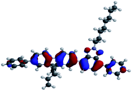 |
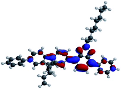 |
3.73 |
| SP3-2 | 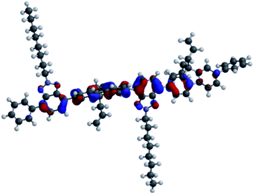 |
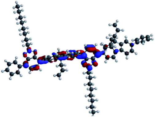 |
3.45 |
| SP3-3 | 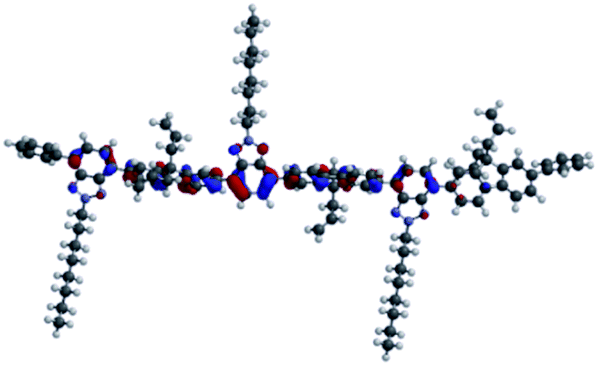 |
 |
3.37 |
| TP2-1 | 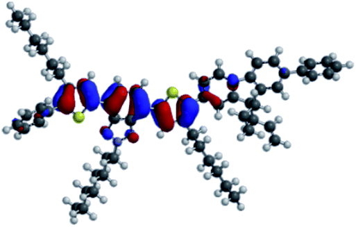 |
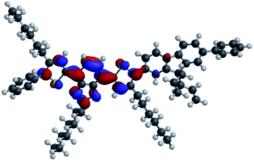 |
2.93 |
| TP2-2 | 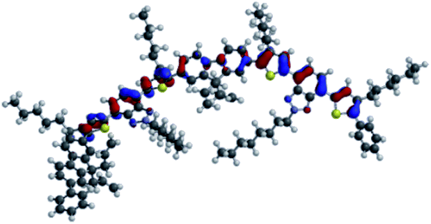 |
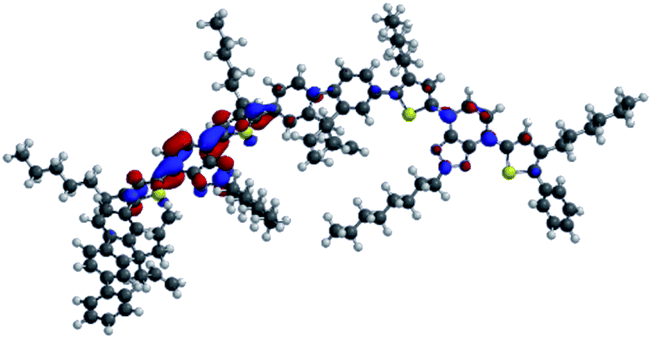 |
2.82 |
| TP2-3 | 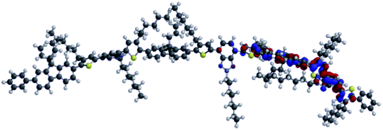 |
 |
2.76 |
2.3. OLED device fabrication and characterization
Fabricated OLED device structure, chemical structures of SP3 and TP2 polymers and their HOMO–LUMO energy levels were presented in Fig. 3. HOMO–LUMO energy values were coherent with each other due to low energy barrier between cathode and emissive layer. Therefore, electron transport from cathode to the SP3/TP2 emissive layer became easier. Also for the anode side, energy barrier (ΔE ∼ 0.3 eV) was low, this provided efficient recombination of the charge carriers in the SP3/TP2 emissive layer.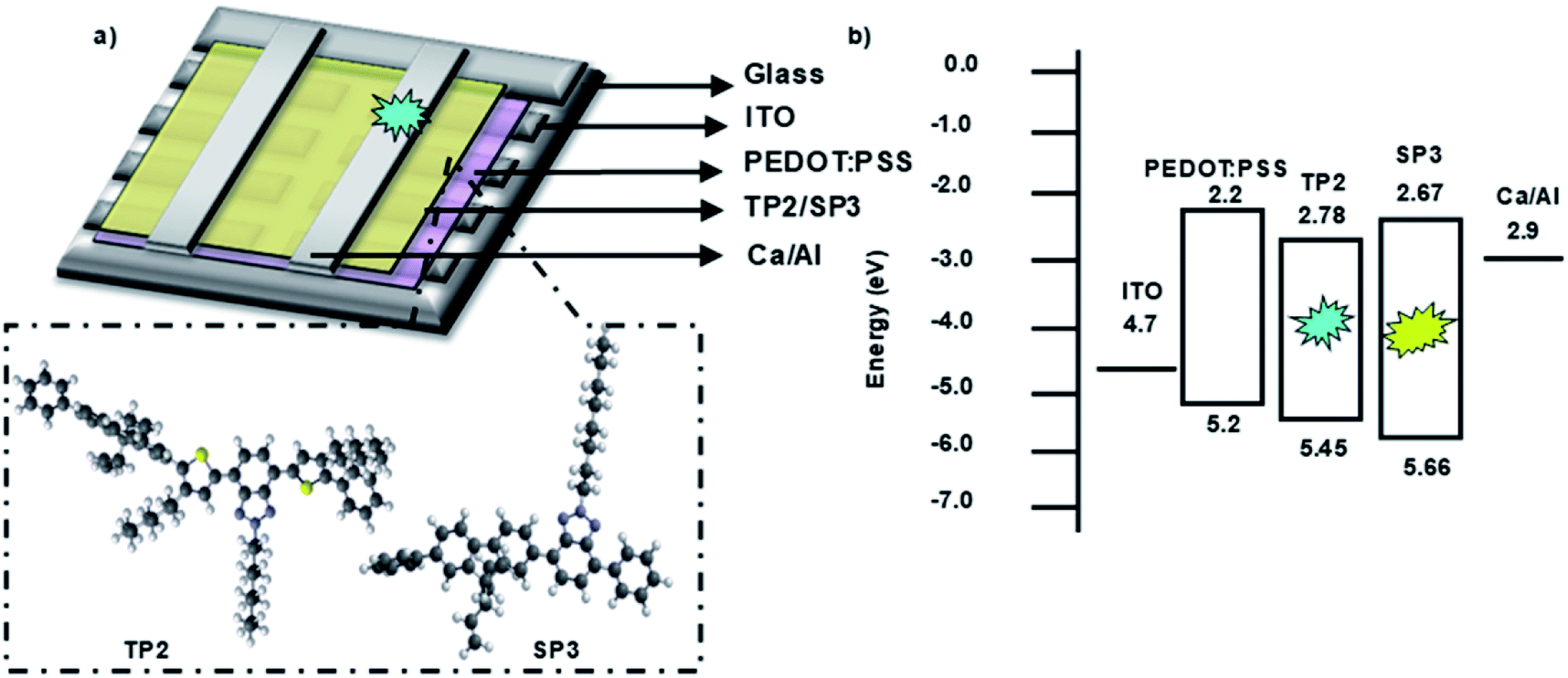 | ||
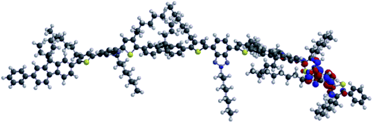
| Fig. 3 (a) 3D Schematic structure of the devices and 3D chemical structures of SP3 and TP2, (b) energy diagram of layers deposited for the OLED devices. | ||
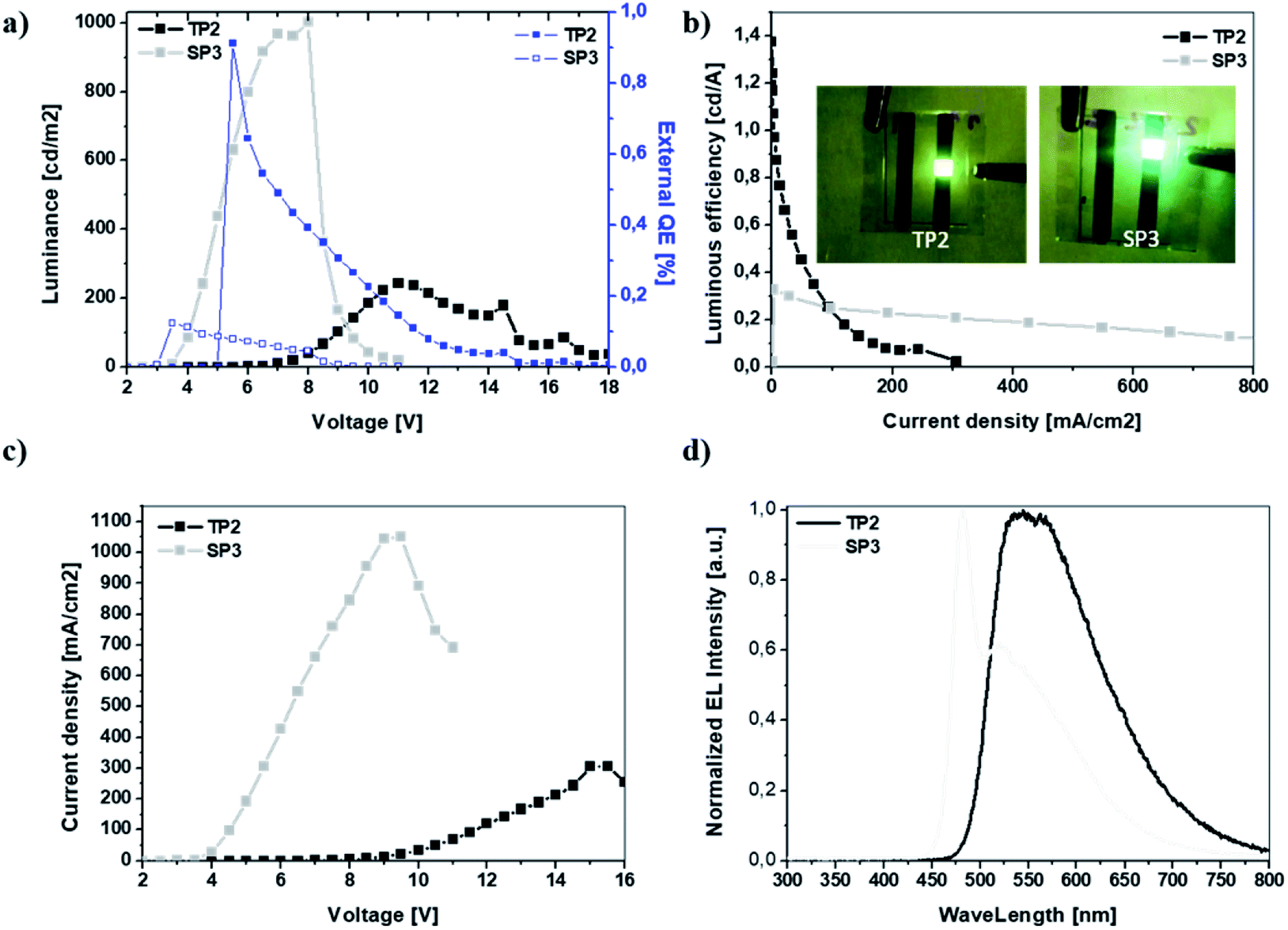 | ||
| Fig. 4 (a) Luminance–voltage, EQE–voltage, (b) luminous (current) efficiency–voltage and inlet presented the light emission of OLEDs with an emissive layer SP3 and TP2 polymers, (c) current density–voltage, (d) normalized EL intensity characteristics. | ||
The EL characteristic of TP2 had the peak wavelength at ∼550 nm which was in the green region of the visible spectrum however FWHM of the EL spectrum was wide and broad almost like white emission that was the intention of this study. SP3 had its peak at 480 nm in blue region, in addition there was a shoulder at 520 nm in green region of visible spectrum. The broadened EL band with the shoulder can be due to the same effect between double bond in fluorene and conjugated polymer main chain like in photoluminescence behavior. Finally, the device characteristics were summarized in Table 3.
| Devices | ||
|---|---|---|
| SP3 | TP2 | |
| Von [V] | 3.0 | 5.8 |
| Lmax [cd m−2] | 1001 | 243 |
| LE [cd A−1] | 0.33 | 1.38 |
| EQE [%] | 0.12 | 0.91 |
| λEL1, λEL2 [nm] | 480, 520 | 550, — |
| CIE [x, y] | 0.32, 0.48 | 0.47, 0.50 |
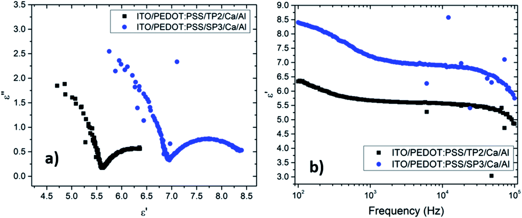 | ||
| Fig. 5 (a) Cole–Cole plots of impedance for fabricated OLED device with TP2 and SP3 films. (b) Variation of real part of dielectric constant depend on frequency for fabricated OLED device with TP2 and SP3. | ||
The depressed semicircles were indicating resistive circuit element which was parallel to internal capacitor.38 Fig. 5 represented impedance phase-shift spectra in all investigated frequency regions for fabricated OLED device with SP3 and TP2. The inset showed electrical equivalent circuit model used for devices. Each transition of phases stood for a different relaxation process.39 It could be seen capacitor-like behavior in high frequency region at about 90 degree and resistive behavior at low frequency region. Both SP3 and TP2 films were demonstrated the similar Cole–Cole plots and same equivalent circuit. Equivalent model could be expressed as in such single-semicircle impedance characteristics in the Cole–Cole plot;
| Z = Req + iXc = R0 + (1/R1 + iωC1)−1. |
When the voltage started increasing, current flowed and emission started from the device, therefore the impedance dependence on frequency could be described by the above formula. The parameters (R0, R1, C1) could be well calculated by using the formula within the help of Cole–Cole plot. The charge carrier life time (τ) could be determined by τ = R1C1 equation.40
In this equation, it was given charge carrier loss arising from recombination with R1. The R0 was small (∼48.7 Ω) and almost unchangeable with applied voltage for the SP3 and TP2 OLED device, thus R0 was considered to originate from the electrode contact. R1 were 635.2 Ω and 753.5 Ω, respectively and also C1 was found 7.3 nF and 5.4 nF, respectively. The parallel resistance R1 in the parallel RC circuit was associated with the layer resistance, while C1 was related with the capacitance of the thin films, namely the RC was relevant to the impedance of the organic layers. Thus, it could be said charge carrier lifetime for SP3 is longer than for TP2.
The Cole–Cole plot of the admittances was one-semicircular characteristics, which was an indicative of no interfacial layer was formed between the organic layers and the cathode contact41 and that the organic layers could be represented as a parallel resistor–capacitor circuit. Although the SP3 and TP2 OLED device consisted of more than two layers, the two-blocked electrical equivalent circuit could be used to ideally fit an experimental impedance response. The thickness of the SP3, TP2 and PEDOT:PSS layers were 50 nm, 50 nm and 60 nm respectively. The value of C is the geometric capacitance which calculated by the given formula;
The real (ε′(ω)) and the imaginary (ε′′(ω)) parts of the dielectric constant were described as ε*(ω) = ε′(ω) − ε′′(ω). The frequency (ω = 2πf), dependent real part of the dielectric constants was given in Fig. 5b.
The dielectric constants for all the materials included in a device were calculated by using capacitance throughput.
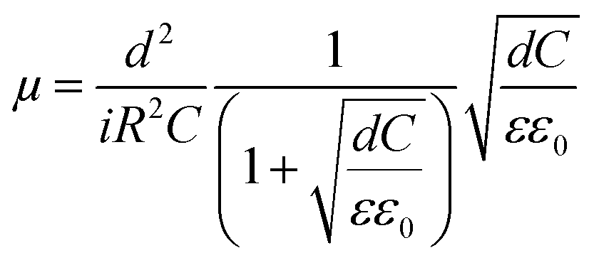
The mobilities could be calculated by using following formula where ε0 is vacuum permittivity (8.85 × 10⁻¹² F m−1), ε relative material permittivity, i current, μ charge carrier mobility.42 Calculated mobility datas were given in Table 4.
| Molecule | ||
|---|---|---|
| SP3 | TP2 | |
| τ | 1.52 × 10⁻⁷ | 1.41 × 10⁻⁸ |
| fc1 | 0.5 × 10⁴ | 0.24 × 10⁴ |
| α1 | 0.764 | 0.924 |
| εs | 8.44 | 6.35 |
| Δε | 2.69 | 1.49 |
| μ | 0.0732 | 0.0166 |
Obtained plots of SP3 and TP2 films were well-matched with the absorption coefficient (α) results. The dielectric strength (Δε = εs − ε∞) of each film were given in Table 4. Investigated films indicated a significant combination of relatively higher and large dielectric strength, yielding a high energy-storage capacity. Analysis of the dielectric relaxation type of these films, relaxation time (τ), and absorption coefficient (α), were determined by the fitting curve of the ε′ − f. The absorption coefficient (α), could take the values from zero to one (0 < α ≤ 1). When the absorption coefficient equals to zero, it represented to standard Debye type relation. If the α parameter was almost zero, this behavior could be defined as nearly Debye type relation.
The non-Debye type occured when the value of absorption coefficient varies between; 0 < α < 1 region.43 The absorption coefficient and the relaxation frequencies also obtained by fitted curves and given in Table 4.
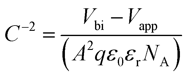
It was seen that the investigation of α parameters indicated non-Debye type relaxation phenomena was occurred. The real part of dielectric constant of TP2 and SP3 films were found around 6.35 and 8.44, in turn. The decreasing of dielectric constant was obviously seen in Fig. 5b with the increment of frequency. It was seen that TP2 and SP3 were quite stable polymer at high relaxation frequency in the interval of 100 to 105 Hz. The critical frequencies (fc) of SP3 and TP2 were evaluated by getting the maximum of the peaks in dielectric loss graphs in Fig. 6. Relaxation frequency shifts to a little higher frequency whereby SP3. Mott Schottky graphs were investigated for OLED devices with SP3 and TP2 as shown in Fig. 7. The capacitance is described by Anderson's equation.44
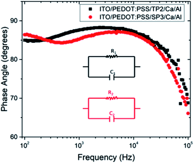 | ||
| Fig. 6 Variation of phase angle depend on frequency for fabricated OLED device with TP2 and SP3. The inset shows electrical equivalent circuit model used for devices. | ||
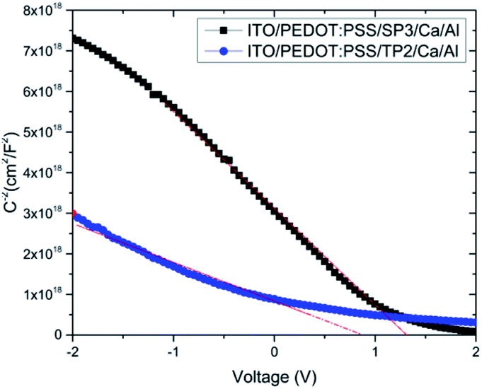 | ||
| Fig. 7 C−2–V plot of devices with SP3 and TP2; experimental data are represented by dots and the fit linear data are represented by a line. | ||
In this equation, εr is the relative dielectric constant, ε0 is the vacuum permittivity, Vbi is built-in voltage, Vapp is applied voltage and NA is the acceptor impurity concentration. Capacitance is proportional to acceptor impurity concentration. The extrapolated intercept in the potential coordinate axis showed that SP3 show larger impact on the built-in potential.
3 Experimental
Synthetic studies of the SP3 and TP2 polymers were given in the ESI (see Fig. S1–S4†). FT-IR spectra were recorded by an Agilent Cary 630 containing ATR attachment (4000–650 cm−1). SP3 and TP2 polymers and PEDOT:PSS (Heraeus Clevios GmbH) were filtered with polytetrafluoroethylene and polyvinylidene fluoride syringe filter, respectively.Before the preparation of OLED device, the ITO patterned substrates (Kintec Company) were cleaned ultrasonically in acetone and isopropanol. Oxygen plasma treatment (Plasma Etch) was applied for 10 minutes to remove organic residues on ITO coated glass-substrates.
Hamamatsu PMA-12 C10027 Photonic Multichannel analyzer and digital multimeter (2427-C 3A Keithley) were used to measure EL, luminance, current efficiency, EQE, current density–voltage characteristics of OLED devices. A profiler (KLA Tencor P-6) was used for thickness determination of organic layers. The optical absorption spectra were measured with FS5 spectrofluorometer (Edinburg Inst, wavelength range of 300–800 nm). Solid state absolute PL quantum yields were obtained with HAMAMATSU Quantaurus-QY. Admittance spectroscopy was worked with GAMRY Reference 3000.
PEDOT:PSS (60 nm) was spin-coated onto the cleaned ITO patterned substrates at 3000 rpm for 30 s and then baked at 150 °C for 15 min on hot plate. The SP3 and TP2 polymers were dissolved in DCB concentration of 8 mg ml−1 and spin coated on top of HIL at 1000 rpm for 40 s then baked on hot plate at 120 °C for 10 min in glovebox. Calcium and cathode contact Al (∼100 nm) were deposited by physical vapor deposition (3 × 10⁻⁶ mbar) technique.
Dielectric measurements of fabricated OLED devices with SP3 and TP2 as described above, were used for the measurement of the capacitive properties by Impedance Analyzer (IA) GAMRY Reference 3000. Electrical characterization of OLED devices with SP3 and TP2 were performed within the frequency range of 10 Hz to 10 MHz.
4 Conclusions
Herein, fluorene-benzotriazole based donor–acceptor polymers namely SP3 and TP2 with double bond subunit were synthesized and characterized by 1H-NMR, GPC, CV, DPV, UV-Vis absorption and photoluminescence in detail. Electrochemical measurements results revealed that SP3 and TP2 polymers had reversible redox behavior both anodic and cathodic regime with band gap of 2.99 eV and 2.67 eV, respectively. The double side reversible redox behavior could be an advantage for the optoelectronic applications such as electrochromic, photovoltaic instead of OLEDs. Besides, the red shift occurred both in UV-Vis absorption and photoluminescence spectra is due to join the extra thiophene electron-donor unit in TP2. OLEDs based on fluorene-benzetriazole based donor–acceptor polymers were fabricated and investigated their performance and EL characteristics due to adding extra thiophene as donor on the main chain. This adjoint thiophene created differences in color coordinates, EL characteristics, light output performances, and impedance analysis. This result guided us towards getting white light with little change due to broader EL characteristic of TP2 than SP3. According to impedance results, it could be said charge carrier lifetime for SP3 was longer than for TP2. The extrapolated intercept in the potential coordinate axis showed that TP2 had lower impact on the built-in potential because TP2 had the 6-carbon alkyl group on the thiophene added extra and a barrier effect between the conjugated chain and double bond. Thus, it was seen that SP3 had larger impact on the built-in potential. These results were found to be compatible with OLED device characterization results.Conflicts of interest
There are no conflicts to declare.Acknowledgements
S. Koyuncu is grateful to Turkish Academy of Sciences GEBIP program and Scientific and Technical Research Council of Turkey (TUBITAK, project #: 114Z064) for financial support.Notes and references
- T. Ito, H. Shirakawa and S. Ikeda, J. Polym. Sci., Polym. Chem. Ed., 1974, 12, 11–20 CrossRef CAS.
- C. K. Chiang, C. Fincher Jr, Y. W. Park, A. J. Heeger, H. Shirakawa, E. J. Louis, S. C. Gau and A. G. MacDiarmid, Phys. Rev. Lett., 1977, 39, 1098 CrossRef CAS.
- J. H. Burroughes, D. D. C. Bradley, A. R. Brown, R. N. Marks, K. Mackay, R. H. Friend, P. L. Burn and A. B. Holmes, Nature, 1990, 348, 352 CrossRef.
- (a) A. J. Heeger, A. G. MacDiarmid and H. Shirakawa, Royal Swedish Academy of Sciences, Stockholm, Sweden, 2000, http://https://www.nobelprize.org/prizes/chemistry/2000/summary; (b) C. K. Chiang, M.A. Druy, S. C. Gau, A. J. Heeger, E. J. Louis, A. G. MacDiarmid, Y. W. Park and H. Shirakawa, J. Am. Chem. Soc., 1978, 100, 1013–1015 CrossRef CAS.
- P. M. Beaujuge and J. R. Reynolds, Chem. Rev., 2010, 110, 268–320 CrossRef CAS PubMed.
- X. H. Zhu, J. B. Peng, Y. Cao and J. Roncali, Chem. Soc. Rev., 2011, 40, 5924–5925 Search PubMed.
- N. S. Sariciftci, L. Smilowitz, A. J. Heeger and F. Wudl, Science, 1992, 258, 1474–1476 CrossRef CAS PubMed.
- M. C. Gather, A. Köhnen and K. Meerholz, Adv. Mater., 2011, 23, 233–248 CrossRef CAS PubMed.
- M. Sun, Q. Niu, R. Yang, B. Du, R. Liu, W. Yang, J. Peng and Y. Cao, Eur. Polym. J., 2007, 43, 1916–1922 CrossRef CAS.
- A. Balan, G. Gunbas, A. Durmus and L. Toppare, Chem. Mater., 2008, 20, 7510–7513 CrossRef CAS.
- A. Balan, D. Baran, G. Gunbas, A. Durmus, F. Ozyurt and L. Toppare, Chem. Commun., 2009, 6768–6770 RSC.
- J. Peet, J. Y. Kim, N. E. Coates, W. L. Ma, D. Moses, A. J. Heeger and G. C. Bazan, Nat. Mater., 2007, 6, 497–500 CrossRef CAS PubMed.
- A. R. Katritzky and B. V. Rogovoy, Chem.–Eur. J., 2003, 9, 4586–4593 CrossRef CAS PubMed.
- A. R. Katritzky and S. Rachwal, Chem. Rev., 2010, 110, 1564–1610 CrossRef CAS PubMed.
- A. R. Katritzky, X. Lan, J. Z. Yang and O. V. Denisko, Chem. Rev., 1998, 98, 409–548 CrossRef CAS PubMed.
- T. Yamamoto, K. Sugiyama, T. Kanbara, H. Hayashi and H. Etori, Macromol. Chem. Phys., 1998, 199, 1807–1813 CrossRef CAS.
- T. Kanbara and T. Yamamoto, Chem. Lett., 1993, 22, 419–422 CrossRef.
- A. Tanimoto and T. Yamamoto, Macromolecules, 2006, 39, 3546–3552 CrossRef CAS.
- A. Tanimoto and T. Yamamoto, Adv. Synth. Catal., 2004, 346, 1818–1823 CrossRef CAS.
- T. Yasuda, T. Imase and T. Yamamoto, Macromolecules, 2005, 38, 7378–7385 CrossRef CAS.
- T. Yamamoto, Bull. Chem. Soc. Jpn., 2010, 83, 431–455 CrossRef CAS.
- Y. Tsubata, T. Suzuki, T. Miyashi and Y. Yamashita, J. Org. Chem., 1992, 57, 6749–6755 CrossRef CAS.
- A. Balan, D. Baran and L. Toppare, Polym. Chem., 2011, 2, 1029–1043 RSC.
- B. Peng, A. Najari, B. Liu, P. Berrouard, D. Gendron, Y. He, K. Zhou, Y. Zou and M. Leclerc, Macromol. Chem. Phys., 2010, 211, 2026–2033 CrossRef CAS.
- Z. Zhang, B. Peng, B. Liu, C. Pan, Y. Li, Y. He, K. Zhou and Y. Zou, Polym. Chem., 2010, 1, 1441–1447 RSC.
- L. Zhang, C. He, J. Chen, P. Yuan, L. Huang, C. Zhang, W. Cai, Z. Liu and Y. Cao, Macromolecules, 2010, 43, 9771–9778 CrossRef CAS.
- E. Kaya, D. H. Apaydın, D. E. Yıldız, L. Toppare and A. Cirpan, Sol. Energy Mater. Sol. Cells, 2012, 99, 321–326 CrossRef CAS.
- E. Kaya, A. Balan, D. Baran, A. Cirpan and L. Toppare, Org. Electron., 2011, 12, 202–209 CrossRef CAS.
- D. E. Yildiz, D. H. Apaydın, L. Toppare and A. Cirpan, J. Appl. Polym. Sci., 2013, 128, 1659–1664 CrossRef CAS.
- S. C. Price, A. C. Stuart, L. Yang, H. Zhou and W. You, J. Am. Chem. Soc., 2011, 133, 4625–4631 CrossRef CAS PubMed.
- J. R. Tumbleston, A. C. Stuart, E. Gann, W. You and H. Ade, Adv. Funct. Mater., 2013, 23, 3463–3470 CrossRef CAS.
- S.-H. Ahn, M.-z. Czae, E.-R. Kim, H. Lee, S.-H. Han, J. Noh and M. Hara, Macromolecules, 2001, 34, 2522–2527 CrossRef CAS.
- Z. Wang, Z. Peng, K. Huang, P. Lu and Y. Wang, J. Mater. Chem. C, 2019, 7, 6706–6713 RSC.
- S. P. Mucur, R. Kacar, C. Meric and S. Koyuncu, Org. Electron., 2017, 50, 55–62 CrossRef.
- A. R. Davis and K. R. Carter, Macromolecules, 2015, 48, 1711–1722 CrossRef CAS.
- P. S. Pro, Wavefunction Inc., 18401 Von Karman Avenue, Suite 370, Irvine, CA 92612, USA Search PubMed.
- F. Kremer and A. Schönhals, Broadband dielectric spectroscopy, Springer Science & Business Media, 2012 Search PubMed.
- T. M. Nahir, Impedance Spectroscopy: Theory, Experiment, and Applications, ACS Publications, 2005 Search PubMed.
- P. Juhasz, J. Nevrela, M. Micjan, M. Novota, J. Uhrik, L. Stuchlikova, J. Jakabovic, L. Harmatha and M. Weis, Beilstein J. Nanotechnol., 2016, 7, 47–52 CrossRef CAS PubMed.
- T. M. Clarke, C. Lungenschmied, J. Peet, N. Drolet and A. J. Mozer, Adv. Energy Mater., 2015, 5, 1401345 CrossRef.
- A. Campbell, D. Bradley, J. Laubender and M. Sokolowski, J. Appl. Phys., 1999, 86, 5004–5011 CrossRef CAS.
- P. Chulkin, O. Vybornyi, M. Lapkowski, P. Skabara and P. Data, J. Mater. Chem. C, 2018, 6, 1008–1014 RSC.
- T. M. Nahir and T. S. Sommers, J. Chem. Educ., 2005, 82, 1089 CrossRef.
- S. Park, E. Cho, D. Song, G. Conibeer and M. A. Green, Sol. Energy Mater. Sol. Cells, 2009, 93, 684–690 CrossRef CAS.
Footnote |
| † Electronic supplementary information (ESI) available. See DOI: 10.1039/d0ra02527e |
| This journal is © The Royal Society of Chemistry 2020 |