
 Open Access Article
 This Open Access Article is licensed under a Creative Commons Attribution-Non Commercial 3.0 Unported Licence
Controlling the electronic and optical properties of HfS2 mono-layers via lanthanide substitutional doping: a DFT+U study
K. O. Obodo a,
G. Gebreyesus*b,
C. N. M. Oumac,
J. T. Obodod,
S. O. Ezeonue,
D. P. Raif and
B. Bouhafsg
a,
G. Gebreyesus*b,
C. N. M. Oumac,
J. T. Obodod,
S. O. Ezeonue,
D. P. Raif and
B. Bouhafsg
aHySA Infrastructure Centre of Competence, Faculty of Engineering, North-West University, South Africa (NWU), 2531, South Africa. E-mail: obodokingsley@gmail.com
bDepartment of Physics, School of Physical and Mathematical Sciences, College of Basic and Applied Sciences, University of Ghana, Ghana. E-mail: garu.gebreyesus@yahoo.com
cHySA Infrastructure Centre of Competence, Faculty of Engineering, North-West University, South Africa (NWU), 2531, South Africa. E-mail: moronaphtaly84@gmail.com
dPhysics Department, University of Nigeria, Nsukka, Nigeria. E-mail: einsteindgreat@gmail.com
eDepartment of Physics/Industrial Physics, Nnamdi Azikiwe University, Awka, Anambra State, Nigeria. E-mail: so.ezeonu@unizik.edu.ng
fPhysical Sciences Research Center (PSRC), Department of Physics, Pachhunga University College, Aizawl-796001, India. E-mail: dibya@pucollege.edu.in
gLaboratoire de Modélisation et Simulation en Sciences des Matériaux, Université Djillali Liabés de Sidi Bel-Abbés, Sidi Bel-Abbés, 22000, Algeria. E-mail: bbouhafs@gmail.com
First published on 23rd April 2020
Abstract
Two dimensional HfS2 is a material with potential applications in the field of photo-catalysis and advanced solid state devices. Density functional theory with the Hubbard U parameter (DFT+U) calculations were carried out to investigate the structural, electronic and optical properties of lanthanide dopant atoms (LN = La, Ce, Pr, Nd, Pm, Sm, Eu, Gd, Tb, Dy, Ho, Er, Tm, Yb and Lu) in the HfS2 mono-layer. The calculated electronic band gap for a pristine HfS2 mono-layer is 1.30 eV with a non-magnetic ground state. The dopant substitutional energies under both Hf-rich and S-rich conditions were evaluated, with the S-rich condition for the dopant atoms being negative. This implies that the incorporation of these LN dopant atoms in the HfS2 is feasible and experimental realization possible. The introduction of LN dopant atoms in the HfS2 mono-layer resulted in a significant change of the material properties. We found that the presence of LN dopant atoms in the HfS2 mono-layer significantly alters its electronic ground states by introducing defect states as well as changes in the overall density of states profile resulting in a metallic ground state for the doped mono-layers. The doped mono-layers are all magnetic with the exception of La and Lu dopant atoms. We found that LN dopant atoms in the HfS2 mono-layer influence the absorption and reflectivity spectra with the introduction of states in the lower frequency range (<1.30 eV). Furthermore, we showed that the applicability of doped HfS2 mono-layers as photo-catalysts is very different compared with the pristine HfS2 mono-layer.
1 Introduction
The study of 2D materials has exploded in recent times after the discovery of graphene.1,2 Other 2D materials have been studied both theoretically and experimentally in search of materials with superior or similar properties to graphene.3–18 These 2D materials offer unique and exotic properties due to their reduced dimensionality associated with quantum confinement compared to their 3D counterparts. Amongst these class of 2D materials is the 2D transition metal dichalogenides (TMDCs) with chemical formula MX2 (where M = Ti, Mo, Nb, W, Hf, Re, etc. and X = S, Se and Te). Their electronic character can be metallic, half-metallic, semi-conducting, insulating, etc.16,18,19 Based on the various electronic characteristics, this group of materials could be applicable for electronic, optical, spintronic, catalytic, and optoelectronic devices, etc.HfS2, a TMDC with promise for low power nano-electronics, high-sensitivity optoelectronic device applications, electron devices as a transistor, with ultra-high photo-responsivity and catalysis properties etc.20–30 The application of HfS2 as a field effect transistor with Ti/Au contacts has been shown to have good electronic characteristics.25 Also, it was demonstrated that HfS2 has strong current saturation, a high on/off ratio, high carrier injection as well as high transport efficiency.22 The presence of lattice imperfections such as O substitution of S or S deficient HfS2, can affect its use as a field effect transistor. This is because an increased band gap with changes in the electron effective mass and formation of strong Hf–O bonds occurs.31,32 Yue et al.33 demonstrated the use of HfS2 multi-layers for molecular detection with the aid of Raman intensities using theoretical and experimental approaches. The presence of excitonic effects in 1T-HfS2 was also evaluated by combining electron energy-loss spectroscopy and computational methods.34 Ibáñez et al.35 showed that the validity of HfS2 calculated properties is strongly influenced by the theoretical method applied. In their study, reasonable agreement was obtained using the generalized gradient approximation (GGA) exchange–correlation functional with the inclusion of van der Waals (vdW) interactions.
The presence of dopant metal atoms has been shown to effectively modify the electronic and magnetic properties of various 2D TMDCs36,37 as well as other 2D materials.15,38 Zhao et al. introduced transition metal dopant atoms into HfS2 mono-layers and showed that these dopant atoms can be stably incorporated with magnetism induced by the V, Cr, Mn, Fe, Co and Cu dopant atoms. Also, Feng et al.39 showed that the magnetic properties of MoS2 mono-layers are modified by Fe–X6 (X = S, C, N, O, F) clusters. Obodo et al.18 and Obodo et al.13 investigated lanthanide and transition metal dopant atoms in the ReS2 and ReSe2 mono-layer, respectively, and showed that the magnetic characteristics are significantly altered resulting in different ground state configuration with potential applications in spintronic devices.
Thus, the current study uses density functional theory (DFT) with the generalized gradient approximation (GGA) for the exchange–correlation functional plus Hubbard U correction (DFT(GGA)+U) to study the pristine and doped HfS2 mono-layers. The present contribution considers the effect of substituting in lanthanide (LN = La, Ce, Pr, Nd, Pm, Sm, Eu, Gd, Tb, Dy, Ho, Er, Tm, Yb and Lu) dopant atoms on the structural, electronic, magnetic, optical and photo-catalytic properties of HfS2 mono-layers. Different substitutional dopant atoms in the HfS2 mono-layer resulted in different electronic and optical characters, which is further described in the manuscript.
2 Computational details
Spin polarized DFT(GGA)+U calculations40–42 for the 1H-HfS2 and LN doped mono-layers were carried out as in the CASTEP43 code. The Generalized gradient approximation based on the PBE approach was applied for the exchange–correlation functional.44 The total energy calculations for the pristine and doped HfS2 mono-layers were carried out using the adequately converged energy cut-off of 600 eV. The Hubbard U correction was introduced to account for the electron–electron correlations due to the presence of LN atoms with unfilled 5f orbitals. The optimized U-parameter of 6 eV presented in the CASTEP code was used.The HfS2 unit cell mono-layer considered consists of one Hf and two S atoms. Next, a 4 × 4 × 1 super-cell of the HfS2 unit cell mono-layer (with 48 atoms, where Hf = 16 atoms and S = 32 atoms) was used to evaluate the presence of LN dopant atoms in HfS2 mono-layers. The LN substitutional doping, which entails replacing one Hf atom with an LN atom (as shown in Fig. 1) was carried out. The Monkhorst–Pack k-point mesh was set to 12 × 12 × 1 (2 × 2× 1) for the pristine HfS2 unit cell (super-cell and doped configurations). The geometric and ionic position of the unit cell was maintained until the forces acting on each atom were less than 10−4 eV Å−1 and 10−7 eV for the total energy convergence. An optimized vacuum distance of about 18 Å was set to prevent out of plane periodic image interactions of the pristine HfS2 unit cell (super-cell and doped configurations). For the super-cell and doped configurations, only the ionic positions were relaxed, using the same convergence criteria as the unit cell. A more refined Monkhorst–Pack grid of 24 × 24 × 1 (4 × 4 × 1) was used to evaluate the electronic and optical properties of the HfS2 unit cell (super-cell and doped configurations) mono-layer.
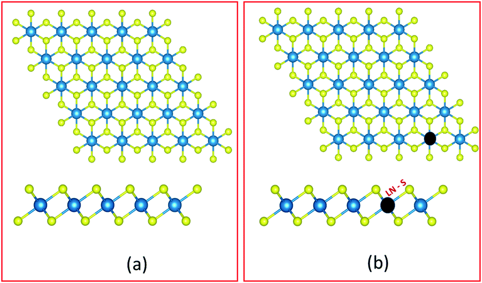 | ||
| Fig. 1 Schematic of the top (top) and side (bottom) view of (a) pristine and (b) doped HfS2 mono-layer crystal structures. The blue, gold and black circles represent the Hf, S and LN atoms, respectively. The measured bond length is indicated as dLN–S. | ||
3 Results and discussion of pristine and lanthanide metal atom-doped HfS2 mono-layers
3.1 Structural properties and stability
HfS2 mono-layer crystallizes in a triclinic structure with the P![[3 with combining macron]](https://www.rsc.org/images/entities/char_0033_0304.gif) m1 space group symmetry as shown in Fig. 1. This has been shown to be dynamically stable with no negative phonon modes.29 The structure has Hf atoms sandwiched between two layers of S atoms. The Hf atom is octahedrally coordinated with the S atoms. The theoretically optimized lattice parameters for the HfS2 unit cell are a = b = 3.6501 Å. These calculated lattice parameters are consistent with previous studies.19,29 The super-cell lattice for the 6 × 6 × 1 HfS2 mono-layer are a = b = 14.6003 Å.
m1 space group symmetry as shown in Fig. 1. This has been shown to be dynamically stable with no negative phonon modes.29 The structure has Hf atoms sandwiched between two layers of S atoms. The Hf atom is octahedrally coordinated with the S atoms. The theoretically optimized lattice parameters for the HfS2 unit cell are a = b = 3.6501 Å. These calculated lattice parameters are consistent with previous studies.19,29 The super-cell lattice for the 6 × 6 × 1 HfS2 mono-layer are a = b = 14.6003 Å.
To determine the likelihood of substituting Hf atoms with the various LN metal atoms in the HfS2 mono-layer lattice, the dopant substitution energy (Esub) was calculated. Esub is the amount of energy required to substitute a host ion with the dopant ion. This was determined using eqn (1), similar to 18, which is analogous to the Zhang–Northrup approach for calculating defect formation energies.45
| Esub = Edoped − Epristine − (μLN − μHf), | (1) |
| Structures | EC | dM–S (Å) | %ΔdM–S | M (μB) | EHf-rich (eV) | ES-rich (eV) | BG (eV) | φ (eV) | %Δφ |
|---|---|---|---|---|---|---|---|---|---|
| Hf | [Xe]6s24f145d2 | 2.551 | 0.00 | 0.00 | −4.69 | 1.30 | 6.12 | 0.00 | |
| La | [Xe]6s25d1 | 2.751 | 7.84 | 0.00 | 1.51 | −3.18 | 0.00 | 5.87 | −4.00 |
| Ce | [Xe]6s24f15d1 | 2.688 | 5.37 | 0.92 | 1.89 | −2.80 | 0.00 | 6.28 | 2.70 |
| Pr | [Xe]6s24f3 | 2.721 | 6.66 | 2.01 | 1.80 | −2.89 | 0.00 | 6.32 | 3.26 |
| Nd | [Xe]6s24f4 | 2.726 | 6.86 | 3.01 | 0.47 | −4.22 | 0.00 | 6.40 | 4.62 |
| Pm | [Xe]6s24f5 | 2.761 | 8.23 | 3.95 | 2.42 | −2.27 | 0.00 | 5.91 | −3.46 |
| Sm | [Xe]6s24f6 | 2.724 | 6.78 | 4.87 | 1.32 | −3.37 | 0.00 | 6.02 | −1.60 |
| Eu | [Xe]6s24f7 | 2.742 | 7.49 | 5.84 | 3.55 | −1.13 | 0.00 | 6.27 | 2.45 |
| Gd | [Xe]6s24f8 | 2.724 | 6.78 | 6.98 | 1.63 | −3.06 | 0.00 | 6.04 | −1.23 |
| Tb | [Xe]6s24f9 | 2.615 | 2.51 | 7.00 | −0.74 | −5.43 | 0.00 | 6.37 | 4.15 |
| Dy | [Xe]6s24f10 | 2.580 | 1.14 | 5.02 | −0.67 | −5.36 | 0.00 | 6.25 | 2.14 |
| Ho | [Xe]6s24f11 | 2.629 | 3.06 | 3.99 | −0.60 | −5.29 | 0.00 | 6.36 | 3.97 |
| Er | [Xe]6s24f12 | 2.676 | 4.90 | 3.02 | 1.32 | −3.37 | 0.00 | 6.35 | 3.84 |
| Tm | [Xe]6s24f13 | 2.663 | 4.39 | 2.01 | 1.76 | −2.93 | 0.00 | 6.34 | 3.53 |
| Yb | [Xe]6s24f14 | 2.670 | 4.66 | 1.02 | 2.53 | −2.16 | 0.00 | 6.36 | 3.87 |
| Lu | [Xe]6s24f145d1 | 2.646 | 3.72 | 0.00 | 0.56 | −4.13 | 0.00 | 5.91 | −3.37 |
The bond length and percentage average change of the bond length for the pristine and LN doped HfS2 super-cells are presented in Table 1. Moving along the LN series, the LN atomic size decreases. This phenomenon is referred to as lanthanide contraction and can influence the properties of materials with LN atoms. The change in bond length for LN doped HfS2 mono-layers does not follow the above stipulated trend in the current investigation. The full understanding of the LN phenomenon was not further investigated. The average percentage change in the bond length of the doped mono-layers in comparison with the pristine HfS2 mono-layer ranges from 1.14% to 8.23% for the Dy and Pm doped mono-layers, respectively. A positive (negative) percentage change implies that substitutional doping would result in an outward (inward) movement of the surrounding S atoms. The Pm doped HfS2 mono-layer showed the maximum outward movement of the surrounding S atom with consequent elongation of the Pm–S bond lengths. Generally, the presence of LN dopant atoms in the HfS2 mono-layer results in minute %ΔdM–S, which has a localized effect in the overall mono-layer. Thus, the introduction of LN dopant atoms in the HfS2 mono-layer results in minimal lattice distortion.
The presence of LN atoms as substitutional dopant atoms was found to change the ground state of the HfS2 mono-layer from non-magnetic to magnetic for some of the LN dopant atoms considered, as presented in Table 1. The inclusion of a single dopant atom in the HfS2 mono-layer can lead to either a non-magnetic or magnetic ground state (ferromagnetic). The total magnetization obtained for the pristine HfS2 mono-layer, and La and Lu doped-HfS2 lattices, are zero (0 μB). These mono-layers are non-magnetic mono-layers. The other considered LN dopant atoms in HfS2 lattices resulted in a magnetic ground state with varying strength as shown in Table 1. We found that the LN dopant atoms with incomplete 4f electrons in their outermost shell give rise to a magnetic ground state, whereas those with completely filled 4f electrons or 5d electrons in the outermost shell were found to be non-magnetic. This is in-line with the general assumption that dopant atoms with 4f electrons in their outermost shell are ferromagnetic with paramagnetism found for those with 5d electrons in their outermost shell. This is consistent with previous investigations.14,18 Thus, these LN dopant atoms could result in the creation of a dilute magnetic nano-layered structure. This magnetic character is further elucidated in Section 3.2 using density of states calculations.
3.2 Electronic properties
The electronic structure of the doped system was investigated and compared to that of the pristine system to gain insight into the nature of impurity states. The calculated density of states profile for the pristine and LN doped HfS2 are presented in Fig. 3. The calculated band gap within the GGA-PBE approximation using ultra-soft pseudo-potential is found to be 1.30 eV, whereas that of the norm-conserving pseudo-potential is 1.36 eV. This is consistent with other studies.21,29 The calculated pristine HfS2 mono-layer shows that the top of the valence band (VB) is dominated by the p states while the bottom of the conduction band (CB) is dominated by the d state. There is marginal contribution from the s-orbitals around the Fermi energy level for the pristine HfS2 crystal structure. The implication from the DOS is that the hybridization of electrons around the Fermi-level is mainly from the p and d states with the s and f states contributing towards deep-lying and high-lying states in the VB and CB, respectively, for the pristine HfS2 mono-layer. The deep-lying and high-lying states were not presented in the current study.After doping with LN atoms, it is evident from Fig. 3 and Table 1 that defect states are introduced within the energy band, or the overall profile of the spin-polarized projected density of states (PDOS) is modified. Consequently, there is a change of the electronic band gap of HfS2 doped mono-layers. These changes within the electronic gap are attributed to the hybridization of the p, d and f-orbitals of the dopant atoms with both the Hf and S atoms. There is marginal contribution from the s-orbitals around the Fermi energy level for these doped HfS2 mono-layers. The Ce, Pr, Nd, Pm, Sm, Eu, Gd, Tb, Dy, Ho, Er, Tm and Yb dopant atoms with 4f electrons in their outermost shell possess 4f-orbitals around the −6 eV to 8 eV range of the DOS profile, whereas the pristine HfS2 mono-layers, La and Lu-doped HfS2 mono-layers does not possess 4f-orbitals around the −6 eV to 8 eV range of the DOS profile. Both the spin-up and down channels close to the Fermi level possess 4f-orbitals in the Ce, Pr, Nd, Pm, Sm doped mono-layers around the −6 eV to 8 eV range of the DOS profile, whereas the Eu, Gd, Tb, Dy, Ho, Er, Tm and Yb doped HfS2 mono-layers possess 4f orbitals in either the spin down or up channels around the −6 eV to 8 eV range of the DOS profile. Thus, the electronic character for these doped HfS2 mono-layers are determined by the hybridization of the p, d and f orbitals. The presence of La, Ce, Pr, Gd, Tb, Dy, Ho and Lu dopant atoms in the HfS2 mono-layer shifted to the top of the VB into the Fermi energy level resulting in a metallic ground state, whereas the presence of Nd, Pm, Sm, Eu, Er, Tm, Yb dopant atoms in the HfS2 mono-layer modifies the energy gap region by introducing new states within the gap in comparison with the pristine HfS2 mono-layer.
There is an observed symmetry and asymmetry in the spin-down and up channels for the non-magnetic (pristine, La and Lu doped HfS2 mono-layers) and magnetic (other considered LN dopant atoms in the HfS2 mono-layers) structures (see Fig. 3), respectively. The observed trend of the total magnetization as a function of the dopant atoms in the HfS2 mono-layers (see Fig. 2) shows that the magnetic moment increases across the lanthanide series and peaks at the Gd and Tb doped HfS2 mono-layer, and further decreases across the lanthanide series to the non-magnetic ground state. This observation is important when considering the choice of LN dopant atom to induce magnetization and the magnitude in 2D systems.
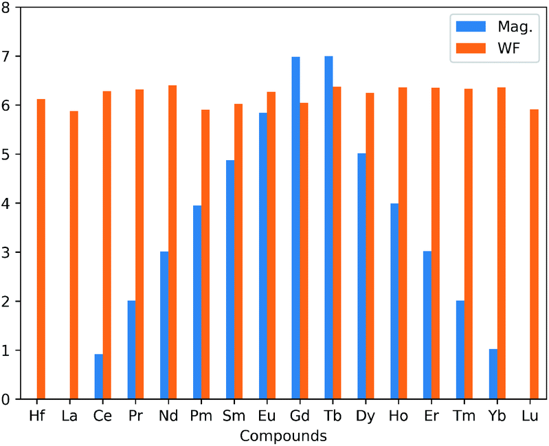 | ||
| Fig. 2 Calculated total magnetic moment (Mag in μB) and the work function (WF in eV) as a function of the lanthanide dopant atoms in HfS2 mono-layers. | ||
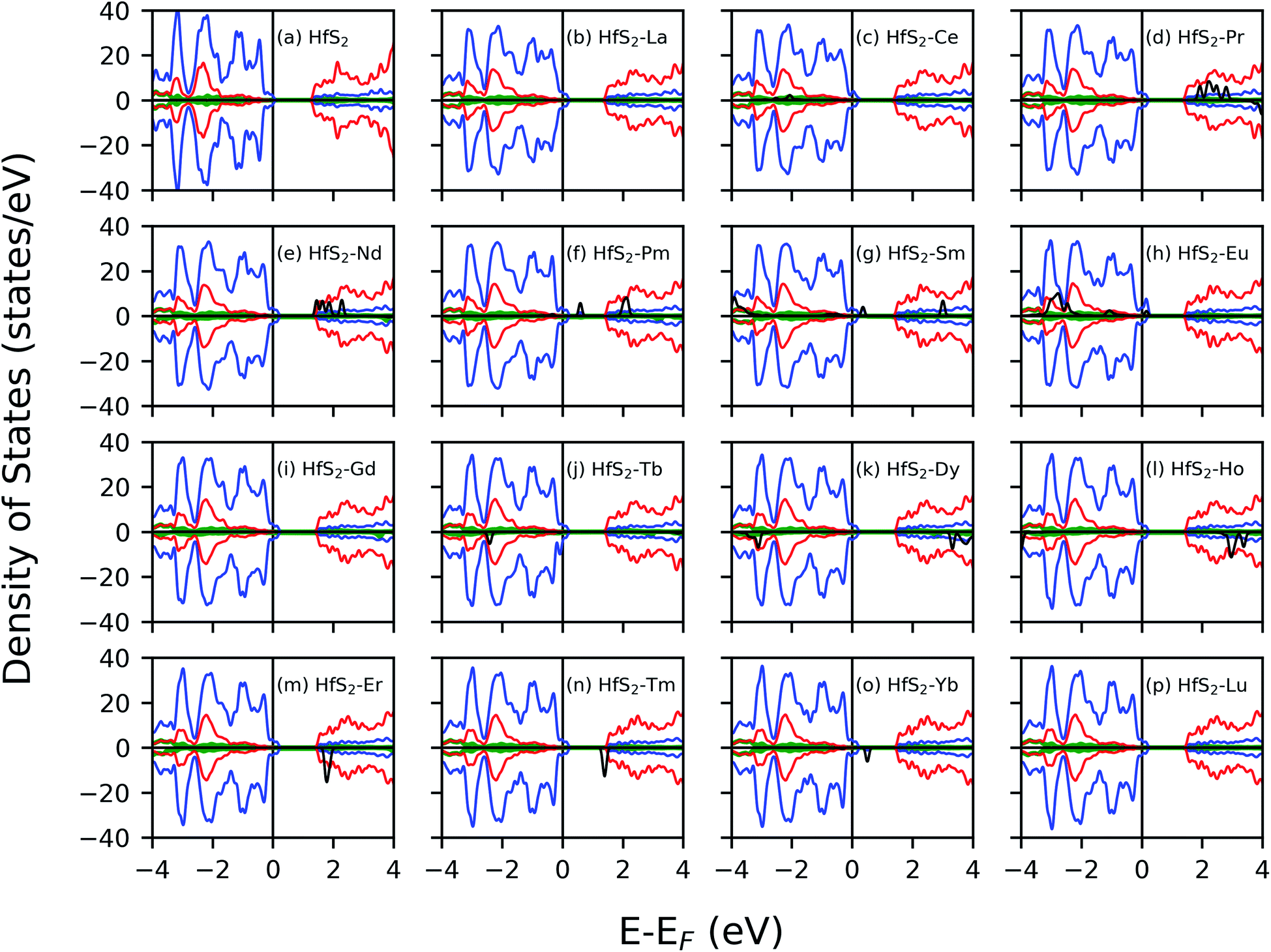 | ||
| Fig. 3 The calculated spin-polarized projected density of states of the pristine and doped HfS2 mono-layer structures. The green, blue, red and black lines represent the s-, p-, d- and f-orbitals, respectively. The energy levels are adjusted with respect to the Fermi energy. | ||
3.3 Work function
The work function (φ) of the considered pristine and doped HfS2 mono-layers are presented in Table 1 and Fig. 2. The φ is an important quantity to determine the suitability of a given material for possible device integration and photo-catalysis. φ can be defined as the minimum amount of work required to remove an electron from the interior of a solid to the vacuum level. φ = Evacuum − EF (or EVBM), where EF is the Fermi energy and EVBM is the energy of the VB maximum. This above equation is equivalent to taking the difference between the Fermi energy from the vacuum level of a given material. The vacuum level is obtained from the average electrostatic potential at the centre of the vacuum region. The variation of the average electrostatic potential in the considered doped mono-layers results in changes to the vacuum level, the VB maximum and CB minimum. Consequently, the changes in the average electrostatic potential results in changes to the calculated φ.The φ and %Δφ show that La, Pm, Sm, Gd and Lu possess lower φ than pristine HfS2 mono-layers unlike the other LN dopant atoms with higher φ. The lower φ implies that it is easier for electrons in those structures to migrate towards the vacuum compared to the ones with higher φ. The implication of the slightly higher φ for the other doped HfS2 mono-layers leads to an increase in the binding affinity of HfS2 mono-layer to electrons, making it less probable for integration into a device. However, in the case of photo-catalysis, the calculated work function is inversely proportional to the catalytic activity of the material. The possibility of the HfS2 mono-layer as a photo-catalyst has been demonstrated in other studies.29 However, further analysis of the photo-catalytic properties of the LN doped HfS2 mono-layers were not considered because the doped structures are metallic and do not fulfil the criteria for use as photo-catalysts.16,46
3.4 Optical properties
We investigated the optical properties of LN metal doped HfS2 mono-layers to elucidate the influence of these dopant atoms. This can be obtained from the real and imaginary part of dielectric function. The matrix elements of the full many-electron wave function for the occupied and unoccupied states can be used to calculate ε2. The Kramers–Kronig relation, which links ε1 to ε2 can be used to determine ε1.47 Several properties can be determined from the dielectric function, such as absorption coefficient, reflectance, refractive index, optical conductivity and energy loss function.The complex dielectric constant, ε(ω), within the linear response regime is given as
| ε(ω) = ε1(ω) + iε2(ω) = N2, | (2) |
Fig. 4 shows the calculated absorption and reflectivity spectra as blue and red lines, respectively. The section shaded in gray represents the pristine absorption spectra for the HfS2 structures. The various dopant atoms in the HfS2 mono-layer lead to a marginal change in the general absorption spectra profile at a higher frequency range (>1.30 eV). The doped structures investigated in this study have reduced the electronic band gap compared to the pristine structures as mentioned in Section 3.2. The implication of LN doping in the HfS2 mono-layer leads to the change in the onset of optical absorption towards the lower frequency level. The onset of the optical absorption frequency for the pristine HfS2 mono-layer is found to be higher than the electronic band gap. For all the doped structures, there is an observed shift in the onset of the absorption spectra with new levels introduced in the IR and UV regions. The intensity of the new level introduced in the absorption spectra due to the LN dopant atoms is low. Thus, the intensity of these lower frequency absorption levels is dependent on the nature of the dopant atoms considered.
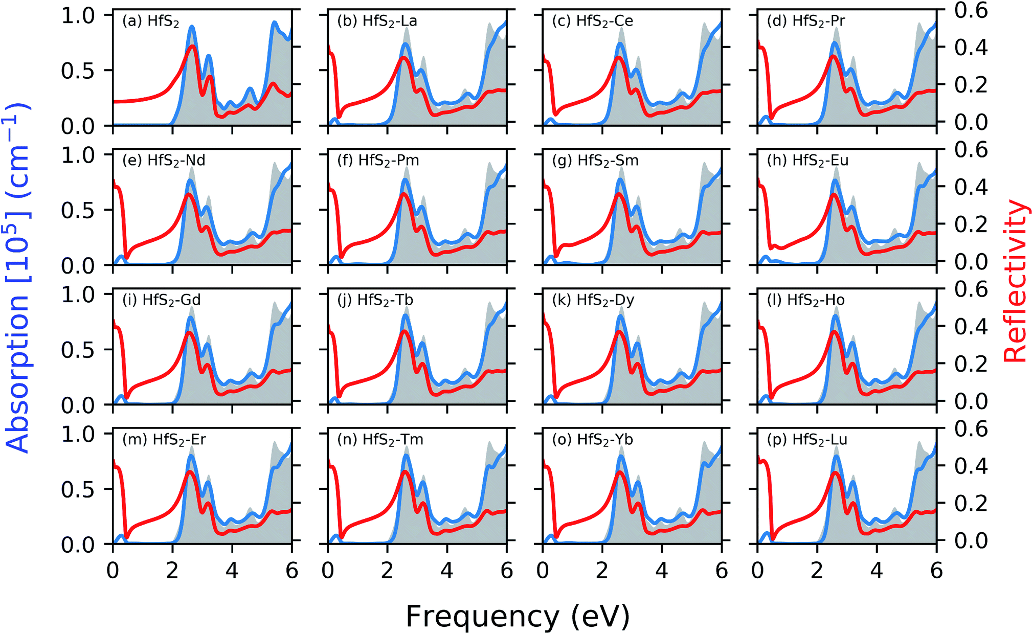 | ||
| Fig. 4 The calculated optical properties as a function of the photon frequency of the pristine and doped mono-layer HfS2 structures. The red and blue lines represent the reflectivity spectra and absorption spectra, respectively. | ||
The optical reflectivity at the low frequency for the pristine HfS2 mono-layer is found to be altered due to the presence of LN dopant atoms. The pristine HfS2 mono-layer shows an intensity peak in the reflectivity spectra at around 2 eV, and other associated lower intensity peaks. There is an observed spike in the reflectivity intensity close to the 0 eV frequency, which is absent from the pristine HfS2 mono-layer. This can be attributed to the metallic character of the electronic structure observed in the presence of LN dopant atoms. The highest reflectivity intensity due to the presence of LN dopant atoms in the HfS2 mono-layer is lower than the pristine mono-layer. Thus, the presence of these LN dopant atoms alter the reflectivity spectra and intensity. It is evident from this study and other investigations18,49 that the nature of dopant atoms results in changes to the optical properties of HfS2 mono-layers. Thus, the obtained results illustrate that LN-doped HfS2 mono-layers would enhance the utilization of the solar spectrum, especially in the near-infrared light region due to the observed shift.
4 Conclusion
DFT was applied to investigate the electronic, magnetic and optical properties of LN metal atoms substituting Hf in HfS2 mono-layers. The Esub of HfS2 in the presence of the dopant ions mainly depends on substitutional ions and doping conditions.Considering the calculated dopant substitutional energies, we observed that doping LN metal ions into the HfS2 crystal structure is feasible, with the S-rich condition being preferable. Generally, we found that LN metal atom doping at the Hf site is an effective way to incorporate dopant atoms into the HfS2 structure.
The electronic band gap of HfS2 is reduced in the presence these substitutional dopant atoms resulting in states above the Fermi level for all the LN dopant atoms. Also with the exception of La and Lu, a magnetic character is observed for the LN doped HfS2 mono-layer. The work function changes depending on the dopant atoms. We found that doping with LN atoms induces magnetization in the HfS2 crystal structure, with the exception of La and Lu atoms.
The onset of optical absorption changes due to the presence of the LN dopant atoms in the HfS2 mono-layer. The dopant ions result in a spike close to the 0.0 eV frequency range for the reflectivity spectra. This can be attributed to the influence of the dopant atoms on the electronic character. The absorption spectra for the pristine HfS2 mono-layer changes due to the presence of LN dopant atoms with associated low frequency peaks attributed to the dopant atoms. This study showed that by doping 2D materials such as HfS2 mono-layers, the electronic, magnetic and optical properties can be modified, with potential applications in the design of tunable electronic, optoelectronic and magneto-optic devices.
Conflicts of interest
There are no conflicts to declare.Acknowledgements
The authors thank the Centre for High Performance Computing (CHPC) in Cape Town, South Africa, for the computational resources used in this study. KOO acknowledges the HySA-Infrastructure Centre of Competence, Faculty of Engineering, North-West University for their financial support.References
- K. S. Novoselov, A. K. Geim, S. V. Morozov, D. Jiang, Y. Zhang, S. V. Dubonos, I. V. Grigorieva and A. A. Firsov, Science, 2004, 306, 666 CrossRef CAS PubMed.
- A. K. Geim and K. S. Novoselov, Nat. Mater., 2007, 6, 183–191 CrossRef CAS PubMed.
- K. Obodo, R. Andrew and N. Chetty, Phys. Rev. B: Condens. Matter Mater. Phys., 2011, 84, 1–7 CrossRef.
- F. Xia, H. Wang, D. Xiao, M. Dubey and A. Ramasubramaniam, Nat. Photonics, 2014, 8, 899–907 CrossRef CAS.
- H. Oughaddou, H. Enriquez, M. R. Tchalala, H. Yildirim, A. J. Mayne, A. Bendounan, G. Dujardin, M. Ait Ali and A. Kara, Prog. Surf. Sci., 2015, 90, 46–83 CrossRef CAS.
- J. T. Obodo, K. O. Obodo and U. Schwingenschlögl, New J. Phys., 2015, 17, 93012 CrossRef.
- B. Amin, N. Singh and U. Schwingenschlögl, Phys. Rev. B: Condens. Matter Mater. Phys., 2015, 92, 075439 CrossRef.
- G. R. Bhimanapati, Z. Lin, V. Meunier, Y. Jung, J. Cha, S. Das, D. Xiao, Y. Son, X. M. S. Strano, X. V. R. Cooper, O. L. Liang, S. G. Louie, E. Ringe, W. Zhou, O. S. S. Kim, R. R. Naik, B. G. Sumpter, O. H. Terrones, F. Xia, Y. Wang, J. Zhu, D. Akinwande, N. Alem, J. A. Schuller, R. E. Schaak, Â. M. Terrones and J. A. Robinson, ACS Nano, 2015, 9, 11509–11539 CrossRef CAS PubMed.
- J. H. Yang, Y. Zhang, W. J. Yin, X. G. Gong, B. I. Yakobson and S. H. Wei, Nano Lett., 2016, 16, 1110–1117 CrossRef CAS PubMed.
- C. Tan, X. Cao, X.-J. Wu, Q. He, J. Yang, X. Zhang, J. Chen, W. Zhao, S. Han, G.-H. Nam, M. Sindoro and H. Zhang, Chem. Rev., 2017, 117, 6225–6331 CrossRef CAS PubMed.
- K. Obodo, N. Chetty and J. Obodo, Comput. Mater. Sci., 2017, 128, 373–378 CrossRef CAS.
- P. Paul, P. Chakraborty, T. Das, D. Nafday and T. Saha-dasgupta, Phys. Rev. B, 2017, 96, 035435 CrossRef.
- K. O. Obodo, C. N. M. Ouma, J. T. Obodo and M. Braun, Phys. Chem. Chem. Phys., 2017, 19, 19050–19057 RSC.
- C. N. M. Ouma, S. Singh, K. O. Obodo, G. O. Amolo and A. H. Romero, Phys. Chem. Chem. Phys., 2017, 19, 25555–25563 RSC.
- C. N. M. Ouma, K. O. Obodo, M. Braun and G. O. Amolo, J. Mater. Chem. C, 2018, 6, 4015–4022 RSC.
- K. O. Obodo, C. N. Moro Ouma, J. T. Obodo, M. Braun and D. Bessarabov, Computational Condensed Matter, 2019, 21, e00419 CrossRef.
- C. N. M. Ouma, K. O. Obodo, M. Braun, G. O. Amolo and D. Bessarabov, Appl. Surf. Sci., 2019, 470, 107–113 CrossRef CAS.
- K. O. Obodo, C. N. M. Ouma, G. Gebreyesus, J. T. Obodo, S. O. Ezeonu and B. Bouhafs, Mater. Res. Express, 2019, 6, 106307 CrossRef CAS.
- X. Zhao, T. Wang, G. Wang, X. Dai, C. Xia and L. Yang, Appl. Surf. Sci., 2016, 383, 151–158 CrossRef CAS.
- X. Zhao, T. Wang, G. Wang, X. Dai, C. Xia and L. Yang, Appl. Surf. Sci., 2016, 383, 151–158 CrossRef CAS.
- X. Ma, X. Zhao, N. Wu, Q. Xin, X. Liu, T. Wang and S. Wei, Solid State Commun., 2017, 268, 15–19 CrossRef CAS.
- T. Kanazawa, T. Amemiya, A. Ishikawa, V. Upadhyaya, K. Tsuruta, T. Tanaka and Y. Miyamoto, Sci. Rep., 2016, 6, 1–9 CrossRef PubMed.
- H. Lu, Y. Guo and J. Robertson, Appl. Phys. Lett., 2018, 112, 062105 CrossRef.
- C. Yan, L. Gan, X. Zhou, J. Guo, W. Huang, J. Huang, B. Jin, J. Xiong, T. Zhai and Y. Li, Adv. Funct. Mater., 2017, 27, 1–9 Search PubMed.
- X. R. Nie, B. Q. Sun, H. Zhu, M. Zhang, D. H. Zhao, L. Chen, Q. Q. Sun and D. W. Zhang, ACS Appl. Mater. Interfaces, 2017, 9, 26996–27003 CrossRef CAS PubMed.
- D. Wang, J. Meng, X. Zhang, G. Guo, Z. Yin, H. Liu, L. Cheng, M. Gao, J. You and R. Wang, Chem. Mater., 2018, 30, 3819–3826 CrossRef CAS.
- X. Zhao, C. Xia, T. Wang, X. Dai and L. Yang, J. Alloys Compd., 2016, 689, 302–306 CrossRef CAS.
- D. Wang, X. Zhang, G. Guo, S. Gao, X. Li, J. Meng, Z. Yin, H. Liu, M. Gao, L. Cheng, J. You and R. Wang, Adv. Mater., 2018, 30, 1803285 CrossRef PubMed.
- D. Singh, S. K. Gupta, Y. Sonvane, A. Kumar and R. Ahuja, Catal. Sci. Technol., 2016, 6, 6605–6614 RSC.
- X. Zhao, X. Liu, T. Wang and S. Wei, J. Alloys Compd., 2018, 731, 303–309 CrossRef CAS.
- K. Iordanidou, M. Houssa, G. Pourtois, V. V. Afanas’ev and A. Stesmans, ECS J. Solid State Sci. Technol., 2016, 5, Q3054–Q3059 CrossRef CAS.
- K. Iordanidou, M. Houssa, G. Pourtois, V. V. Afanas’ev and A. Stesmans, Phys. Status Solidi RRL, 2016, 10, 787–791 CrossRef CAS.
- X. F. Yue, Y. Liang, J. Jiang, R. G. Liu, S. T. Ren, R. X. Gao, B. Zhong, G. W. Wen, Y. Y. Wang and M. Q. Zou, Nanoscale, 2019, 11, 2179–2185 RSC.
- C. Habenicht, L. Sponza, R. Schuster, M. Knupfer and B. Büchner, Phys. Rev. B, 2018, 98, 38–43 CrossRef.
- J. Ibáñez, T. Woźniak, F. Dybala, R. Oliva, S. Hernández and R. Kudrawiec, Sci. Rep., 2018, 8, 1–10 CrossRef PubMed.
- Y. C. Cheng, Z. Y. Zhu, W. B. Mi, Z. B. Guo and U. Schwingenschlögl, Phys. Rev. B: Condens. Matter Mater. Phys., 2013, 87, 2–5 Search PubMed.
- X. J. Zhang, X. C. Wang and W. B. Mi, Solid State Commun., 2015, 212, 35–40 CrossRef CAS.
- L. F. Yang, Y. Song, W. B. Mi and X. C. Wang, Appl. Phys. Lett., 2016, 109, 002103 Search PubMed.
- N. Feng, W. Mi, Y. Cheng, Z. Guo, U. Schwingenschlögl and H. Bai, Sci. Rep., 2014, 4, 3987 CrossRef PubMed.
- P. Hohenberg and W. Kohn, Phys. Rev., 1964, 136, B864–B871 CrossRef.
- W. Kohn and L. J. Sham, Phys. Rev., 1965, 140, A1133–A1138 CrossRef.
- J. P. Perdew, K. Burke and M. Ernzerhof, Phys. Rev. Lett., 1996, 77, 3865 CrossRef CAS PubMed.
- S. J. Clark, M. D. Segall, C. J. Pickard, P. J. Hasnip, M. J. Probert, K. Refson and M. C. Payne, Z. Kristallogr. - Cryst. Mater., 2005, 220, 567–570 CAS.
- J. P. Perdew and Y. Wang, Phys. Rev. B: Condens. Matter Mater. Phys., 1992, 45, 13244–13249 CrossRef PubMed.
- X. Y. Zhang, E. Abrahams and G. Kotliar, Phys. Rev. B: Condens. Matter Mater. Phys., 1991, 66, 1236–1239 Search PubMed.
- V. Chakrapani, J. C. Angus, A. B. Anderson, S. D. Wolter, B. R. Stoner and G. U. Sumanasekera, Science, 2007, 318, 1424–1430 CrossRef CAS PubMed.
- J. S. Toll, Phys. Rev., 1956, 104, 1760–1770 CrossRef.
- L. Sun, W. Zhou, Y. Liu, D. Yu, Y. Liang and P. Wu, Appl. Surf. Sci., 2016, 389, 484–490 CrossRef CAS.
- K. O. Obodo, L. L. Noto, S. J. Mofokeng, C. N. M. Ouma, M. Braun and M. S. Dhlamini, Mater. Res. Express, 2018, 5, 10622 Search PubMed.
| This journal is © The Royal Society of Chemistry 2020 |