
 Open Access Article
 This Open Access Article is licensed under a Creative Commons Attribution-Non Commercial 3.0 Unported Licence
Preparation and photoelectrochemical properties of BiFeO3/BiOI composites
Yuxuan Lei a,
Yaping Zhang*a,
Wenming Dingb,
Lianqing Yu*b,
Xinpeng Zhoua and
Chi-Man Lawrence Wuc
a,
Yaping Zhang*a,
Wenming Dingb,
Lianqing Yu*b,
Xinpeng Zhoua and
Chi-Man Lawrence Wuc
aCollege of Science, China University of Petroleum (East China), Qingdao, 266580, P. R. China. E-mail: zhangyp@upc.edu.cn
bCollege of Materials Science and Engineering, China University of Petroleum (East China), Qingdao, 266580, P. R. China. E-mail: iyy2000@163.com
cDepartment of Materials Science and Engineering, City University of Hong Kong, Hong Kong, SAR, P. R. China
First published on 16th July 2020
Abstract
BiFeO3 thin films were spin coated onto FTO. BiFeO3/BiOI composites have been successfully synthesized by an electrochemical deposition method. The morphology, structure and optical absorption properties of the as-synthesized samples were characterized via XRD, SEM, and UV-Vis DRS. The effect of the BiOI electrodeposition cycles on the photoelectrochemical properties of the BiFeO3/BiOI composites were investigated. The results showed that the photoelectrochemical properties were enhanced under simulated solar light. The composite could achieve an optimum photocurrent density of 16.03 μA cm−2 at 0 V (vs. Ag/AgCl), which is more than twice that of pure BiFeO3 thin films (6.3 μA cm−2). In addition, the Mott–Schottky curves indicate an improvement in the carrier density of the composite. The enhanced photoelectrochemical properties of the composites can be attributed to the formation of a heterojunction at the interface and the band bending of the ferroelectric material BiFeO3.
1. Introduction
Recently, perovskite BiFeO3 (BFO) has received great attention due to its narrow band gap (2.1–2.7 eV), good chemical stability and low cost.1–3 As a typical representative of ferroelectric materials, the internal electric field induced by self-polarization can facilitate the separation of photogenerated electrons and holes, since the special electric field modulates the chemical potential and surface band bending, which play a crucial role in improving the photoelectrochemical (PEC) properties.4–6 However, the PEC activities of BFO are still unsatisfactory because of its poor charge transport properties and electron–hole recombination.7–9 Based on this situation, many strategies have been proposed to obtain better PEC performances of BFO. Wang et al.3 adapted a BFO thin film with a cobalt-phosphate cocatalyst by a photoassisted electrodeposition method, obtaining a photocurrent density nearly 8 times that of the bare BFO electrode. Baqiah et al.4 introduced Fe3O4 into the BFO matrix to improve the photocurrent performance by narrowing the band gap and reducing the recombination of electron holes. Bera et al.5 decorated BFO nanosheets with Au, and the surface-plasmon effect (SPR) of Au nanoparticles benefited the generation of photoelectrons and holes. As a result, the optimum photocurrent density of the decorated composite increased 4-fold to 2.14 μA cm−2 (0.6 V vs. Ag/AgCl).In research on efficient and stable photocatalyst materials, BiOI has become a research hotpot because of its small band gap (1.72–1.92 eV) and unique layered tetragonal structure. The special layered structure containing [Bi2O2]2+ slabs is interleaved by double slabs of halogen atoms, and the weak interlayer van der Waals interaction and strong interlayer bonding lead to excellent PEC properties.10,11 Accordingly, BiOI can be used to construct a heterojunction structure to improve the PEC properties of materials.12–15 For example, Liu et al.13 constructed a BiOI/BiPO4 p–n heterojunction structure via two-step electrodeposition and obtained an enhanced photocurrent density of 2.5 μA cm−2, which is twice that of bare BiOI and nearly 20 times higher than that of pure BiPO4. Ye et al.15 employed BiOI to decorate ZnO/CdS nanorod arrays to overcome the problem of photocorrosion, and consequently, a long-term stability over 6000 s and a high photocurrent density of 3.04 mA cm−2 (1.75 times that of the ZnO/CdS photoanode) were achieved. Thus, the p–n junction formed between CdS and BiOI could be responsible for enhancing the PEC properties.
Considering the abovementioned unique characteristics of BFO and BiOI, we are curious about the synergistic effect between the spontaneous polarization property of BFO and the peculiar layered structure of BiOI. Malathi et al.16 attempted to fabricate BFO/BiOI composite particles for the photodegradation of RhB but achieved only a low photocurrent density of 0.06 μA cm−2, exhibiting a negligible improvement of 0.02 μA cm−2 over BiFeO3. In this work, BiOI-decorated BFO thin films were prepared by chemical solution deposition and electrodeposition. The photocurrent density of the decorated samples, 16.03 μA cm−2, was more than 2 times larger than that of pure BiFeO3, 6.3 μA cm−2.
2. Experimental section
2.1 Sample preparation
BiFeO3 thin films were synthesized via a chemical solution deposition method, as reported previously.17 Typically, 0.85 g of Bi(NO3)3, 0.8 g of Fe(NO3)3 and 3.36 g of citric acid were dissolved into 4.0 g of ethylene glycol by heating at 90 (±3) °C and stirring for 3 h to form a sol–gel. The sol–gel was spin coated onto FTO at 2300 rpm for 60 s to obtain amorphous BiFeO3 films and then crystallized by annealing at 500 °C for 30 min in a tube furnace. The obtained BiFeO3 thin films were denoted by BFO. The BiOI films were prepared via the electrodeposition method under a three-electrode system.18 The obtained BFO electrode, Pt wire and Ag/AgCl electrode were used as the working, counter and reference electrodes, respectively. To obtain 0.04 M Bi(NO3)3 as the electrolyte, Bi(NO3)3 was dissolved in 100 mL of a 0.4 M KI solution. The pH was adjusted to 1.7 with HNO3, and the Bi(NO3)3 solution was mixed with 40 mL of absolute ethanol containing 0.23 M p-benzoquinone and vigorously stirred for 30 min. Electrodeposition was performed in the abovementioned mixed solution at −0.1 V for 6–12 min, and the as-prepared samples were denoted by BFO/BI-n (n = 6, 8, 10, 12). The experimental progress is shown in Scheme 1.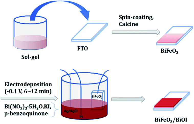 | ||
| Scheme 1 Diagram of the BFO/BI-n sample preparation process. | ||
2.2 Characterization
The crystal structures of the samples were identified by a Dmax-2700 X-ray diffractometer (XRD). The surface morphology was observed using a Hitachi S-4800 field-emission scanning electron microscope (SEM). Transmission electron microscopy (TEM) images were taken with a JEOL JEM-2100 transmission electron microscope. The optical absorption properties were measured with a U-3900 UV-Vis diffuse reflectance spectrometer (DRS), with wavelengths ranging from 280 to 790 nm. The photoluminescence (PL) spectra were obtained using a Hitachi F-7000 fluorescence spectrophotometer. The Fourier transform infrared (FT-IR) spectra were performed via a Bruker Tensor II spectrometer in the wavenumber varying from 4000 to 400 cm−1.The photoelectrochemical (PEC) performance of the samples was investigated by a CHI 760E electrochemical workstation under AM1.5G illumination (I0 = 100 mW cm−2, the wavelength range was 380–780 nm). In a classical three-electrode system, the as-synthesized photoanodes, Pt wire and Ag/AgCl were employed as the working, counter and reference electrodes, respectively. A 1 M Na2SO3 aqueous solution was used as the electrolyte. The photocurrent response plots (I–t plot) were obtained at a 0 V (vs. Ag/AgCl) potential bias under intermittent illumination. The linear scanning voltammetry (LSV) curves were acquired at a scanning rate of 1 mV s−1, and the Mott–Schottky plots were recorded from −0.6 V to 0.6 V (vs. Ag/AgCl) at an applied frequency of 5 kHz.
3. Results and discussion
3.1 Characterization of phase and morphology
The XRD patterns of BiOI, BFO and BFO/BI-n are presented in Fig. 1. For BFO, the pattern indicates that the polycrystalline BFO thin film with a perovskite structure is free from a secondary phase.19 Three main peaks are observed at 2θ = 22.51°, 32.11° and 45.97°, which could be attributed to the (101), (110), and (202) facets of the BiFeO3 perovskite structure (PDF #20-0169), respectively. For BiOI, peaks arise at 2θ = 29.66°, 31.69° and 45.41°, corresponding to the (102), (110) and (200) facets of BiOI (PDF #10-0445), respectively. All the diffraction peaks of the composites can be indexed as BiFeO3 and BiOI, indicating that the composite sample consists of BFO and BiOI, which confirms the successful formation of the heterojunction.20 The intensity of the diffraction peak corresponding to the (110) facet of pure BiOI decreases in the BFO/BI-n (n = 6, 8, 10, and 12) samples, which may be due to the contribution of BiFeO3 to the reorientation of the BiOI crystal growth.21 | ||
| Fig. 1 XRD patterns of pure BFO, BiOI and BFO/BI-n. | ||
Fig. 2 shows the SEM and TEM images of pure BiOI and the BFO/BI-10 composite. The pure electrodeposited BiOI film is composed of a thin two-dimensional plate-like crystal with a length of more than 2 μm, and the special morphology of BiOI, which has a larger specific surface area, favors the combination of BiOI and BFO. No obvious structural changes were observed after BFO and BiOI combined, as illustrated in Fig. 2(b). BFO is cottony when coupled with plate-like BiOI. Moreover, the presence of Bi, O, Fe, and I in the EDS maps (Fig. 2(c–f)) could further confirm the successful fabrication of the BiFeO3/BiOI composite. According to the TEM images of the BFO/BI composite (Fig. 2(g and h)), no core–shell structure was observed.
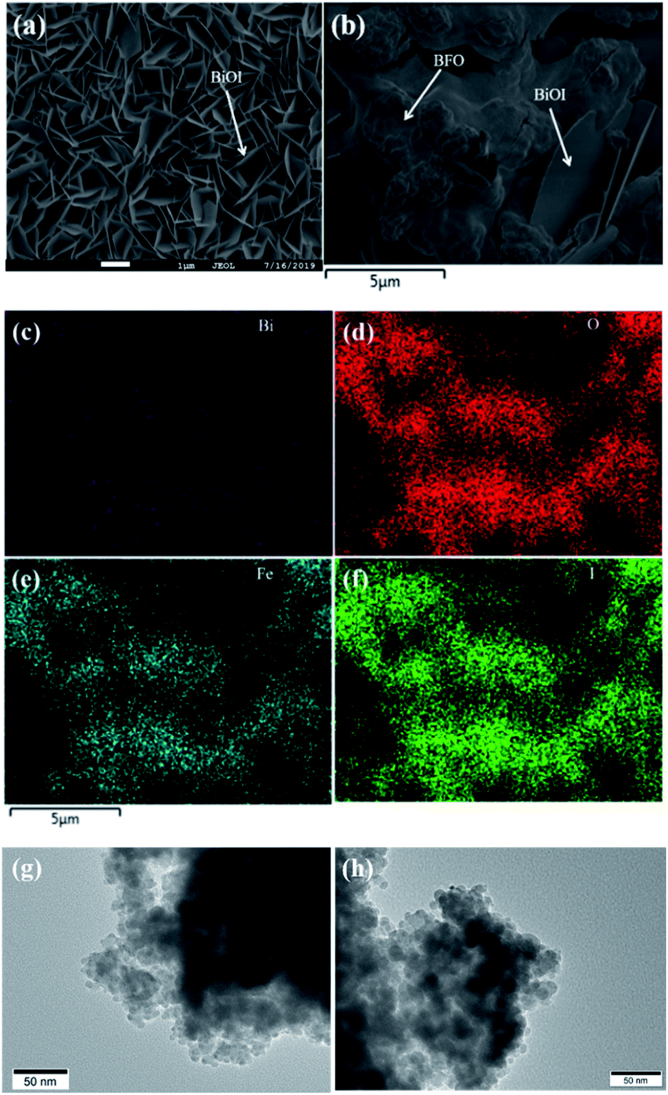 | ||
| Fig. 2 SEM images of (a) pure BiOI and (b) the BiOI/BI composite. (c–f) EDS elemental maps of Bi, O, Fe, and I. (g and h) TEM images of BiOI/BI composite. | ||
3.2 FT-IR analysis
Fig. 3 shows the FT-IR spectra of the pure BFO, BiOI and BFO/BI-10 samples. For pristine BiOI, the band observed at 494 cm−1 can be credited to the symmetrical A2u-type vibration mode of the Bi–O bond.22 In the FT-IR spectrum of pure BFO, the band situated at 553 cm−1 is credited to the Fe–O stretching and bending vibrations.23 The bands at 1620 cm−1 and 3411 cm−1 in the spectrum of pristine BiOI and BFO are attributed to the ν(O–H) stretching and δ(O–H) bending vibrations of the hydroxyl groups. Note that the intensity of the peaks situated at 3411 cm−1 and 1620 cm−1 decreases in BFO/BI-10, which indicates the co-existence of BFO and BiOI.16 Moreover, the characteristic peak of BFO positioned at 553 cm−1 shifts after BFO combines with BiOI, which suggested the formation of a heterojunction between BFO and BiOI.24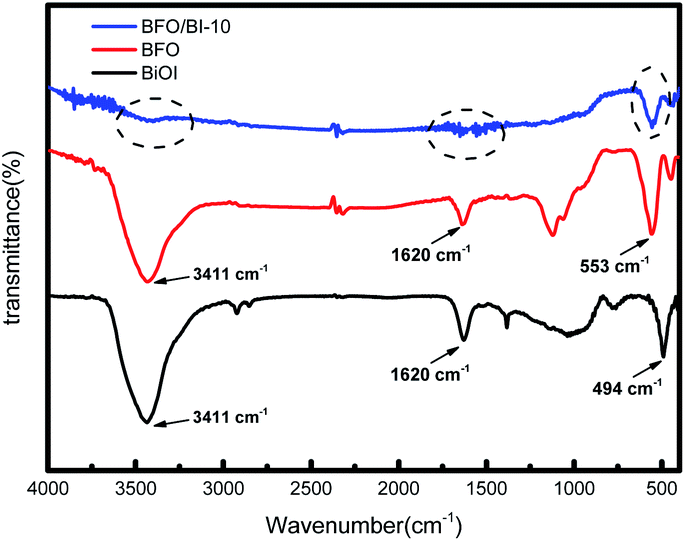 | ||
| Fig. 3 FT-IR spectra of BiOI, BFO and BFO/BI-10. | ||
3.3 Optical absorption properties
The absorption of the synthesized BFO, BiOI and BFO/BI-n thin films was investigated by UV-Vis DRS analysis, as shown in Fig. 4. The composites exhibit better visible region absorption than pristine BFO and BiOI. The band gap energy of the prepared materials was evaluated by the tangent intercept of the plotted linear part,24 and the measured band gaps of pure BFO, BiOI, and BFO/BI-10 were found to be 1.84 eV, 1.93 eV, and 1.81 eV, respectively. The composition of BFO and BiOI extends the range of light absorption and decreases the band gap energy, which assists in the generation of photoelectrons and holes while suppressing the recombination of the photogenerated carriers.25,26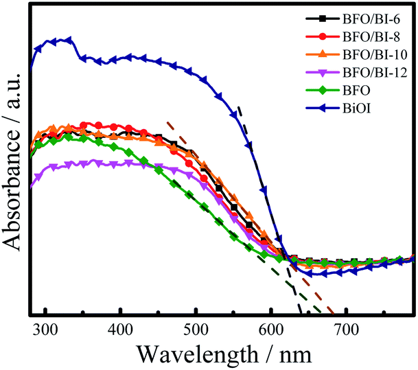 | ||
| Fig. 4 UV-Vis diffuse reflectance spectra of the BFO, BiOI and BFO/BI-n samples. | ||
3.4 Photoelectrochemical properties of BFO/BI-n
Fig. 5(a) shows the I–t plots of the samples obtained at a 0 V bias voltage (vs. Ag/AgCl). Upon simulated one sun illumination, the transient photocurrent of all the composited samples was better than that of the pristine samples. The photocurrent density of BFO/BI-n first increased and then decreased as the number of electrodeposition cycles of BiOI increased, in which BFO/BI-10 reached the highest photocurrent density of 16.03 μA cm−2, which was over twice as high as that of bare BFO (6.3 μA cm−2) and much higher than that of pure BiOI (1.8 μA cm−2). Introducing BiOI composites on the BFO thin films results in the formation of a heterojunction in the interface between BFO and BiOI, which benefits the separation of the photogenerated electrons and holes due to the improvement in the lifetime period of the photoinduced carriers,16,25 thus improving the photocurrent density. However, overdeposition of BiOI will shield BFO layer absorption from light,27,28 resulting in the low photocurrent density of BFO/BI-12.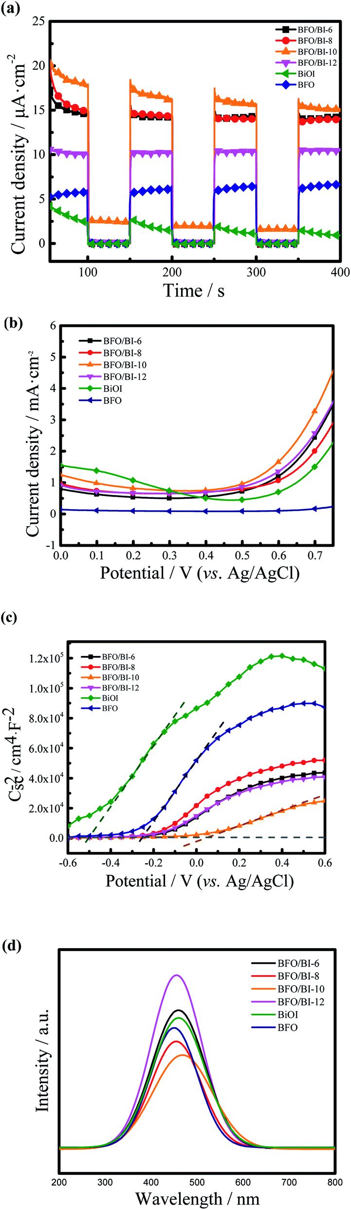 | ||
| Fig. 5 (a) I–t curves, (b) LSV, (c) Mott–Schottky curves, (d) PL spectra of BFO, BiOI and BFO/BI-n. | ||
Fig. 5(b) presents the LSV plots of the as-synthesized samples. The current density of the BFO/BI-n composite was greatly improved across the entire potential range than that of the BFO thin film photoanode. The BFO/BI-10 sample exhibits the best PEC property, with a photocurrent density of 1.658 mA cm−2 at 0.6 V (vs. Ag/AgCl), which is much higher than that of bare BFO (0.102 mA cm−2). The enhancement in the PEC properties could be ascribed to the band bending resulting from the self-polarization of the ferroelectric material BFO, which facilitates the transport of photogenerated electrons and holes.29–31
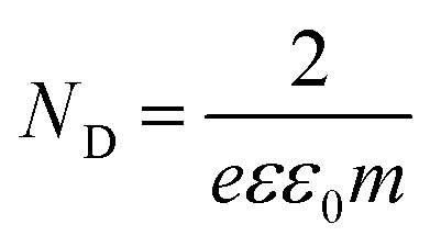
The Mott–Schottky curve can be used to index the density of charge carriers in semiconductors.28,32 In the PEC system, the amplifier photovoltage excited by light charges the space-charge capacitance of the semiconductor, thus influencing the charge carrier density (ND), which can be expressed as
PL spectra can be adapted to investigate the charge recombination progress of materials.35,36 As shown in Fig. 5(d), the PL intensity of BFO/BI-10 was lower than that of the BFO and BiOI photoanodes, indicating that the recombination rate of the photogenerated electrons and holes in the BFO/BI-10 photoanode is lower than that in the BFO and BiOI photoanodes, which contributes to the improvement of PEC performance. The results of the PL spectral analysis confirm the explanation for the improvement in the photocurrent density.
4. Mechanistic analysis
The energy bands of the BFO/BI composite were proposed, as illustrated in Fig. 6. During the process of generating and transporting the photoelectrons and holes in the heterojunction, three main steps are included: first, light is absorbed by the semiconductor, where the coupling of two semiconductors narrows the bandgap, thus increasing light absorption and generating more photoelectron–hole pairs; second, the photoelectrons generated would transfer to the conduction band (CB) from the valence band (VB), and the holes would stay in the VB; and third, since the CB and VB positions of BiOI are higher than those of BFO, the photoelectrons in the CB of BiOI would further transfer to the CB of BFO; furthermore, the holes in the VB of BFO would move to the VB of BiOI, and as a result of this transition, the photogenerated carriers were efficiently separated. Furthermore, the band bending at the interface between BFO and BiOI, which was induced by the spontaneous polarization of BFO, could accelerate carrier transfer,31,37,38 thus improving the separation efficiency of photoelectrons and holes and extending the lifetime of the carriers, which contributes greatly to enhancing the PEC properties of the composite.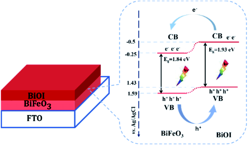 | ||
| Fig. 6 Energy band schematic diagram of BFO/BI. | ||
5. Conclusions
BFO thin films were prepared via the chemical solution deposition method, and two-dimensional plate-like BiOI was fabricated by electrodeposition on pristine BFO thin films. The formation of heterojunctions and band bending at the interface can accelerate the transfer and suppress the recombination of photogenerated electrons and holes. The maximum photocurrent density obtained under solar light was 16.03 μA cm−2 for BFO/BI-10 at 0 V (vs. Ag/AgCl), which is more than twice as high as that of pure BFO (6.3 μA cm−2). The carrier density of all the composite samples is higher than that of pristine BFO and BiOI. The BFO/BI composite, which exhibits excellent photoelectrochemical properties, demonstrates great potential in solar energy conversion applications.Conflicts of interest
There are no conflicts to declare.Acknowledgements
This work is financially supported by National Natural Science Foundation of China (No. 21476262).References
- F. Haydous, N. D. Scarisoreanu, R. Birjega, V. Ion, T. Lippert, N. Dumitrescu, A. Moldovan, A. Andrei, V. S. Teodorescu, C. Ghica, R. Negrea and M. Dinescu, Sci. Rep., 2018, 8, 15826 CrossRef CAS PubMed.
- K. H. Tan, Y. W. Chen, C. N. Van, H. Wang, J. W. Chen, F. S. Lim, K. H. Chew, Q. Zhan, C. L. Wu, S. P. Chai, Y. H. Chu and W. S. Chang, ACS Appl. Mater. Interfaces, 2019, 11, 1655–1664 CrossRef CAS PubMed.
- Y. Wang, D. Chen, S. Wang, J. Liang, L. Qin, X. Sun and Y. Huang, J. Electrochem. Soc., 2019, 166, D308–D314 CrossRef CAS.
- H. Baqiah, Z. A. Talib, A. H. Shaari, M. M. Dihom, M. M. A. Kechik, S. K. Chen, J. Y. C. Liew, Z. Zainal and L. Mohd Fudzi, J. Sol-Gel Sci. Technol., 2019, 91, 624–633 CrossRef CAS.
- S. Bera, S. Ghosh, S. Shyamal, C. Bhattacharya and R. N. Basu, Sol. Energy Mater. Sol. Cells, 2019, 194, 195–206 CrossRef CAS.
- Y. L. Huang, W. S. Chang, C. N. Van, H. J. Liu, K. A. Tsai, J. W. Chen, H. H. Kuo, W. Y. Tzeng, Y. C. Chen, C. L. Wu, C. W. Luo, Y. J. Hsu and Y. H. Chu, Nanoscale, 2016, 8, 15795–15801 RSC.
- Q. Liu, Y. Zhou, L. You, J. Wang, M. Shen and L. Fang, Appl. Phys. Lett., 2016, 108, 022902 CrossRef.
- W. Ramadan and A. Gupta, J. Nanosci. Nanotechnol., 2018, 18, 7804–7810 CrossRef CAS.
- A. K. Vishwakarma, P. Tripathi, A. Srivastava, A. S. K. Sinha and O. N. Srivastava, Int. J. Hydrogen Energy, 2017, 42, 22677–22686 CrossRef CAS.
- L. Hu, Y. Liao, D. Xia, Q. Zhang, H. He, J. Yang, Y. Huang, H. Liu, F. Zhang, C. He and D. Shu, Catal. Today, 2020, 339, 379–390 CrossRef CAS.
- Z. Liu, Q. Wang, X. Tan, Y. Wang, R. Jin and S. Gao, Sep. Purif. Technol., 2019, 215, 565–572 CrossRef CAS.
- M. Li, R. He, S. Wang, C. Feng, H. Wu and H. Mei, Microchim. Acta, 2019, 186, 345 CrossRef PubMed.
- S. Liu, M. Zhao, Z. He, Y. Zhong, H. Ding and D. Chen, Chin. J. Catal., 2019, 40, 446–457 CrossRef CAS.
- Q. Wang, Q. Gao, H. Wu, Y. Fan, D. Lin, Q. He, Y. Zhang and Y. Cong, Sep. Purif. Technol., 2019, 226, 232–240 CrossRef CAS.
- Y.-Q. Ye, G.-H. Gu, X.-T. Wang, T. Ouyang, Y. Chen and Z.-Q. Liu, Int. J. Hydrogen Energy, 2019, 44, 21865–21872 CrossRef CAS.
- A. Malathi, P. Arunachalam, V. S. Kirankumar, J. Madhavan and A. M. Al-Mayouf, Opt. Mater., 2018, 84, 227–235 CrossRef CAS.
- Y. Liu, J. Wei, Y. Liu, X. Bai, P. Shi, S. Mao, X. Zhang, C. Li and B. Dkhil, J. Mater. Sci.: Mater. Electron., 2015, 27, 3095–3102 CrossRef.
- T. W. Kim and K. S. Choi, Science, 2014, 343, 990–994 CrossRef CAS PubMed.
- S. K. Singh, H. Ishiwara and K. Maruyama, Appl. Phys. Lett., 2006, 88, 262908 CrossRef.
- K.-H. Ye, Z. Chai, J. Gu, X. Yu, C. Zhao, Y. Zhang and W. Mai, Nano Energy, 2015, 18, 222–231 CrossRef CAS.
- A. Helal, F. A. Harraz, A. A. Ismail, T. M. Sami and I. A. Ibrahim, Appl. Catal., B, 2017, 213, 18–27 CrossRef CAS.
- A. Malathi, P. Arunachalam, J. Madhavan, A. M. Al-Mayouf and M. A. Ghanem, Colloids Surf., A, 2018, 537, 435–445 CrossRef CAS.
- T. Liu, Y. Xu, S. Feng and J. Zhao, J. Am. Ceram. Soc., 2011, 94, 3060–3063 CrossRef CAS.
- L. Zhang, J. Ran, S.-Z. Qiao and M. Jaroniec, Chem. Soc. Rev., 2019, 48, 5184–5206 RSC.
- J. Low, J. Yu, M. Jaroniec, S. Wageh and A. A. Al-Ghamdi, Adv. Mater., 2017, 29, 1–20 CrossRef PubMed.
- L. Yu, Y. Zhang, J. He, H. Zhu, X. Zhou, M. Li, Q. Yang and F. Xu, J. Alloys Compd., 2018, 753, 601–606 CrossRef CAS.
- L. Yu, Y. Zhang, Q. Zhi, Q. Wang, F. S. Gittleson, J. Li and A. D. Taylor, Sens. Actuators, B, 2015, 211, 111–115 CrossRef CAS.
- Y. Zhang, H. Zhu, L. Yu, J. He and C. Huang, Mater. Res. Express, 2018, 5, 045014 CrossRef.
- L. Li, P. A. Salvador and G. S. Rohrer, Nanoscale, 2014, 6, 24–42 RSC.
- L. Yu, Y. Zhang, J. He, H. Zhu, X. Zhou, M. Li, Q. Yang and F. Xu, J. Alloys Compd., 2018, 753, 601–606 CrossRef CAS.
- J. Song, T. L. Kim, J. Lee, S. Y. Cho, J. Cha, S. Y. Jeong, H. An, W. S. Kim, Y.-S. Jung, J. Park, G. Y. Jung, D.-Y. Kim, J. Y. Jo, S. D. Bu, H. W. Jang and S. Lee, Nano Res., 2017, 11, 642–655 CrossRef.
- L. Yu, L. Rishan, Y. Zhang, Q. Wang, Q. Zhi and K. Dong, J. Optoelectron. Adv. Mater., 2014, 16, 519–523 Search PubMed.
- S. Jeong, J. Song and S. Lee, Appl. Sci., 2018, 8, 1388 CrossRef.
- Y. Zhang, J. He, Q. Yang, H. Zhu, Q. Wang, Q. Xue and L. Yu, J. Power Sources, 2019, 440, 227120 CrossRef CAS.
- H. Huang, Y. He, X. Du, P. K. Chu and Y. Zhang, ACS Sustainable Chem. Eng., 2015, 3, 3262–3273 CrossRef CAS.
- E. M. Steinmiller and K. S. Choi, Proc. Natl. Acad. Sci. U. S. A., 2009, 106, 20633–20636 CrossRef CAS PubMed.
- J. Shi, P. Zhao and X. Wang, Adv. Mater., 2013, 25, 916–921 CrossRef CAS PubMed.
- X. Wu, H. Li, X. Wang, L. Jiang, J. Xi, G. Du and Z. Ji, J. Alloys Compd., 2019, 783, 643–651 CrossRef CAS.
| This journal is © The Royal Society of Chemistry 2020 |