
 Open Access Article
 This Open Access Article is licensed under a Creative Commons Attribution-Non Commercial 3.0 Unported Licence
SERS using two-photon polymerized nanostructures for mycotoxin detection
Qing Liu a,
Koen Vanmola,
Sylvia Lyckebc,
Jürgen Van Erpsa,
Peter Vandenabeelebc,
Hugo Thienponta and
Heidi Ottevaere*a
a,
Koen Vanmola,
Sylvia Lyckebc,
Jürgen Van Erpsa,
Peter Vandenabeelebc,
Hugo Thienponta and
Heidi Ottevaere*a
aDepartment of Applied Physics and Photonics, Brussels Photonics, Vrije Universiteit Brussel and Flanders Make, Pleinlaan 2, B-1050 Brussels, Belgium. E-mail: heidi.ottevaere@vub.be
bDepartment of Chemistry, Ghent University, Krijgslaan 281 – S3, B-9000 Ghent, Belgium
cDepartment of Archaeology, Ghent University, Sint-Pietersnieuwstraat 35, B-9000, Ghent, Belgium
First published on 8th April 2020
Abstract
Improved chemical- and bio-sensing with Surface Enhanced Raman Spectroscopy (SERS) requires nanostuctures that can be flexibly designed and fabricated with different physical and optical properties. Here, we present nano-pillar arrays ranging from 200 nm to 600 nm as SERS substrates for mycotoxin detection that are fabricated by means of two-photon polymerization. We built a nominal shape and a voxel-based model for simulating the enhancement of the electric field of the nano-pillar arrays using the Finite-Difference Time-Domain (FDTD) method. A new model was built based on the Atomic Force Microscopy (AFM) data obtained from the fabricated nanostructures and introduced into a FDTD model. We demonstrated the enhancement behavior by measuring the Raman spectrum of Rhodamine B solutions. Both the simulations and experimental results suggest that the 200 nm nano-pillar array has the highest Enhancement Factor (EF). Besides, we determined the limit of detection of the 200 nm pillar array by performing Raman measurements on Rhodamine B solutions with different concentrations. The detection limit of our 200 nm nano-pillar array is 0.55 μM. Finally we discriminated 1 ppm deoxynivalenol and 1.25 ppm fumonisin b1 in acetonitrile solutions by our SERS substrate in combination with principal component analysis. This versatile approach for SERS substrates fabrication gives new opportunities for material characterization in chemical and biological applications.
Introduction
Surface Enhanced Raman Spectroscopy (SERS) is a surface sensitive detection technique that can enhance the Raman scattering of molecules substantially due to the oscillation of localized surface plasmons by using rough metal surfaces or nanostructures. Nowadays, SERS has been employed in a variety of application domains. The enhancement of Raman scattering makes SERS a powerful tool for chemists to analyse the vibrational and rotational modes of single molecules.1,2 SERS has also been increasingly utilized in biological research and life sciences such as cancer diagnostics,3–5 DNA/RNA identification,6–8 toxin and drug detection.9–11 To achieve these detection goals, SERS substrates with specific surface profiles having a boosted electromagnetic field under laser excitation should be considered. Electrochemically roughened metal electrodes have been used as SERS substrates since 1974, but the low level of enhancement and lack of reproducibility has restricted their applications.12 Noble metal nanospheres ranging from 10–200 nm in colloids or as deposition are typical SERS substrates which can be synthesized by chemical approaches.13–15 Other kinds of irregularly shaped nanoparticles, such as nano-rod, nano-triangles, nano-cubes, nano-stars, nano-cookies and core-shells are increasingly investigated as SERS substrates since they can generate stronger plasmonic oscillation due to the sharp tips or edges, therefore resulting in higher Raman enhancement.16–22 However, the repeatability and reproducibility of SERS measurements with nanoparticles can hardly be guaranteed because of the inhomogeneity of the particles' distributions and shapes. Therefore, nano-pillar arrays, hemisphere arrays, triangle arrays, and other periodical nanostructures have been developed as SERS substrates by means of electrodeposition9 and nanoimprinting lithography23–25 to improve the repeatability and reproducibility. However, these methods are time consuming and less flexible. To fabricate these periodic nanostructures with different dimensions, new polymer or silicon masks must be produced in advance. Chemical etching provides a fast approach for large area SERS substrates manufacturing,26,27 but only nano-pillar arrays can be fabricated with this method.In this paper we present an additive manufacturing method employing two-photon polymerization to fabricate periodic nanostructures as SERS sensing platform. Multiple nano-pillar arrays with different dimensions are printed and characterized. This approach allows fast and flexible prototyping of SERS substrates.28,29 The use of two-photon polymerization lithography can also greatly reduce the complexity and lead time of nanostructure manufacturing for SERS applications by computer-aided design (CAD) and computer-aided manufacturing (CAM). We simulate the boosting of electromagnetic fields for different nano-pillar arrays by the Finite-Difference Time-Domain (FDTD) method.30,31 The simulation output is compared with experimental results of Rhodamine B (RhB) solutions. In a proof-of-concept experiment, we performed SERS measurements on a mix of fumonisin b1 and deoxynivalenol. The spectra of these two types of mycotoxins are analysed with PCA methods and with respect to their vibrational modes.
Material and methods
Fabrication of nanostructures with two-photon polymerization
Two-photon polymerization lithography is a novel 3D additive fabrication technique based on two-photon absorption of photo resins.32 When an ultrashort laser pulse is highly focused into the photoresist, it will initiate two-photon polymerization via two-photon absorption in a small region where the energy is higher than a threshold. This region is the so called ‘voxel’ which represents the minimum feature size we can achieve by two-photon polymerization lithography. Typically, the voxel is defined as an ellipsoid with a specified diameter and aspect ratio which are determined by parameters such as the physical and chemical properties of the photoresist, the intensity and illumination time of the femtosecond laser, the magnification and numerical aperture of the objective lens for focusing. The typical resolution of two-photon polymerization is between 150 nm to 200 nm, but a resolution of 52 nm can be realized under certain circumstances according to the literature.33 By moving the relative spatial position of the voxel with a galvanometric mirror scanner and piezo stages, periodic or perplexing 3D structures can be printed.34In our process, we employ the Nanoscribe Photonic Professional GT 3D printer to fabricate our SERS substrates. Fig. 1 shows the schematic diagram of the GT 3D printer. The GT printer has a 780 nm wavelength femtosecond laser with about 100 fs pulses. The minimum XY feature size we can achieve by Nanoscribe GT with IP-dip photoresin is about 200 nm. The typical printing range of it is 300 × 300 μm2, and the accessible writing area can be up to 100 × 100 mm2. The 3D printing of an individual nano-pillar array with an area of 50 μm × 50 μm takes only 3 to 5 minutes. The fabrication process can be divided into three steps. First, we use CAD software to design the nanostructures with nominal shapes, such as the ideal nano-pillar arrays. These designs can be exported as general stereolithography (STL) files and be imported to the workstation of Nanoscribe GT. Next, according to the system parameters of the 3D printer, such as the magnification of the objective lens, the type of photoresin and the dimensions of the voxel, the workstation compiles the STL files into CNC programs which contain the instructions and parameters the printer will follow. The workstation runs the CNC programs virtually to simulate the two-photon polymerization process. Finally, the Nanoscribe GT runs the CNC programs such that the 3D nanostructures are fabricated. We use a 50× objective lens and IP-dip photoresin (Nanoscribe, Eggenstein-Leopoldshafen/BW, Germany) for the two-photon polymerization manufacturing of the nanostructures.
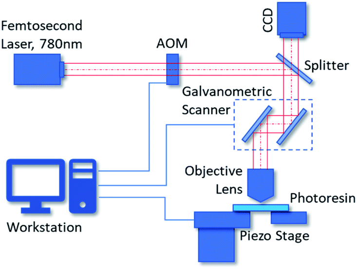 | ||
| Fig. 1 Scheme of the two-photon polymerization system we used for manufacturing nanostructures. (AOM: acousto-optical modulator). | ||
Metrology and simulation
Electromagnetic field enhancement simulation of nanostructures with FDTD method
Although the assignments of SERS have brought many controversies in literature,35 it is generally accepted that the enhancement of SERS stems from two major mechanisms, namely chemical enhancement and electromagnetic enhancement. Chemical enhancement corresponds to the intrinsic properties of the molecule adsorbed on the metallic surface, including the chemical polarity, chemisorption, orientation with respect to the surface, etc36. The chemical mechanism is explained only in specific occasions with low Raman enhancement contribution, and it occurs jointly with the electromagnetic enhancement which is much more dominant.37According to the electromagnetic enhancement hypothesis, the interaction of incident light with the metallic surface of a SERS substrate will generate oscillations of localized plasma dipoles, thereby boosting the electromagnetic field in the region near the surface.38 The boosted region is interpreted as a ‘hotspot’ of the SERS substrate. The electromagnetic enhancement factor, or single-molecule enhancement factor (SMEF) for a molecule located at the hotspot can be expressed in the |ER|2|ES|2 approximation:39
Normally, the Stokes frequency ωS is close to the incident frequency ωR. The expression can further be simplified to:
This implies that the SMEF is proportional to the 4th power of the local field, which provides a simple estimation to mimic the SERS performance via a numerical approach. In this paper we verify the feasibility of two-photon polymerized SERS substrates both theoretically with the FDTD method supported by Lumerical software and experimentally with Rhodamine B detection.
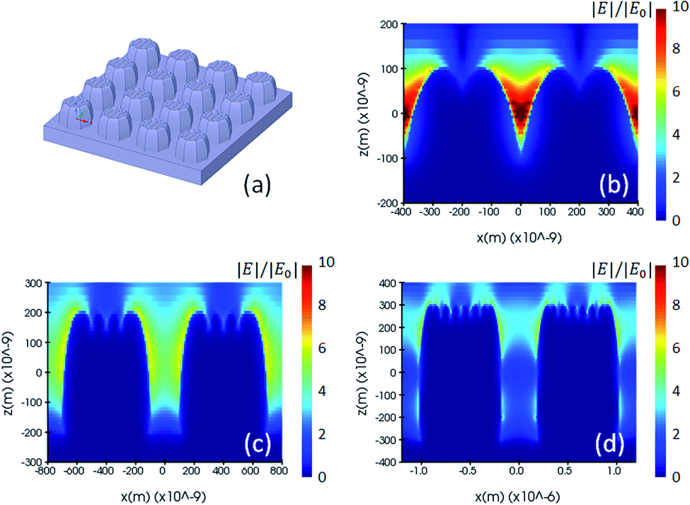
The key parameters of the nano-pillar arrays are the height (H) and diameter (D) of each pillar, and the pitch (P) between them, as shown in Fig. 2(a). In a preliminary study the resolution of two-photon polymerization, pillar arrays with an aspect ratio of 1, i.e. having identical values of height, diameter and pitch, are considered for a range from 200 nm to 600 nm. We build three different simulation models and investigate them for their FDTD electromagnetic solutions, whereby each model corresponds to one step of the nanostructure manufacturing process. The first nominal shape model consists of cylindrical pillars, whereas the second is a voxel-based model, in line with the 3D printing process flow of two-photon polymerization manufacturing, and the third model reflecting the true fabricated shape as measured by Atomic Force Microscopy (AFM).
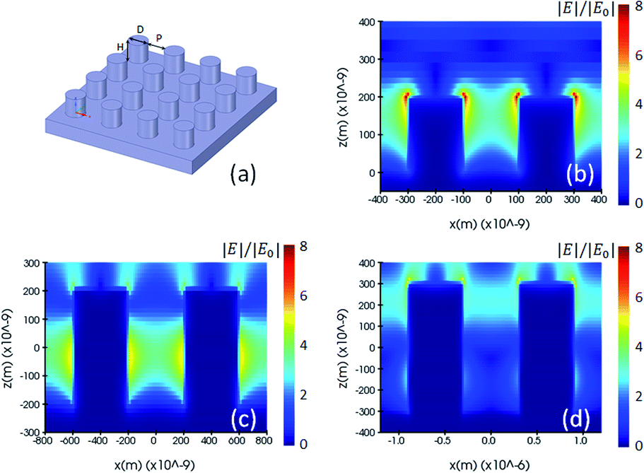 | ||
| Fig. 2 (a) Drawing of a nominal shape model, and (b, c and d) electric field distribution of the 200 nm, 400 nm and 600 nm pillar arrays using the nominal shape model and simulated by the FDTD method. | ||
Fig. 2(a) and 3(a) are illustrations of nano-pillar arrays for the nominal shape model and the voxel-based model, respectively. Fig. 2(b, c and d) show the induced electric field |E|/|E0| with 200 nm, 400 nm and 600 nm nano-pillar arrays in the nominal shape model under 785 nm excitation after FDTD simulations. Fig. 3(b, c and d) show the induced electric field |E|/|E0| with 200 nm, 400 nm and 600 nm nano-pillar arrays in the voxel-based model under 785 nm excitation after FDTD simulations. Here E0 is the amplitude of the excitation electric field, and E is the amplitude of the induced electric field. In the nominal shape model, the leading enhancement of the electric field appears in the edge of the nanostructures. Basically, such perfect shapes are difficult to obtain via two-photon polymerization. In contrast, we notice that the voxel-based model gives rise to complex discrete shapes with cavities and bulges on top of a smoother profile. These complex structures induce extended hotspot sections and higher electric field values in general. But it should be mentioned that the complex structures may also destruct the enhancement in some local areas which we will discuss later. The maximum electric field of the 200 nm pillar array in both the nominal shape model and the voxel-based model is larger than the ones of the 400 nm and 600 nm pillar-arrays, suggesting that 200 nm pillar array has a higher SMEF according to our FDTD simulations.
 | ||
| Fig. 3 (a) Drawing of a voxel-based model, and (b, c and d) electric field distribution of the 200 nm, 400 nm and 600 nm pillar arrays using voxel-based model and simulated by the FDTD method. | ||
After two-photon polymerization fabrication, we employ a 20 nm thick Au layer with a sputtering coater. The fabricated nano-pillar arrays are characterized with Scanning Electron Microscopy (SEM) and Atomic Force Microscopy (AFM). Some of the nano-pillar arrays are shown in Fig. 4. Each of the periodic nanostructure arrays has an effective area of 50 μm × 50 μm and a 1 μm thick base layer to increase the adhesion to the silica glass and its stability. The silica glass has been silanized with 3-(trimethoxysilyl)propyl methacrylate before two-photo polymerization to furtherly improve the adhesiveness. The periodic lines visible in both the SEM and AFM images are due to a stitching process that was used during the 3D fabrication. This effect should not deteriorate the SERS signal in the experiments as the detection area is within the center area of each block, but will be avoided by systematic optimization of the two-photon polymerization process in future work.
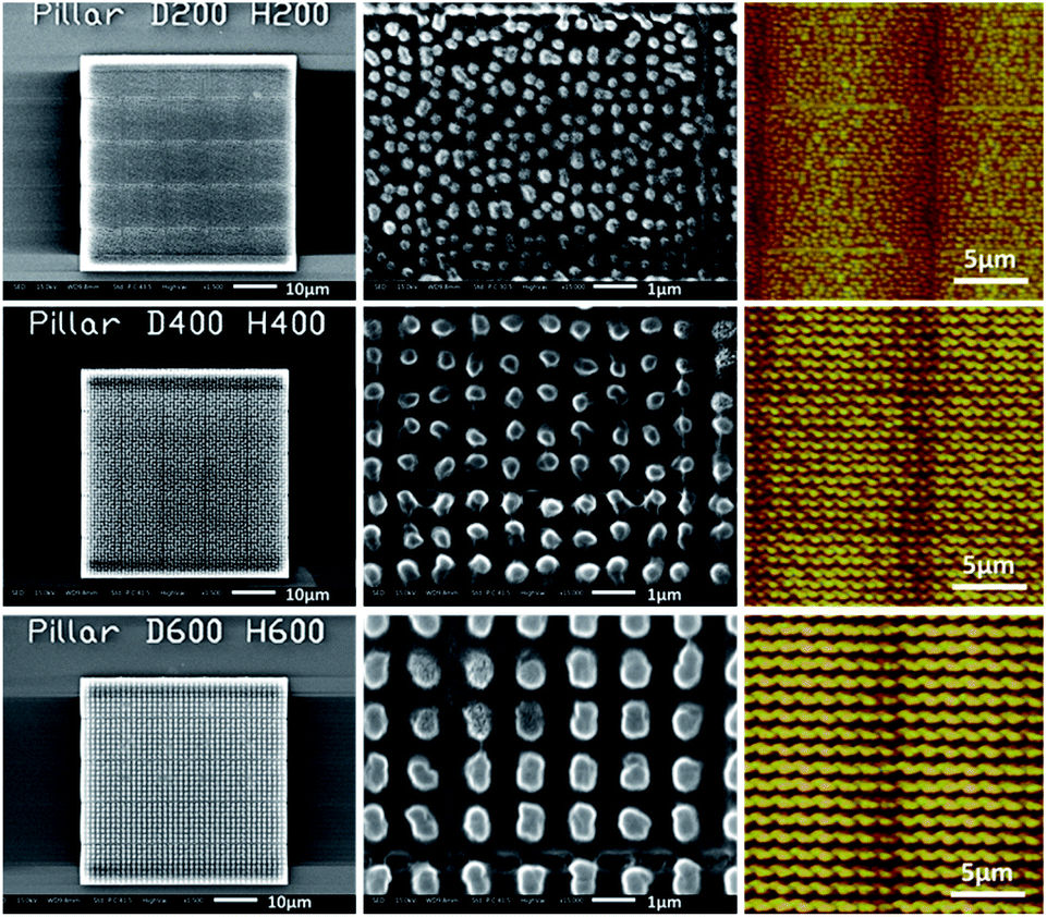 | ||
| Fig. 4 Morphologies of 200 nm, 400 nm and 600 nm nano-pillar arrays. Measured with SEM (column 1 and 2) and AFM (column 3). | ||
We obtained the morphological characteristics of the nano-pillar arrays based on a comprehensive analysis of SEM images and AFM data, shown in Table 1. The measured values of height, diameter and pitch are in good agreement with the designed values. Although the homogeneity of the 200 nm nano-pillar array looks visually less than the ones of the 400 nm and 600 nm nano-pillar arrays, the standard errors of the height, diameter and pitch of the different nanostructures caused by the fabrication errors are similar according to the SEM and AFM measurements. We also notice that, although the heights of the 200 nm and 300 nm structures are still within the confidence interval of the measurements, they are a little bit smaller than the nominal values. This is probably due to the limit of the AFM probe which cannot reach the bottom of the trough when the pitch is very narrow. We build the fabricated shape model based on the 3D data obtained from the AFM.
| Pillar/nm | Height | Diameter | Pitch |
|---|---|---|---|
| a The average and standard deviation for each pillar array are obtained over the measurements within a 20 μm by 20 μm area. | |||
| 200 | 179.7 ± 50.5 | 217.3 ± 38.1 | 228.8 ± 36.1 |
| 300 | 275.3 ± 54.5 | 287.5 ± 21.8 | 304.5 ± 22.4 |
| 400 | 431.1 ± 76.9 | 381.9 ± 35.2 | 358.0 ± 32.0 |
| 500 | 564.4 ± 67.6 | 474.0 ± 43.0 | 473.0 ± 46.6 |
| 600 | 625.0 ± 96.2 | 579.4 ± 35.2 | 573.1 ± 32.3 |
We performed the FDTD simulation on the fabricated shape model and investigated its electromagnetic enhancement. Fig. 5 illustrates the fabricated shape model and the simulated electric field of one cross-section of 200 nm, 400 and 600 nm nano-pillar arrays. Unlike the other two models in which the periodic pattern and induced hotspots are homogeneously distributed, the fabricated model shows a poorer uniformity of the hotspots because the oscillation of localized plasmonic dipoles is much more intricate due to fabrication errors. In this case, the location of molecular adsorption and the detection area are of great importance from a practical point of view. For instance, if a molecule is adsorbed on the region of the middle pillar in the Fig. 5(c), a stronger Raman scattering will be induced compared to the other regions.
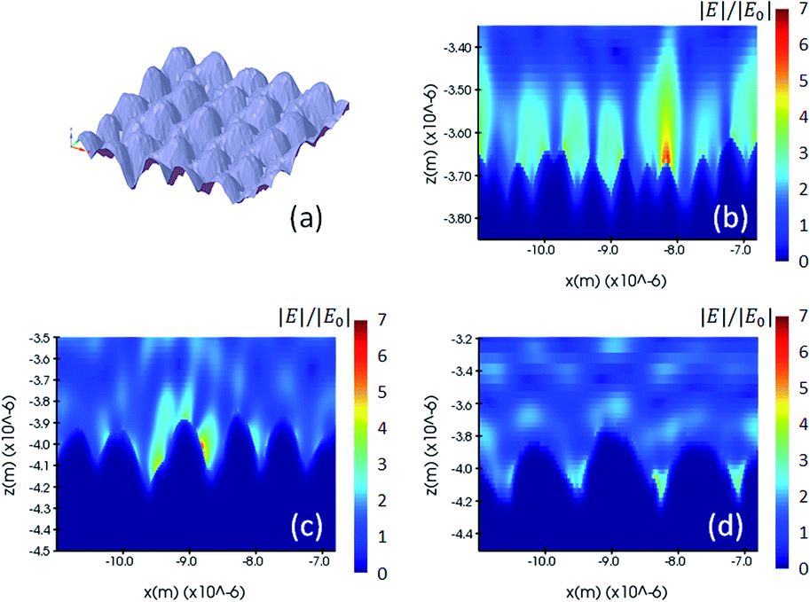 | ||
| Fig. 5 (a) Drawing of a nominal shape model, and (b, c and d) electric field distribution of the 200 nm, 400 nm and 600 nm pillar arrays using the fabricated model and simulated by the FDTD method. | ||
Influence of fabrication errors
During the actual fabrication process, displacement of voxel tracks and distortion of the voxel shape is inevitable due to mechanical vibrations and the accuracy of the printing device, fluctuation of the femtosecond laser power, a change of environmental temperature, etc. To understand the influence of fabrication errors, we performed FDTD simulations considering changes of pitch, height and diameter values of the nano-pillar array, as shown in Fig. 6. For a 400 nm pillar array, a pitch of 50 nm less (b) than the original design (a) will increase the amplitude of the electric field from 7 to 7.5, whereas 100 nm less pitch (c) will increase the amplitude of the electric field to 9.6. As a result, according to the |Eloc(ωR)|4 approximation, the SMEF for 400 nm pillar array with 50 nm and 100 nm displacement in pitch are 1.3 times and 3.5 times more than that of the original, respectively. The errors in the height of the pillar will also change the distribution and intensity of the electric field (d, e and f). If there is a displacement between two adjacent layers in the fabrication process, the diameters of the pillars will be different than our expectation. In some cases, the electric field pattern is similar to that of the pitch errors (g and h), while in other cases the distribution of hotspots is totally relocated from the troughs to the top areas (i). The simulation results indicate that the SMEF of the nano-pillar arrays is more sensitive to horizontal fabrication errors than to vertical errors.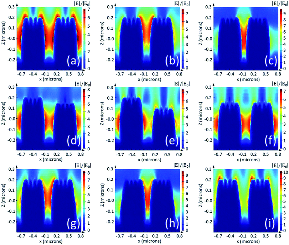 | ||
| Fig. 6 Electric fields of 400 nm pillar array in voxel-based model without (a) and with fabrication errors (b–i). 50 nm and 100 nm closer pitch (b and c) increase the electric field. 50 nm height error (d) and 100 nm height error (e) of one pillar, and all pillars with 50 nm height error (f) have little impact on the electric field. Diameter errors due to displacement of different adjacent layers (g–i) have big impact to the relocation and intensity change of electric fields, as these also reduce the pitch values. | ||
In addition to the errors of the macro profile, the substructures such as nano-cavities, bulges or spikes on top of the nanostructures may result in much more complex enhancement patterns.
Results and discussion
SERS enhancement analysis
To experimentally verify the enhancement factors of the two-photon polymerized SERS substrates, we prepared 10 μM Rhodamine B solutions in ethanol and water respectively and performed Raman measurements utilizing a confocal Raman microscope (Bruker Optics – Senterra). This spectrometer is equipped with a 785 nm laser which is the same wavelength as has been used in our FDTD simulations. The experimental enhancement factor, or the analytical enhancement factor (AEF) can be calculated according to the following equation:39| AEF = (ISERS/NSERS)/(IRef/NRef) |
The chemical structure of Rhodamine B is shown in Fig. 7(a). We placed 30 μL of the Rhodamine B ethanol solution on the SERS substrates, and measured the Raman spectra in the dry state under a 2.5 mW excitation with a 50× objective lens, as show in Fig. 7(b). We can estimate the NSERS with reference to the laser spot size and deposition area under the assumption that the Rhodamine B molecules are evenly delivered on the overall SERS substrate. The reference measurements are conducted by analyzing the Raman scattering of a Rhodamine B aqueous solution since water gives very weak Raman background. We calculated the NRef inside the interaction probe volume of the 50× objective lens under the same excitation. However, we must be aware that the local AEF with inhomogeneous distribution of the molecules may be different than the overall AEF of the SERS substrate, which may be influenced by parameters such as the uniformity of the nano-pillar array, the adsorption of the molecules and the surface tension of the SERS substrate. Fig. 7(c) shows the SERS spectra of Rhodamine B on a 200 nm nano-pillar array. Rhodamine B molecules present distinct enhancement features at 629 cm−1, 1203 cm−1, 1287 cm−1, 1363 cm−1, 1511 cm−1 and 1600 cm−1. The peaks of the Rhodamine B's spectra correspond to the molecular vibrational modes as listed in Table 2.
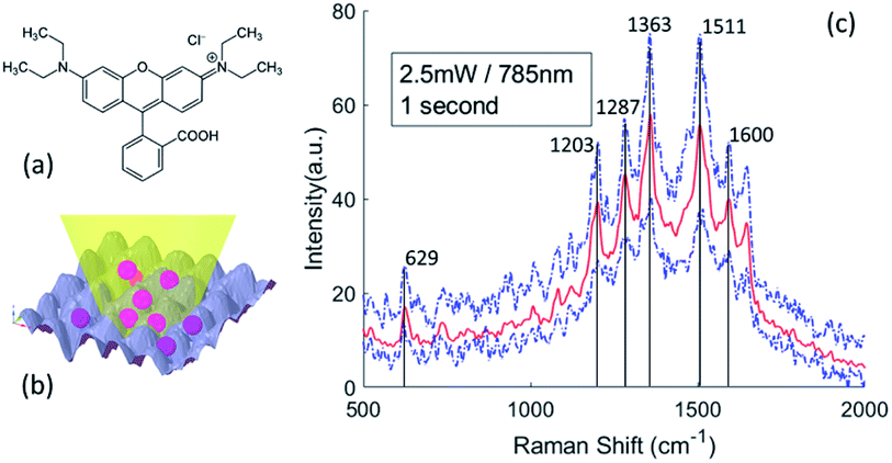 | ||
| Fig. 7 (a) Chemical structure of RhB; (b) scheme of SERS measurement; (c) average Raman spectra of 10 μM RhB obtained with 200 nm pillar arrays under a 785 nm wavelength and 2.5 mW laser excitation with 1 second integration time. The dashed lines refer to the upper and lower range of the spectra. Average spectrum is obtained over 16 measurements. | ||
| Literature40–42 | Raman (cm−1) | SERS (cm−1) | Assignment |
|---|---|---|---|
| a ν: stretching, δ: deformation; W: weak; M: medium; S: strong. | |||
| 619 S | 622.5 S | 629.5 S | ν(aromatic C–C) |
| 965–980 W | 978 W | 969 W | δ(ethylene C–H) |
| 1065–1085 W | 1080 M | 1086 M | δ(aromatic C–H) |
| 1130 W | 1115 W | 1126 W | δ(aromatic C–H) |
| 1199 M | 1198 S | 1203 S | δ(aromatic C–H) |
| 1284 S | 1281 S | 1287 S | δ(C–C) |
| 1360 S | 1359 S | 1363 S | ν(aromatic C–C) |
| 1508 S | 1508 S | 1511 S | ν(aromatic C–C) |
| 1591 W | 1595 W | 1600 S | ν(C![[double bond, length as m-dash]](https://www.rsc.org/images/entities/char_e001.gif) C) C) |
| 1644 S | 1647 S | 1652 W | ν(aromatic C–C) |
The Raman peak of Rhodamine B at 1363 cm−1 shows the highest intensity. Therefore, we calculate the AEF corresponding to the ISERS and IRef at 1363 cm−1. Fig. 8 is the comparison of enhancement factors for the three different models obtained by FDTD simulations and the experimental results. A maximum enhancement factor closes to 104 is achieved by our 200 nm nano-pillar array. It is reasonable that smaller structures give rise to a higher enhancement as they can induce stronger oscillation of localized surface plasmons. The voxel-based model shows the best consistency with experimental results. However, one interesting phenomenon we can observe is that the experimental EFs are larger than the simulated EFs except for the 200 nm and 300 nm voxel-based models. This can be explained by the relocation and intensity changes of hotspots due to the fabrication errors mentioned before. It is hard to predict the precise influence of the fabrication errors over the entire SERS substrate, but we believe that the FDTD simulation of the fabricated shape model can give rise to a better reflection of SERS performance if an AFM with higher resolution and smaller probe size can be used. In addition, because the major boosted electric field of them is generated in the edge area, the EFs of the 300 nm to 600 nm nano-pillar arrays in the nominal shape model show less differences.
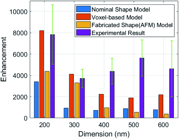 | ||
| Fig. 8 Comparison of enhancement factors for the different models obtained by FDTD simulations and the experiments. The average and standard deviation of each enhancement factor are obtained over 16 measurements on different detection area for a nano-pillar array. | ||
We also performed benchmark measurements of Rhodamine B with two types of commercial SERS substrates from Silmeco (Copenhagen, Denmark) and Horiba, Ltd (Kyoto, Japan) respectively, see Fig. 9. The enhancement factor of our 200 nm pillar array is two orders of magnitude less than that of Silmeco's 106 EF, which can be proven by the spectra. It's noteworthy that our SERS substrate is comparable with Horiba's substrate and performs even better with a higher sensitivity. Therefore, our two-photon polymerized SERS substrate can be used as a powerful tool to study the vibrational modes of molecules.
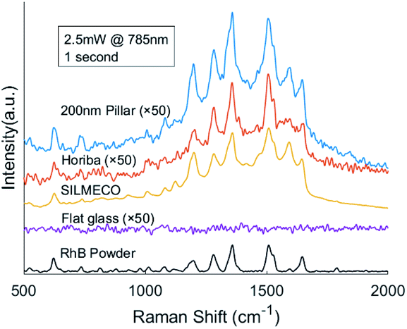 | ||
| Fig. 9 Comparison of 10 μM RhB Raman spectra on different substrates and the Raman spectrum of pure RhB. | ||
Additionally, other types of periodic nanostructures, including nano-hemisphere arrays and nano-grids are printed by two-photon polymerization as well, as shown in Fig. 10. But the Raman performance of these SERS substrates is less than that of the nano-pillar arrays both in simulations and experiments. Therefore, in our later experiments we utilize the 200 nm pillar arrays.
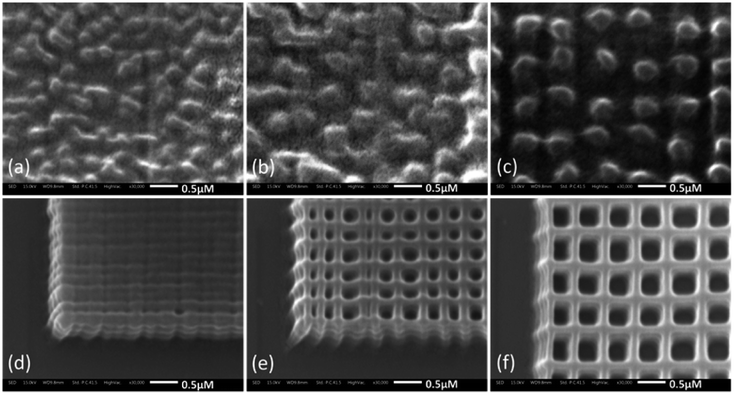 | ||
| Fig. 10 SEM images of 200 nm, 400 nm and 600 nm hemisphere arrays (a–c) and nano-grids with 200 nm, 400 nm and 600 nm spacing (d–f). | ||
SERS substrate calibration
In order to further evaluate the performance of our two-photon polymerized SERS substrates, we measured the Raman spectra of Rhodamine B with different concentrations from 0.5 μM to 1000 μM. The calibration curves of the peak intensity with respect to the concentration are shown in Fig. 11(a). The peak intensity rises as the concentration increases, but the rate of increment gradually falls off. From a certain threshold of concentration, the peak stops increasing and starts to decrease. Because the SERS effective area is just within a few hundred nanometers, the number of hotspots is limited. The molecules can quickly fill the hotspots of the SERS substrate and emit enhanced Raman scattering under the low concentrations. However, as the concentration increases, the number of remaining hot spots begins to decrease with the accumulation of molecules on the metallic surface. And eventually a thick layer is formed that prevents the SERS signal underneath. This can be proved by the microscope images of the original SERS substrate and the SERS substrate with 1 mM Rhodamine B deposition in Fig. 11(b and c).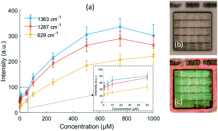 | ||
| Fig. 11 Calibration curves of the 200 nm nano-pillar array showing the peak intensities at 629 cm−1, 1287 cm−1 and 1363 cm−1 with respect to the RhB concentrations (a). Molecules can easily adsorb on the SERS substrate in the low concentration condition (b), but a thick layer of molecules with high concentration will restrain the SERS signal (c). The RhB molecules cover both the nanostructures and the surrounding flat surfaces, for which the interaction of molecules with nanostructures has changed the color of the RhB from red violet to green under white light illumination due to a higher reflectivity at the green light band. | ||
The detection limit of our 200 nm pillar array for Rhodamine B is estimated to be 0.55 μM (5.7 ppm) according to the linear regression of the calibration curve in the low concentration region.43
Application
Mycotoxin detection
SERS is an ideal technique for biochemistry and toxicology because of its low laser intensity, short integration time and small sampling volume required. As proof of concept for our two-photon polymerized SERS substrate, we tested two types of mycotoxins, deoxynivalenol (DON) and fumonisin b1 (FUM). Deoxynivalenol, also known as vomitoxin, is a metabolite of fusarium graminearum which can cause anorexic effects on humans.44 Fumonisin is a metabolite of fusarium verticillioides, one of the most prevalent seed-borne fungi associated with maize.45 Long-term intake of fumonisin contaminated food can greatly increase the risk of esophageal cancer. According to the EU's Mycotoxins Factsheet,46 the limit of deoxynivalenol in unprocessed cereals is 1.25 ppm, and the limit of fumonisin in unprocessed maize is 4 ppm. We measured the Raman spectra of 1 ppm deoxynivalenol and 1.25 ppm fumonisin b1 in acetonitrile with the same equipment under the same excitation as for Rhodamine B. The average spectra of fumonisin b1 and deoxynivalenol obtained with our 200 nm pillar arrays are shown in Fig. 12.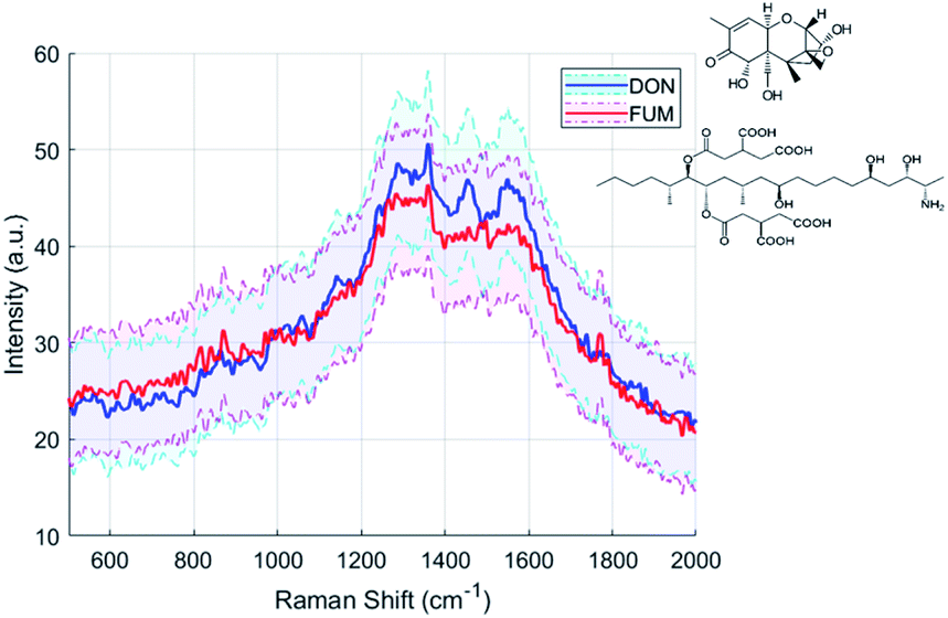 | ||
| Fig. 12 Raman spectra of 1 ppm DON and 1.25 ppm FUM obtained with our 200 nm pillar array SERS substrate under a 785 nm wavelength and 2.5 mW laser excitation with 1 second integration time. The solid line refers to the average spectrum and the shaded area refers to the standard error over 10 measurements. The concentrations of mycotoxins are close to the detection limit of our SERS substrates and therefore it is difficult to recognize the mycotoxins directly. | ||
Principal component analysis (PCA)
The concentrations of mycotoxins are close to the detection limit of our SERS substrates. Therefore, it is difficult to recognize the DON and FUM directly by comparing the spectra, although there are some distinguishing peaks present, such as the 1452 cm−1 and 1140 cm−1 peaks of the DON spectrum, and the 873 cm−1 and 1775 cm−1 peaks of the FUM spectrum respectively. We employed Principal component analysis (PCA) towards a set of Raman spectra observed to discriminate them.47 After PCA transformation, we find that the first three principal components represent 85.9% of the variance, and the two mycotoxins can be clearly distinguished by the second and third principal components, as shown in Fig. 13(a). Raman spectra of DON and FUM show good repeatability with groups of replies, which allow to detect sensible between-sample differences.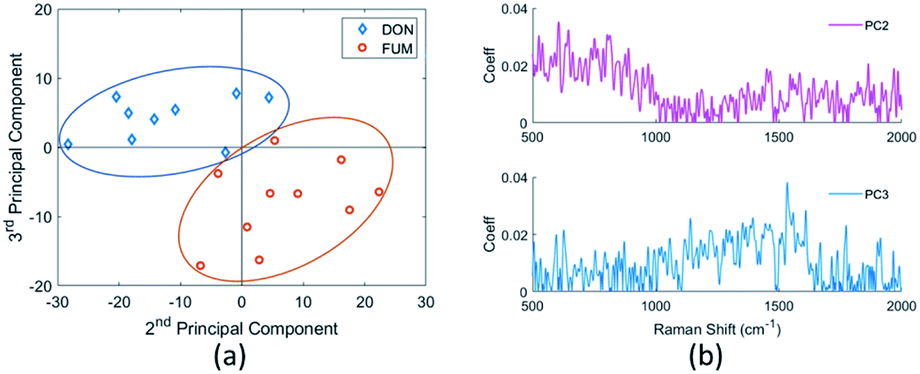 | ||
| Fig. 13 (a) Spectra of DON and FUM are clustered by the scores of the second and third principal components; (b) the coefficients (loadings) of second and third principal components of the mycotoxin spectra observed. | ||
By analyzing the coefficients of the second and third principal components which contains fingerprint Raman shifts information of the two mycotoxins, as shown in Fig. 13(b), combined with literature results, we obtained the characteristic peaks of the two mycotoxins and the corresponding assignments, see Table 3.
| Mycotoxin | Literature48–50 (cm−1) | SERS (cm−1) | Assignment |
|---|---|---|---|
| a ν: stretching, δ: deformation. | |||
| FUM | 760 | 754 | ν(C–C) |
| 868 | 873 | ν(C–O–C) | |
| 1460 | 1466 | δ(–CH3) | |
| 1488 | 1482 | δ(C–H) | |
| 1776 | 1775 | ν(CO) |
|
| DON | 780 | 787 | ν(O–H) + ν(C–H) |
| 855 | 852 | ν(C–H) | |
| 923 | 927 | ν(–CH3) + ν(C–H) | |
| 1139 | 1140 | ν(C–H) | |
| 1293 | 1287 | ν(C–H) | |
| 1430 | 1435 | δ(CC) + ν(–CH3) + ν(C–H) |
|
| 1449 | 1452 | ν(–CH3) | |
Conclusions
We designed and fabricated a series of nano-pillar arrays as SERS substrates ranging from 200 nm to 600 nm by using two-photon polymerization and gold sputtering. To verify the feasibility of these nano-arrays as SERS substrates, we setup a nominal shape model, a voxel-based model, and simulated the induced electric field under 785 nm excitation alongside the nanostructures with the FDTD method. We characterized the morphologies of the different nano-pillar arrays from a comprehensive analysis of SEM images and AFM 3D data. The fabricated shape model based on AFM data is defined as input for the FDTD simulations to determine the induced electric field. The single molecule enhancement factor (SMEF) of different models are calculated based upon the FDTD results.We estimated the experimental enhancement factor (AFE) by analyzing the Raman scattering of 10 μM Rhodamine B solutions in ethanol and water. A maximum enhancement factor closes to 104 is achieved with the 200 nm pillar array. Benchmark measurements have shown that obtained results of our two-photon polymerized SERS substrates are comparable with the ones obtained with the commercial SERS substrates. We compared the experimental enhancement factor with the SMEFs obtained using different models for FDTD simulations, finding that the voxel-based model gives the best consistency with experimental results. In addition, we analyzed the reasons for the differences between simulations and experiments.
Moreover, we evaluated the detection limit of the 200 nm nano-pillar array SERS substrates using different concentrations of Rhodamine B solutions and found the limit to be 0.55 μM. To demonstrate the proof-of-concept of our SERS substrates in an application, we detected the Raman spectra of 1 ppm deoxynivalenol and 1.25 ppm fumonisin b1 solutions. The two types of mycotoxin are discriminated by principal component analysis (PCA). Our two-photon polymerized nano-pillar arrays pave the way for fast prototyping of SERS substrates for biochemical and toxicological research.
The limitation of two-photon polymerization is the restricted structure-sizes of the nano-pillar arrays. But the enhancement factor of the SERS substrates can still be increased by optimizing the nanostructures. Increasing the homogeneity of the nanostructures should be further investigated with respect to parameters such as the optimization of femtosecond laser power fluctuations, the photoresins and the voxel path compiling.
Conflicts of interest
There are no conflicts to declare.Acknowledgements
This research was supported by the China Scholarship Council, FWO (G029919N), the Methusalem and Hercules foundations and the OZR of the Vrije Universiteit Brussel (VUB). The authors would like to thank Dr Michael Stenbæk Schmidt of the Silmeco ApS for providing commercial SERS substrates for benchmark experiments.Notes and references
- A. M. Michaels, M. Nirmal and L. E. Brus, J. Am. Chem. Soc., 1999, 121, 9932–9939 CrossRef CAS.
- E. C. Le Ru, M. Meyer and P. G. Etchegoin, J. Phys. Chem. B, 2006, 110, 1944–1948 CrossRef CAS PubMed.
- S. Lee, H. Chon, J. Lee, J. Ko, B. H. Chung, D. W. Lim and J. Choo, Biosens. Bioelectron., 2014, 51, 238–243 CrossRef CAS PubMed.
- H. Chon, S. Lee, S. W. Son, C. H. Oh and J. Choo, Anal. Chem., 2009, 81, 3029–3034 CrossRef CAS PubMed.
- M. Y. Sha, H. Xu, M. J. Natan and R. Cromer, J. Am. Chem. Soc., 2008, 130, 17214–17215 CrossRef CAS PubMed.
- H. Song, S. Lee, T. Kang and K. Kim, Silver nanoislands based SERS-active substrates for DNAs detection, in Plasmonics in Biology and Medicine XII, International Society for Optics and Photonics, 2015, vol. 9340, p. 93400Y, DOI:10.1117/12.2079003.
- T. Kang, S. M. Yoo, I. Yoon, S. Y. Lee and B. Kim, Nano Lett., 2010, 10, 1189–1193 CrossRef CAS PubMed.
- S. E. J. Bell and N. M. S. Sirimuthu, J. Am. Chem. Soc., 2006, 128, 15580–15581 CrossRef CAS PubMed.
- Y. Zhou, J. Chen, L. Zhang and L. Yang, Eur. J. Inorg. Chem., 2012, 3176–3182 CrossRef CAS.
- P. H. Aoki, L. N. Furini, P. Alessio, A. E. Aliaga and C. J. Constantino, Rev. Anal. Chem., 2013, 32, 55–76 CAS.
- J. F. Li and Z. Q. Tian, Nature, 2010, 464, 392–395 CrossRef CAS PubMed.
- M. Fleischmann, P. J. Hendra and A. J. McQuillan, Chem. Phys. Lett., 1974, 26, 163–166 CrossRef CAS.
- X. Dou, Y. M. Jung, Z. Q. Cao and Y. Ozaki, Appl. Spectrosc., 1999, 53, 1440–1447 CrossRef CAS.
- M. Knauer, N. P. Ivleva, R. Niessner and C. Haisch, Anal. Sci., 2010, 26, 761–766 CrossRef CAS PubMed.
- X. Dou, Y. M. Jung, H. Yamamoto, S. Doi and Y. Ozaki, Appl. Spectrosc., 1999, 53, 133–138 CrossRef CAS.
- T. Huang and X. H. N. Xu, J. Mater. Chem., 2010, 20, 9867 RSC.
- H. Guo, B. Xing, L. C. Hamlet, A. Chica and L. He, Sci. Total Environ., 2016, 554–555, 246–252 CrossRef CAS PubMed.
- A. Reznickova, Z. Novotna, N. S. Kasalkova and V. Svorcik, Nanoscale Res. Lett., 2013, 8, 1–8 CrossRef PubMed.
- Z. Zhang, F. Liao, S. Ma, S. Gao and M. Shao, Surf. Interface Anal., 2015, 47, 398–402 CrossRef CAS.
- L. Rodríguez-Lorenzo, Z. Krpetic, S. Barbosa, R. A. Alvarez-Puebla, L. M. Liz-Marzán, I. A. Prior and M. Brust, Integr. Biol., 2011, 3, 922–926 CrossRef PubMed.
- Q. An, P. Zhang, J. M. Li, W. F. Ma, J. Guo, J. Hu and C. C. Wang, Nanoscale, 2012, 4, 5210 RSC.
- Y. Wang, B. Yan and L. Chen, Chem. Rev., 2013, 113, 1391–1428 CrossRef CAS PubMed.
- H. Wang, K. Lai, Y. Lin, C. Lin and J. He, Langmuir, 2010, 26, 12855–12858 CrossRef CAS PubMed.
- C. Kuo, J. Shiu, Y. Cho and P. Chen, Adv. Mater., 2003, 13, 1065–1068 CrossRef.
- L. Bi, Y. Wang, Y. Yang, Y. Li, S. Mo, Q. Zheng and L. Chen, ACS Appl. Mater. Interfaces, 2018, 10, 15381–15387 CrossRef CAS PubMed.
- M. S. Schmidt, A. Boisen, and H. Jörg, IEEE SENSORS 2009 Conference, 2009, pp. 1763–1767 Search PubMed.
- M. S. Schmidt, J. Hübner and A. Boisen, Adv. Mater., 2012, 24, OP11–OP18 CAS.
- J. Mu, J. Li, W. Li, S. Sun, W. Sun and C. Gu, Appl. Phys. B: Lasers Opt., 2014, 117, 121–125 CrossRef CAS.
- Q. Zhang, Y. H. Lee, I. Y. Phang, C. K. Lee and X. Y. Ling, Small, 2014, 10, 2703–2711 CrossRef CAS PubMed.
- Q. Zhou, G. Meng, P. Zheng, S. Cushing, N. Wu, Q. Huang, C. Zhu, Z. Zhang and Z. Wang, Sci. Rep., 2015, 5, 12865 CrossRef CAS PubMed.
- F. Madzharova, Á. Nodar, V. Živanović, M. R. Huang, C. T. Koch, R. Esteban, J. Aizpurua and J. Kneipp, Adv. Funct. Mater., 2019, 29, 1904289 CrossRef CAS.
- B. H. Cumpston, et al., Nature, 1999, 398, 51–54 CrossRef CAS.
- Z. Gan, Y. Cao, R. A. Evans and M. Gu, Nat. Commun., 2013, 4, 1–7 Search PubMed.
- K. Obata, A. El-tamer, L. Koch, U. Hinze and B. N. Chichkov, Light: Sci. Appl., 2013, 12, 8–11 Search PubMed.
- R. C. Maher, L. F. Cohen, E. C. Le Ru and P. G. Etchegoin, J. Phys. Chem. B, 2006, 110, 19469–19478 CrossRef CAS PubMed.
- R. A. Davies, N. S. Chong and B. G. Ooi, Opt. Photonics J., 2013, 03, 13–23 CrossRef.
- J. Lombardi, R. L. Birke, T. Lu and J. xu, J. Chem. Phys., 1986, 84, 4174 CrossRef CAS.
- J. A. Creighton, Surf. Sci., 1983, 124, 209–219 CrossRef CAS.
- E. C. Le Ru, E. J. Blackie, M. Meyer and P. G. Etchegoin, J. Phys. Chem. C, 2007, 111, 13794–13803 CrossRef CAS.
- J. Zhang, X. Li, X. Sun and Y. Li, J. Phys. Chem. B, 2005, 109, 12544–12548 CrossRef CAS PubMed.
- Z. Luo, Y. Fang and J. Yao, Trends Appl. Sci. Res., 2007, 2, 295–303 CrossRef CAS.
- H. Wang, X. Guo, S. Fu, T. Yang, Y. Wen and H. Yang, Food Chem., 2015, 188, 137–142 CrossRef CAS PubMed.
- A. Shrivastava and V. B. Gupta, Chron. Young Sci., 2011, 2, 21–25 CrossRef.
- J. J. Pestka and A. T. Smolinski, J. Toxicol. Environ. Health, 2001, 8, 39–69 CrossRef PubMed.
- W. F. Marasas, Environ. Health Perspect., 2001, 109, 239–243 CAS.
- D. Lerda, Mycotoxins Factsheet, 4th edn, 2011, pp. 8–18 Search PubMed.
- J. Guicheteau, L. Argue, D. Emge, A. Hyre, M. Jacobson and S. Christesen, Appl. Spectrosc., 2008, 62, 267–272 CrossRef CAS PubMed.
- K. Lee and T. J. Herrman, Food Bioprocess Technol., 2016, 9, 588–603 CrossRef CAS.
- K. M. Lee, T. J. Herrman, C. Nansen and U. Yun, Int. J. Rem. Sens., 2013, 1, 1–14 Search PubMed.
- J. Yuan, C. Sun, X. Guo, T. Yang, H. Wang, S. Fu, C. Li and H. yang, Food Chem., 2017, 221, 797–802 CrossRef CAS PubMed.
| This journal is © The Royal Society of Chemistry 2020 |