DOI:
10.1039/D0RA01897J
(Paper)
RSC Adv., 2020,
10, 17635-17641
A facile method for preparing Yb3+-doped perovskite nanocrystals with ultra-stable near-infrared light emission
Received
28th February 2020
, Accepted 29th April 2020
First published on 6th May 2020
Abstract
Colloidal all-inorganic cesium lead halide (CsPbX3, X = Cl, Br, I) nanocrystals (NCs) are very important optoelectronic materials and have been successfully utilized as bright light sources and high efficiency photovoltaics due to their facile solution processability. Recently, rare-earth dopants have opened a new pathway for lead halide perovskite NCs for applications in near-infrared wave bands. However, these materials still suffer from serious environmental instability. In this study, we have successfully developed a facile method for fabricating all-inorganic SiO2-encapsulated Yb3+-doped CsPbBr3 NCs by slowly hydrolyzing the organosilicon precursor in situ. Experimental results showed that the Yb3+ ions were uniformly distributed in the NCs, and the whole NCs were completely encapsulated by a dense SiO2 layer. The as-prepared SiO2-encapsulated NCs can emit a strong near-infrared (985 nm) photoluminescence, which originates from the intrinsic luminescence of Yb3+ in the NCs, pumped by the perovskite host NCs. Meanwhile, the SiO2-encapsulated NCs possessed excellent high PLQYs, narrow FWHM, and excellent environmental stability under a room atmosphere for over 15 days. We anticipate that this work will be helpful for promoting the optical properties and environmental stability of perovskite NCs and expanding their practical applications to near infrared photodetectors and other optoelectronic devices.
Introduction
Lead halide perovskite nanocrystals (NCs) such as CH3NH3PbX3 and CsPbX3 (X = Cl, Br, or I) are very important optical nanomaterials and have attracted much attention in various optoelectronic applications,1,2 such as low-threshold pumped gain materials for lasing,3 high-performance light-emitting diodes (LED),4–9 and high-efficiency solar cells,10,11 owing to their solution processability, high absorption coefficient, high photoluminescence quantum yields (PLQYs), small exciton binding energy (35–75 eV), long exciton diffusion length (100–1000 nm), high colour purity with narrow spectral width (full width at half maximum, FWHM, of about 20 nm), colour tunability, and high charge carrier mobility.9,12–15 Although current NC synthesis technology can regulate the bright photoluminescence of lead halide perovskite NCs over the entire visible spectral region (410–700 nm),16–19 these perovskite NCs still cannot be directly applied in the near-infrared (NIR) fields.
Ion doping is a promising method to expand the wavelength range of nanomaterials.20 For colloidal NCs, doping with impurity ions has been extensively investigated as an efficient way to introduce novel electronic, magnetic, and optical properties to the host NCs.21–23 So far, several successful substitutions of Pb2+ by transition metal ions (Cu2+, Mn2+, and Bi3+) have been reported for the fully inorganic or hybrid perovskite NCs.24–27 It is also expected that the introduction of rare earth ions (Ce3+, Sm3+, Eu3+, Tb3+, Dy3+, Er3+, and Yb3+) with NIR emissions into the lattices of the perovskite NCs can exhibit excellent optical properties of both rare earth ions (large Stokes shift and long lifetime) and the host perovskite NCs (broad excitation spectra, high absorption coefficients, and high PLQYs),24,26,28–32 so as to significantly expand their optical properties in LED, solar cell, and photodetector. Unfortunately, their host or ion doping perovskite NCs still suffer from serious environmental instability,16,33,34 due to their larger surface areas and higher activities. With wide application and promising outlook of the perovskite NCs, it is of particular interest to develop novel NCs synthesis method or design unique nanostructure for the realization of NIR emission of perovskite NCs with high environmental or chemical stability.
To overcome these problems, great efforts have been made to improve their chemical stability, such as introduction of an inorganic oxide shell (SiO2, Al2O3, SiO2/Al2O3),35–38 tightening the ligand binding by introducing a cross-linked polymer (poly(maleic anhydride-alt-1-octadecene), PMA) in the surface ligand shell,11,13,39 or employing X-ray stabilization to crosslink surface ligands and further inhibit anion-exchange reactions between the bromide and iodide NCs.40 These above methods can greatly increase the NCs against damage to moisture. However, these inorganic oxides or polymer shells (or barrier matrixes) cannot completely protect the perovskite NCs, such as the porous matrixes, in which the pore structures are exposed, and cannot completely isolate perovskite NCs from water and oxygen.11,35–37,39 More seriously, the typical Stöber method for forming SiO2 shell is usually based on tetraethyl orthosilicate (TEOS) containing water, alcohols, and ammonia. Unfortunately, most of these attempts were commonly failed because the perovskite NCs are too sensitive to the surrounding environment.41–43 Therefore, practical NIR applications not only strive for narrow PL emission and high PLQYs, but also for cost-competitiveness and operational stability.
Here, we propose a one-pot facile strategy to synthesize ultra-stable and high luminescent SiO2-encapsulated Yb3+-doped CsPbBr3 perovskite NCs (CsPbBr3:Yb3+@SiO2 NCs) by slowly hydrolyzing the organosilicon precursor in situ. This process is operated in the raw perovskite NCs solution which was placed in an open environment with humidity of 40%. 3-Triethoxysilylpropylamine (APTES) is used as organosilicon precursor because its hydrolysis rate is much faster than that of TEOS, which results in a higher water consumption rate. The as-prepared CsPbBr3:Yb3+@SiO2 NCs not only demonstrate 985 nm light emission, but also show high PLQYs (up to 64%) and high environmental stability. We believe the CsPbBr3:Yb3+@SiO2 NCs have tremendous potential for LEDs and NIR applications based on their excellent optical properties and stability.
Experimental section
Chemicals and materials
Lead bromide (PbBr2, 99.999%, Alfa-Aesar), Cesium carbonate (Cs2CO3, 99.9%, Alfa-Aesar), 1-octadecene (ODE, 90%, Alfa-Aesar), oleic acid (OA, 90%, Sigma-Aldrich), oleylamine (OAm, 80–90%, Sigma-Aldrich), n-hexane (97%, Sigma-Aldrich), YbCl3·6H2O (99.99%, Sigma-Aldrich), APTES (99%, Sigma-Aldrich) and acetone (99.7%, Beijing Chemical Work) were used as received without further purification.
Synthesis of perovskite NCs
Preparation of Cs-oleate solution. 0.814 g Cs2CO3 and 2.5 mL OA was mixed with 40 mL ODE in a 100 mL three-neck flask. The mixture was degassed and dried at 120 °C under vacuum for 60 min, and then heated to 150 °C under argon gas until all Cs2CO3 was reacted with OA. Because the Cs-oleate precipitates out of ODE at room temperature, it has to be reheated to 100 °C and obtain a clear solution before injection.
Synthesis of CsPbBr3 NCs. 2 mmol PbBr2 (0.73 g), 5 mL OAm, 5 mL OA and 50 mL ODE were put into a 250 mL three-neck flask. The mixture was dried at 120 °C under vacuum for 60 min, and then the flask was refilled with argon gas. After the complete solubilization of PbBr2, the temperature was increased to 180 °C, followed by the rapid injection of 5 mL of Cs-oleate solution. One minute later, the reaction mixture was cooled by the ice-water bath. After centrifugation at 8000 rpm for 10 min, the supernatant was discarded, and the NCs were re-dispersed in a 1![[thin space (1/6-em)]](https://www.rsc.org/images/entities/char_2009.gif) :1 mixture of n-hexane and acetone and centrifuged again at 12000 rpm for 15 min. The precipitation was re-dispersed in n-hexane for storage.
:1 mixture of n-hexane and acetone and centrifuged again at 12000 rpm for 15 min. The precipitation was re-dispersed in n-hexane for storage.
Synthesis of Yb3+-doped CsPbBr3 perovskite NCs (CsPbBr3:Yb3+ NCs). The recipe and process for synthesis of CsPbBr3:Yb3+ NCs are the same as those used for the synthesis of CsPbBr3 NCs, except that 0.7 g of PbBr2 was replaced by 0.395 g of PbBr2 and 0.225 g of YbCl3·6H2O.
Synthesis of CsPbBr3:Yb3+@SiO2 NCs. 1.1 mmol PbBr2 (0.395 g) and 0.74 mmol YbCl3·6H2O (0.225 g) were put into a 250 mL three-neck flask with 50 mL ODE, 5 mL OAm, and 5 mL OA. The mixture was dried under vacuum for 1 h at 120 °C, and then the flask was refilled with argon gas. After the complete solubilization of the PbBr2 and YbCl3 salts, 7 mL APTES was injected into the solution and the temperature was increased to 200 °C. Then, the Cs-oleate solution (5 mL, 0.125 M in the ODE), which was preheated before injection, was quickly injected. After 1 min, the reaction mixture was cooled to room temperature in an ice-water bath. Finally, the flask was placed in an open environment (temperature: 20–25 °C, humidity: 40%) with constant stirring for hydrolysis. After 3 h, a SiO2 shell was formed on the surface of the NCs. The NCs solution was centrifuged at 12000 rpm for 15 min, and then the supernatant was discarded. The NCs were re-dispersed in n-hexane and centrifuged again at 14000 rpm for 20 min. Finally, the CsPbBr3:Yb3+@SiO2 NCs were in the precipitation, which was dispersed in n-hexane for conservation.
Characterization of perovskite NCs
Dilutions of the concentrated NCs solution were used for room-temperature optical characterization. UV-vis absorption spectra were obtained using a Shimadzu UV-3600Plus UV-vis-NIR spectrophotometer and fluorescence spectra were recorded with an Edinburgh Instruments FLS980 steady-state spectrometer. The absolute PLQYs of different perovskite NCs in hexane were measured using FLS980 with 450 W Xe lamp and R5509 NIR PMT detector, in which the optical densities of all solutions at the excitation wavelength were less than 0.1 in order to avoid reabsorption effects. Transmission electron microscopy (TEM) images were taken on a JEM-2100 transmission electron microscope (JEOL Ltd, Japan) with an acceleration voltage of 200 kV. Carbon-coated copper grids were dipped in the hexane solution to deposit NCs onto the films. High-angle annular dark field-scanning transmission electron microscopy (HAADF-STEM) images were recorded using a JEM-ARM200F scanning transmission electron microscopy. X-ray photoelectron spectroscopy (XPS) was performed with Thermo Fisher Scientific K-alpha X-ray photoelectron spectrometer from Thermo Fisher Scientific. Trace-metal analysis was carried out using inductively coupled plasma optical emission spectrometry (ICP-OES) on a PerkinElmer Optima 8300 ICP-optical emission spectrometer.
Results and discussion
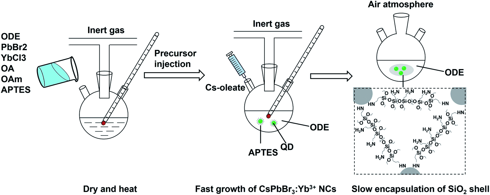
Colloidal CsPbBr3 perovskite NCs with oleylamine and oleic acid as surface ligands was synthesized using PbBr2 and Cs-oleate as precursors according to the well-established hot-injection method with a slight modification.17,18 The recipe and process for synthesis of CsPbBr3:Yb3+ NCs are the same as those used for the synthesis of CsPbBr3 NCs, except that 0.7 g of PbBr2 was replaced by 0.395 g of PbBr2 and 0.225 g of YbCl3·6H2O. The CsPbBr3:Yb3+@SiO2 NCs were prepared by a modified hot-injection method as showed in Fig. 1. All chemical, including organosilicon precursor, rare earth ion, PbBr2, Cs-oleate precursors and organic ligands were mixed in a water-free system to form perovskite NCs, and then the whole NCs system was open to the air atmosphere and the trace water vapor was captured and triggered the hydrolysis of APTES to form SiO2 shell, which greatly avoid the contact to the NCs surface.
 |
| | Fig. 1 Schematic of modified hot-injection method for preparation of CsPbBr3:Yb3+@SiO2 NCs. | |
Generally, APTES is an important organosilicon precursor for preparing silica shell or SiO2 microspheres, and also can be used to introduce amide functional group around NCs.44 In our study, APTES was chosen both as the precursor for SiO2 shell and the capping agent for the inorganic perovskite NCs. Specifically, the injection time for APTES was chosen after the complete solubilization of the PbBr2 and YbCl3 salts, but before the injection of Cs-oleate precursor. We believe that it is a very facile and important operation for fabricating of high quality SiO2-encapsulated Yb3+-doped CsPbBr3 NCs. On the one hand, the APTES is helpful for the growth of high luminescent CsPbBr3 NCs. The quick formation of monodisperse CsPbBr3 NCs takes advantages of the highly ionic nature of the chemical bonding in these compounds (from a structural standpoint, they consist of singly charged anions and exhibit highly ionic bonding). Meanwhile, APTES helps to dissolve PbBr2 and stabilize the formed NCs, and the amino group in the APTES can effectively passivate the NCs surface to maintain their original PLQYs.
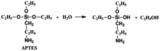
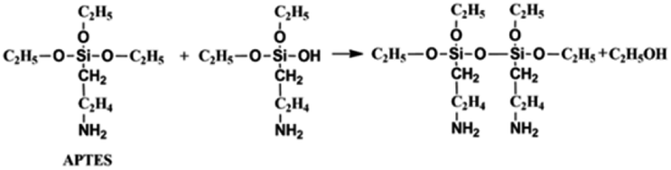
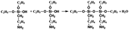
On the other hand, the APTES is beneficial for the growth of SiO2 shell around the NCs. Generally, the success of this shell protective strategy could be mainly attributed to the following two reasons. First, the APTES had been contacting the CsPbBr3 NCs during the whole crystal nucleation and growth of the NCs in inert atmosphere. Hence, the NCs surface was well protected by the APTES before exposure in an open environment. Second, once the NCs solution contact external water molecule, the three silyl ether groups in the APTES can be hydrolyzed to form a cross-linked SiO2 matrix and cover the NCs. In the whole hydrolysis process, the APTES arrested the water (H2O) molecules in air (shown in eqn (1)), and then triggered the hydrolysis of the APTES around the NCs. The Si–OC2H5 group in APTES was transformed to Si–OH (silanol); next Si–OH reacted with Si–OC2H5 group (shown in eqn (2)) or other Si–OH (shown in eqn (3)) to form Si–O–Si bond and obtain other H2O molecules. The new obtained H2O molecules would be used for further hydrolysis of APTES (shown in eqn (1)). Herein, it is very important that the H2O molecules in air initially drive hydrolysis of the triethoxysilane groups and allow the condensation among silyl ethers and silanol (Fig. 1).
| |
 | (1) |
| |
 | (2) |
| |
 | (3) |
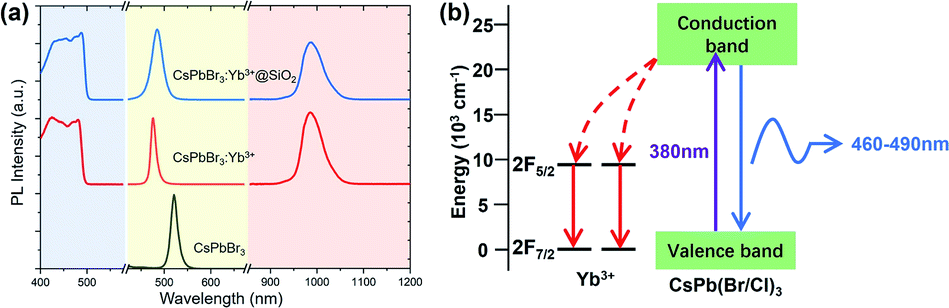
Fig. 2a shows the visible and NIR emission spectra of CsPbBr3 NCs, CsPbBr3:Yb3+ NCs, and CsPbBr3:Yb3+@SiO2 NCs pumped by a 380 nm laser source. These NCs possessed visible PL peaks of 521 nm, 476 nm and 484 nm with corresponding FWHM of 17 nm, 14 nm and 24 nm, and NIR PL peaks of 985 nm with corresponding FWHM of 34 nm and 35 nm. Their visible PLQYs were about 90% (CsPbBr3), 47% (CsPbBr3:Yb3+) and 31% (CsPbBr3:Yb3+@SiO2), respectively, and NIR PLQYs were about 44% (CsPbBr3:Yb3+) and 64% (CsPbBr3:Yb3+@SiO2), respectively. The visible emission peaks of the Yb3+ doped CsPbBr3 NCs generated blue-shift due to the substitution of Br− by Cl− ions, which enlarged the bandgap of the NCs. The small difference between CsPbBr3:Yb3+ NCs and CsPbBr3:Yb3+@SiO2 NCs is caused by the small difference in composition, as measured by ICP-OES and shown in Table 1. In the NIR region, a strong emission peak centred at 985 nm can be observed for both the naked and coated CsPbBr3:Yb3+ NCs, which originated from the 2F5/2 to 2F7/2 transition of the Yb3+ ions. The intrinsic emissions of Yb3+ ions excited by the absorption of perovskite NCs suggest an efficient energy transfer from the perovskite host to the Yb3+ ions, as depicted in Fig. 2b. Detailed studies have confirmed that the doped atoms substituted the Pb2+ ions in the lattice.45 It is also believed that because of the charge difference between Yb3+ and Pb2+, charge compensation defects VPb will be introduced,30 which exists in the form of Yb3+–VPb–Yb3+. In the process of wavelength conversion, VPb can excite the two Yb3+ ions adjacent to it, resulting in a higher PLQY. These conclusions are consistent with those in our study. For the Yb3+ ions are excited by the host NCs, the proportion of doped ions plays a very important role in quantum conversion efficiency. We have made several attempts for the ratio of YbCl3 and PbBr2, the initial PLQYs are shown in Table 2.
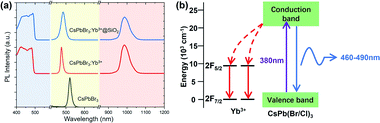 |
| | Fig. 2 (a) Excitation spectra (emission of 985 nm, left), visible PL spectra (middle), and infrared PL spectra (right) of the synthesized perovskite NCs. (b) Schematic diagram of energy transfer in the Yb3+ doped CsPbBr3 NCs. | |
Table 1 Br, Cl, and Yb contents in CsPbBr3:Yb3+ NCs and CsPbBr3:Yb3+@SiO2 NCs
| NCs |
Br (%) |
Cl (%) |
Yb (%) |
| CsPbBr3:Yb3+ NCs |
23.35 |
24.86 |
1.97 |
| CsPbBr3:Yb3+@SiO2 NCs |
29.71 |
20.37 |
1.48 |
Table 2 Initial PLQYs of CsPbBr3:Yb3+@SiO2 NCs with different doping ratio
| PbBr2:YbCl3 (mole ratio) |
Visible PLQY (%) |
NIR PLQY (%) |
| 1.3:0.54 |
48 |
43 |
| 1.2:0.64 |
41 |
52 |
| 1.1:0.74 |
31 |
64 |
| 1.0:0.84 |
35 |
38 |
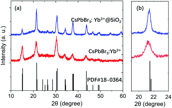
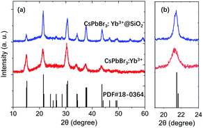
Fig. 3a–c show the TEM images of CsPbBr3, CsPbBr3:Yb3+ and CsPbBr3:Yb3+@SiO2 NCs, and the inseted are their corresponding HRTEM images. All their average sizes were about 8.4 ± 1.4 nm for CsPbBr3 NCs, 8.3 ± 1.3 nm for CsPbBr3:Yb3+ NCs and 13.5 ± 1.8 nm for CsPbBr3:Yb3+@SiO2 NCs. It can be clearly seen that the CsPbBr3 and CsPbBr3:Yb3+ NCs showed the cubic shape, and the NCs were uniformly arranged on the carbon-coated Cu grid. The (100) crystal plane distance of the CsPbBr3:Yb3+ NCs is 0.404 nm (Fig. 3b), which is slightly smaller than that of undoped CsPbBr3 NCs (0.415 nm in Fig. 3a). The slight variation in lattice constant is because of two reasons: the Yb3+ ionic possess a small radius (0.087 nm) than that of Pb2+ ions (0.119 nm),24 and the introduction of Cl− ions into the NCs by YbCl3. The X-ray diffraction (XRD) patterns (Fig. 4) show that all the NCs have the same cubic phase (PDF#18–0364), and the shift is consistent with the content of Cl−. The SiO2 shell have no effect on the crystal structure of the NCs. In Fig. 3c, we can see clearly a silica shell on the edge of the NCs with a thickness of 3–4 nm. The Fourier transform image for the selected CsPbBr3:Yb3+@SiO2 NC (Fig. 3c) shows two diffraction patterns. The spots originate from the crystal perovskite NCs, while the concentric circles reflect an amorphous coating on the surface of the NCs, which we believe to be the silica shell. Fig. 3c and d both indicate the uniform distribution of silica on the surface of the NCs.
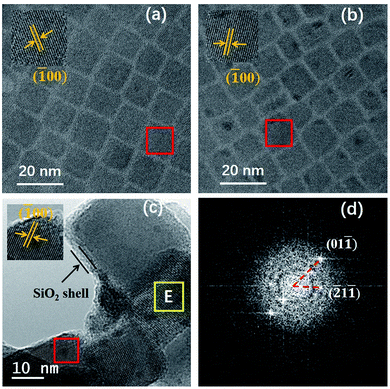 |
| | Fig. 3 (a) TEM image of CsPbBr3 NCs (8.4 nm). (b) TEM image of CsPbBr3:Yb3+ NCs (8.3 nm). (c) TEM image of CsPbBr3:Yb3+@SiO2 NCs (13.5 nm). The inseted pictures are their corresponding HRTEM images for selected NCs in red rectangle. (d) Fourier transform image for selected CsPbBr3:Yb3+@SiO2 NC in area E (c). | |
 |
| | Fig. 4 XRD patterns of CsPbBr3:Yb3+ and CsPbBr3:Yb3+@SiO2. | |
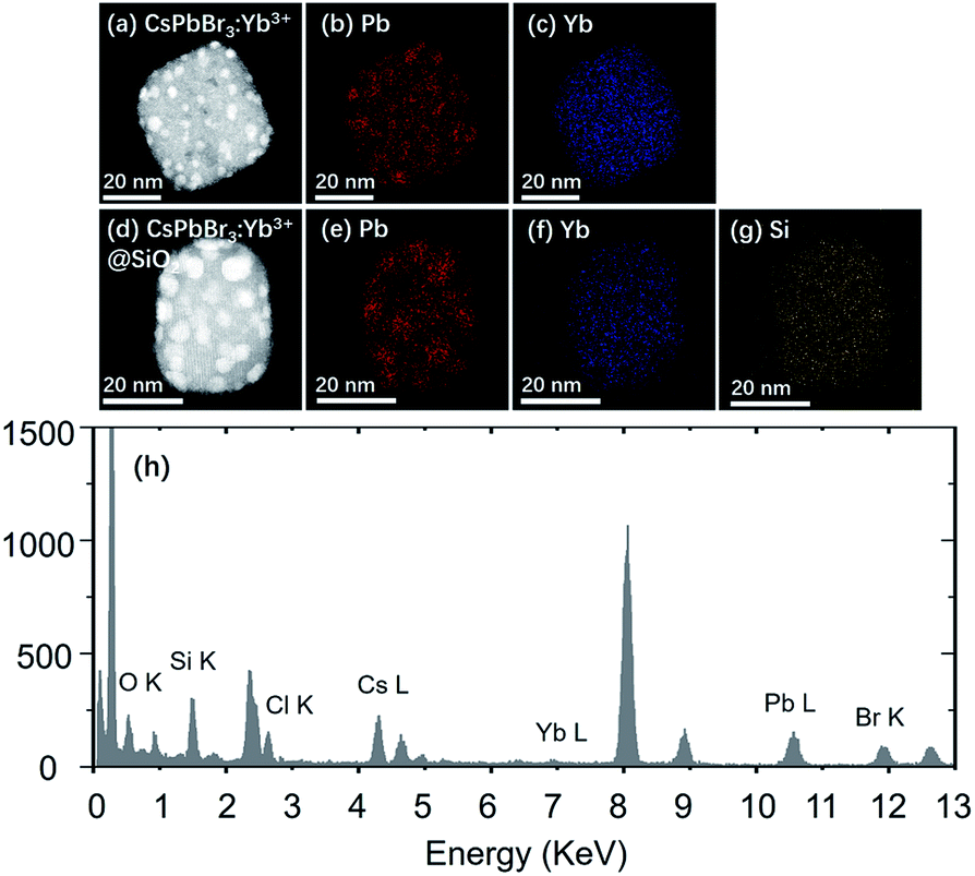
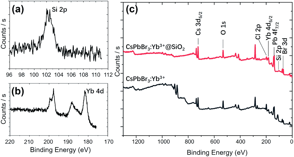
Fig. 5 shows the STEM images and element mapping images of CsPbBr3:Yb3+ NCs and CsPbBr3:Yb3+@SiO2 NCs. Fig. 5c and f demonstrate that a uniform distribution of Yb3+ is obtained, which is beneficial for high energy-transfer efficiency. The bright spots in the NCs (Fig. 5a and d) were caused by the reunion of Pb2+ ions under an electron radiation during the STEM characterization. The Si ion mapping image (Fig. 5g) also shows a uniform SiO2 coating in the CsPbBr3:Yb3+@SiO2 NCs. The EDS spectrum further reveals the presence of Yb3+ dopant and SiO2 coating in the NCs. To further verify the characterization information obtained by STEM and EDS, the XPS comparative analysis was performed for the naked and coated CsPbBr3:Yb3+ NCs (Fig. 6). As can be seen in Fig. 6c, Si was coated on the surface of CsPbBr3:Yb3+@SiO2 NCs, but not on the surface of uncoated CsPbBr3:Yb3+ NCs. The oxygen signal in both the samples may probably due to oxygen pollution during preparation and storage. It should be noted that the exist of Yb element on the surface of silica-coated NCs may be caused by a small thickness of SiO2 shell.
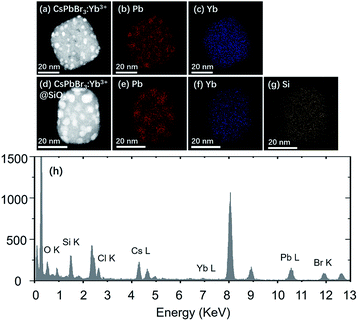 |
| | Fig. 5 (a) STEM image of CsPbBr3:Yb3+ NCs. (b and c) EDS elemental maps of Pb and Yb in the NCs shown in (a). (d) STEM image of CsPbBr3:Yb3+@SiO2 NCs. (e–g) EDS elemental maps of Pb, Yb and Si in the NCs shown in (d). (h) EDS profile of CsPbBr3:Yb3+@SiO2 NCs. | |
 |
| | Fig. 6 High-resolution XPS spectra of Si 2p (a) and Yb 4d (b) on the surface of CsPbBr3:Yb3+@SiO2 NCs. (c) XPS survey spectra of CsPbBr3:Yb3+ NCs and CsPbBr3:Yb3+@SiO2 NCs. | |
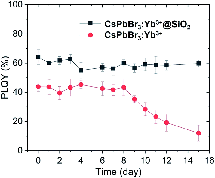
Fig. 7 shows the infrared PLQYs for the naked and coated CsPbBr3:Yb3+ NCs. The stability of the NCs improved dramatically due to the protection of silica shell from oxygen and water. As can be seen, the PLQYs of the as-prepared coated NCs were significantly higher, and the uncoated NCs decayed faster than the coated NCs did in room atmosphere with humidity of 50%. The PLQYs of the uncoated NCs started to decrease after 8 days and was about 20% after 15 days, while the PLQYs of the coated CsPbBr3:Yb3+ NCs remained constant for over 15 days. The dangling bonds on the NC surface were well passivated by SiO2 shell. Our unique fabrication technology for SiO2 shell can efficiently passivate the dangling bonds on the NCs surface, which slightly increased the initial PLQYs and further protected the NCs from environment (water and oxygen).
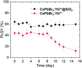 |
| | Fig. 7 Variation of infrared PLQYs of CsPbBr3:Yb3+ NCs and CsPbBr3:Yb3+@SiO2 NCs with time (emission at 985 nm, excited by 365 nm). | |
Conclusions
In summary, we have successfully developed a facile approach for fabricating SiO2-encapsulated Yb3+-doped CsPbBr3 NCs by slowly hydrolyzing the organosilicon precursor in situ. Experiment results showed that the Yb3+ ions were uniformly distributed in the NCs, and the whole NCs were completely encapsulated by a dense SiO2. The as-prepared CsPbBr3:Yb3+@SiO2 NCs can emit a strong 985 nm infrared photoluminescence, which originates from the intrinsic luminescence of Yb3+ in the perovskite NCs host, pumped by the perovskite NCs. Research results showed that the silica shell can efficiently passivate the dangling bonds on the NCs surface, which significantly increased the initial PLQYs and further protected the nanocrystals from environment (water and oxygen). The compelling combination of enhanced optical stability and environmental robustness makes the silica-coated Yb3+-doped CsPbBr3 perovskite NCs appealing for optoelectronic applications, particularly for the near-infrared spectral regions (985 nm), where typical CsPbX3 NCs suffer from serious photogradation. This method described here can be used to introduce other NCs.
Conflicts of interest
There are no conflicts to declare.
Acknowledgements
This work was financially supported by the National Natural Science Foundation of China (No. 61771024, 61627814, 61690194, and 61901009), Shenzhen Science and Technology Plan (JCYJ 20170412153729436, 20170817113844300 and 20180227175348359), Projects Foundation of YOFC (No. SKLD1708), Key Research Program of Frontier Sciences, CAS (Grant No. QYZDY-SSW-JSC022) and Postdoctoral Research Foundation of China (No. 2018M641086).
References
- M. D. Smith and H. I. Karunadasa, Acc. Chem. Res., 2018, 51, 619–627 CrossRef CAS PubMed.
- Y. Wang, X. Li, J. Song, L. Xiao, H. Zeng and H. Sun, Adv. Mater., 2015, 27, 7101–7108 CrossRef CAS PubMed.
- G. Xing, N. Mathews, S. S. Lim, N. Yantara, X. Liu, D. Sabba, M. Grätzel, S. Mhaisalkar and T. C. Sum, Nat. Mater., 2014, 13, 476 CrossRef CAS PubMed.
- J. Song, J. Li, X. Li, L. Xu, Y. Dong and H. Zeng, Adv. Mater., 2015, 27, 7162–7167 CrossRef CAS PubMed.
- P. Cai, X. Wang, H. J. Seo and X. Yan, Appl. Phys. Lett., 2018, 112, 153901 CrossRef.
- H. Wu, Y. Zhang, X. Zhang, M. Lu, C. Sun, T. Zhang and W. W. Yu, Adv. Opt. Mater., 2017, 5, 1700377 CrossRef.
- P. Wang, X. Bai, C. Sun, X. Zhang, T. Zhang and Y. Zhang, Appl. Phys. Lett., 2016, 109, 063106 CrossRef.
- X. Y. Chin, A. Perumal, A. Bruno, N. Yantara, S. A. Veldhuis, L. Martínez-Sarti, B. Chandran, V. Chirvony, A. S.-Z. Lo and J. So, Energy Environ. Sci., 2018, 11, 1770–1778 RSC.
- Y. H. Kim, H. Cho, J. H. Heo, T. S. Kim, N. Myoung, C. L. Lee, S. H. Im and T. W. Lee, Adv. Mater., 2015, 27, 1248–1254 CrossRef CAS PubMed.
- M. A. Green, A. Ho-Baillie and H. J. Snaith, Nat. Photon., 2014, 8, 506 CrossRef CAS.
- Z. Wang, Z. Shi, T. Li, Y. Chen and W. Huang, Angew. Chem., Int. Ed., 2017, 56, 1190–1212 CrossRef CAS PubMed.
- Y. Dong, Y. Gu, Y. Zou, J. Song, L. Xu, J. Li, J. Xue, X. Li and H. Zeng, Small, 2016, 12, 5622–5632 CrossRef CAS PubMed.
- Y. Ling, Y. Tian, X. Wang, J. C. Wang, J. M. Knox, F. Perez-Orive, Y. Du, L. Tan, K. Hanson and B. Ma, Adv. Mater., 2016, 28, 8983–8989 CrossRef CAS PubMed.
- X. Li, D. Yu, F. Cao, Y. Gu, Y. Wei, Y. Wu, J. Song and H. Zeng, Adv. Funct. Mater., 2016, 26, 5903–5912 CrossRef CAS.
- Y.-H. Kim, G.-H. Lee, Y.-T. Kim, C. Wolf, H. J. Yun, W. Kwon, C. G. Park and T.-W. Lee, Nano Energy, 2017, 38, 51–58 CrossRef CAS.
- Q. A. Akkerman, V. D'Innocenzo, S. Accornero, A. Scarpellini, A. Petrozza, M. Prato and L. Manna, J. Am. Chem. Soc., 2015, 137, 10276–10281 CrossRef CAS PubMed.
- G. Nedelcu, L. Protesescu, S. Yakunin, M. I. Bodnarchuk, M. J. Grotevent and M. V. Kovalenko, Nano Lett., 2015, 15, 5635–5640 CrossRef CAS PubMed.
- L. Protesescu, S. Yakunin, M. I. Bodnarchuk, F. Krieg, R. Caputo, C. H. Hendon, R. X. Yang, A. Walsh and M. V. Kovalenko, Nano Lett., 2015, 15, 3692–3696 CrossRef CAS PubMed.
- F. Hu, C. Yin, H. Zhang, C. Sun, W. W. Yu, C. Zhang, X. Wang, Y. Zhang and M. Xiao, Nano Lett., 2016, 16, 6425–6430 CrossRef CAS PubMed.
- S. C. Erwin, L. Zu, M. I. Haftel, A. L. Efros, T. A. Kennedy and D. J. Norris, Nature, 2005, 436, 91–94 CrossRef CAS PubMed.
- F. Wang, Y. Han, C. S. Lim, Y. Lu, J. Wang, J. Xu, H. Chen, C. Zhang, M. Hong and X. Liu, Nature, 2010, 463, 1061–1065 CrossRef CAS PubMed.
- C. Li, X. Lu, W. Ding, L. Feng, Y. Gao and Z. Guo, Acta Crystallogr., Sect. B: Struct. Sci., 2008, 64, 702–707 CrossRef CAS PubMed.
- W. Travis, E. Glover, H. Bronstein, D. Scanlon and R. Palgrave, Chem. Sci., 2016, 7, 4548–4556 RSC.
- L. Zhou, T. Liu, J. Zheng, K. Yu, F. Yang, N. Wang, Y. Zuo, Z. Liu, C. Xue and C. Li, J. Phys. Chem. C, 2018, 122, 26825–26834 CrossRef CAS.
- A. K. Guria, S. K. Dutta, S. D. Adhikari and N. Pradhan, ACS Energy Lett., 2017, 2, 1014–1021 CrossRef CAS.
- W. Van der Stam, J. J. Geuchies, T. Altantzis, K. H. Van Den Bos, J. D. Meeldijk, S. Van Aert, S. Bals, D. Vanmaekelbergh and C. de Mello Donega, J. Am. Chem. Soc., 2017, 139, 4087–4097 CrossRef CAS PubMed.
- M. Lu, X. Zhang, X. Bai, H. Wu, X. Shen, Y. Zhang, W. Zhang, W. Zheng, H. Song and W. W. Yu, ACS Energy Lett., 2018, 3, 1571–1577 CrossRef CAS PubMed.
- D. Zhou, D. Liu, G. Pan, X. Chen, D. Li, W. Xu, X. Bai and H. Song, Adv. Mater., 2017, 29, 1704149 CrossRef PubMed.
- X. Li, S. Duan, H. Liu, G. Chen, Y. Luo and H. Ågren, J. Phys. Chem. Lett., 2019, 10, 487–492 CrossRef PubMed.
- T. J. Milstein, D. M. Kroupa and D. R. Gamelin, Nano Lett., 2018, 18, 3792–3799 CrossRef CAS PubMed.
- X. Zhang, Y. Zhang, X. Zhang, W. Yin, Y. Wang, H. Wang, M. Lu, Z. Li, Z. Gu and W. Y. William, J. Mater. Chem. C, 2018, 6, 10101–10105 RSC.
- G. Pan, X. Bai, D. Yang, X. Chen, P. Jing, S. Qu, L. Zhang, D. Zhou, J. Zhu and W. Xu, Nano Lett., 2017, 17, 8005–8011 CrossRef CAS.
- J. De Roo, M. Ibáñez, P. Geiregat, G. Nedelcu, W. Walravens, J. Maes, J. C. Martins, I. Van Driessche, M. V. Kovalenko and Z. Hens, ACS Nano, 2016, 10, 2071–2081 CrossRef CAS PubMed.
- F. Liu, Y. Zhang, C. Ding, S. Kobayashi, T. Izuishi, N. Nakazawa, T. Toyoda, T. Ohta, S. Hayase and T. Minemoto, ACS Nano, 2017, 11, 10373–10383 CrossRef CAS.
- S. Huang, Z. Li, L. Kong, N. Zhu, A. Shan and L. Li, J. Am. Chem. Soc., 2016, 138, 5749–5752 CrossRef CAS.
- Z. Li, L. Kong, S. Huang and L. Li, Angew. Chem., Int. Ed., 2017, 56, 8134–8138 CrossRef CAS PubMed.
- H. C. Wang, S. Y. Lin, A. C. Tang, B. P. Singh, H. C. Tong, C. Y. Chen, Y. C. Lee, T. L. Tsai and R. S. Liu, Angew. Chem., Int. Ed., 2016, 55, 7924–7929 CrossRef CAS PubMed.
- C. Sun, Y. Zhang, C. Ruan, C. Yin, X. Wang, Y. Wang and W. W. Yu, Adv. Mater., 2016, 28, 10088–10094 CrossRef CAS PubMed.
- M. Meyns, M. Perálvarez, A. Heuer-Jungemann, W. Hertog, M. Ibáñez, R. Nafria, A. Genç, J. Arbiol, M. V. Kovalenko and J. Carreras, ACS Appl. Mater. Interfaces, 2016, 8, 19579–19586 CrossRef CAS PubMed.
- F. Palazon, F. Di Stasio, Q. A. Akkerman, R. Krahne, M. Prato and L. Manna, Chem. Mater., 2016, 28, 2902–2906 CrossRef CAS PubMed.
- J. Yang, B. D. Siempelkamp, D. Liu and T. L. Kelly, ACS Nano, 2015, 9, 1955–1963 CrossRef CAS PubMed.
- J. Liu, L. Zhang, Q. Yang and C. Li, Microporous Mesoporous Mater., 2008, 116, 330–338 CrossRef CAS.
- F. Di Stasio, S. Christodoulou, N. Huo and G. Konstantatos, Chem. Mater., 2017, 29, 7663–7667 CrossRef.
- D. Franke, D. K. Harris, L. Xie, K. F. Jensen and M. G. Bawendi, Angew. Chem., Int. Ed., 2015, 54, 14299–14303 CrossRef CAS PubMed.
- W. van der Stam, J. J. Geuchies, T. Altantzis, K. H. W. van den Bos, J. D. Meeldijk, S. Van Aert, S. Bals, D. Vanmaekelbergh and C. d. M. Donega, J. Am. Chem. Soc., 2017, 139, 4087–4097 CrossRef CAS PubMed.
|
| This journal is © The Royal Society of Chemistry 2020 |
Click here to see how this site uses Cookies. View our privacy policy here. 
 Open Access Article
 This Open Access Article is licensed under a Creative Commons Attribution-Non Commercial 3.0 Unported Licence
 a,
Aidi Zhangb,
Taoran Liuc,
Lin Zhou
a,
Aidi Zhangb,
Taoran Liuc,
Lin Zhou