
 Open Access Article
 This Open Access Article is licensed under a Creative Commons Attribution-Non Commercial 3.0 Unported Licence
Ratiometric temperature measurement using negative thermal quenching of intrinsic BiFeO3 semiconductor nanoparticles†
Željka Antić *a,
K. Prashanthi*b,
Sanja Kuzmana,
Jovana Perišaa,
Zoran Ristića,
V. R. Palkarc and
Miroslav D. Dramićanina
*a,
K. Prashanthi*b,
Sanja Kuzmana,
Jovana Perišaa,
Zoran Ristića,
V. R. Palkarc and
Miroslav D. Dramićanina
aUniversity of Belgrade, Vinča Institute of Nuclear Sciences, P.O. Box 522, Belgrade, Serbia. E-mail: zeljkaa@gmail.com
bUniversity of Alberta, Department of Chemical & Materials Engineering, Edmonton, Canada. E-mail: kovur@ualberta.ca
cIndian Institute of Technology Bombay (IIT-B), Mumbai, India
First published on 30th April 2020
Abstract
A strategy for optical nanothermometry using the negative thermal quenching behavior of intrinsic BiFeO3 semiconductor nanoparticles has been reported here. X-ray diffraction measurement shows polycrystalline BiFeO3 nanoparticles with a rhombohedral distorted perovskite structure. Transmission electron microscopy shows agglomerated crystalline nanoparticles around 20 nm in size. Photoluminescence measurements show that intensity of the defect level emission increases significantly with temperature, while the intensity of near band emission and other defect levels emissions show an opposite trend. The most important figures of merit for luminescence nanothermometry: the absolute (Sa) and the relative sensor sensitivity (Sr) and the temperature resolution (ΔTm) were effectively resolved and calculated. The relative sensitivity and temperature resolution values are found to be 2.5% K−1 and 0.2 K, respectively which are among the highest reported values observed so far for semiconductors.
Introduction
For 80% of all sensors on the global market, temperature is the most frequently measured physical quantity. Many types of thermometers are currently being used including thermocouples, thermistors, liquid-in-glass, bimetallic, resistance, manometric and infrared thermometers.1,2Scientific and technological progress creates an ongoing need for the development of new measuring concepts and instruments. There is now an immediate need for non-contact thermometry of moving or contact-sensitive objects, bodies that are difficult to access or in hazardous locations. Temperature measurements resulting from changes in materials' optical properties are considered as a promising route to meet the needs. Raman scattering, optical interferometry, thermoreflectance, near-field scanning optical microscopy and photoluminescence (PL) spectroscopy are the optical methods of interest.1
Temperature strongly affects photoluminescence features of optical materials such as peak energy and intensity, band shape, excited states lifetimes, and rise-times, which can be exploited to measure temperature. The temperature read-out method most commonly used in the present practice of luminescence thermometry is one based on the determination of the ratio of intensities of different emission bands of luminescent material. Ratiometric measurements are self-referencing and prone to fluctuations in excitation sources and detection electronics.1
To date, luminescence-based nanothermometry has been performed mainly using organic dyes, lanthanides (Ln) and transition metal (TM)-doped nanoparticles, and semiconductor quantum dots (QDs). In recent years researchers have started to explore the potential of luminescent materials' negative thermal quenching effect for non-contact temperature sensing. Lei et al. showed in a series of NaGdF4@Ca/Yb/Er:NaGdF4 core–shell nanocrystals that confining doping ions in two-dimensional space and introducing defect energy level via low-valence doping benefit the negative thermal quenching effect in the upconversion nanocrystals.3 Zou et al. reported a strategy for enhancing photon upconversion at high temperatures by taking advantage of negative thermal expansion host materials. They reported a 29-fold enhancement of green upconversion luminescence in the Er3+-doped orthorhombic Yb2W3O12 crystals when temperature is increased from 303 to 573 K.4 Also, authors have focused on uncommon thermal quenching effects in thermochromic materials and Covalent Organic Frameworks (COF). Mazza et al. have shown that the spontaneous opening and closing of oxazine heterocycles might become a viable mechanism to design fluorescence sensors capable of responding ratiometrically to temperature.5 Kaczmarek et al. have proposed a new class of materials, Ln3+-grafted Covalent Organic Frameworks (LnCOF), employed for temperature sensing applications. In Eu/Tb systems they observed a quite unusual and rarely reported behavior in which there is no thermal quenching of the Tb3+ emission, as a result of the absence of ion-to-ligand/host energy back transfer.6
In semiconductors, the intensity of photoluminescence normally decreases with higher temperature (thermal quenching) mainly due to thermally-induced delocalization of charge carriers followed by non-fluorescent trapping.7,8 Here, an approach for monitoring temperature variations using defect emission from intrinsic semiconductor BiFeO3 (BFO) nanoparticles (NPs) is reported. Generally, materials made up of nanoparticles have a larger surface area when compared to the same volume of material made up of larger particles. It means that the surface-to-volume ratio increases as the radius of the sphere decreases. In BFO nanostructures, surface states play a vital role in optical and electrical characteristics due to the high surface-to-volume ratio when compared with bulk material.9–12 They serve as traps for carriers and hence affect the recombination and transport of charge carriers.13–16 Unlike conventional optical thermometry with semiconductors where luminescent signal decreases at high temperatures, we have observed that BFO NPs exhibit an emission-related negative thermal quenching (NTQ), where the photoluminescence intensity increases with temperature. Here, we propose strategy for temperature sensing based on the NTQ mechanism of intrinsic BFO NPs with an excellent performance of thermal sensitivity and resolution.
Experimental part
Materials
Bismuth(III) nitrate pentahydrate (98%) and 2-methoxyethanol (99+%) were purchased from Acros Organics and used as received. Ferric nitrate nonahydrate (99.99%) was purchased from Sigma Aldrich and used as received.Preparation of semiconductor BFO NPs
Semiconductor BFO NPs were prepared via sol–gel route. BFO solution (sol) has been prepared by mixing bismuth(III) nitrate pentahydrate and ferric(III) nitrate nonahydrate in a molar ratio of 1.05![[thin space (1/6-em)]](https://www.rsc.org/images/entities/char_2009.gif) :1 in 2-methoxyethanol as a solvent. The precursor solution was stirred at 80 °C for one hour, after which a reddish sol was recovered. The solution was dried at 100 °C for 2 h in vacuum to obtain BFO xerogel powder which was then ground in a crucible, and annealed at 600 °C for 2 h in the air.
:1 in 2-methoxyethanol as a solvent. The precursor solution was stirred at 80 °C for one hour, after which a reddish sol was recovered. The solution was dried at 100 °C for 2 h in vacuum to obtain BFO xerogel powder which was then ground in a crucible, and annealed at 600 °C for 2 h in the air.
Characterization
The size of the BFO NPs was analysed using transmission electron microscopy (TEM) (JEOL JEM-2100).Structural analysis of BFO NPs was done by X-ray diffraction measurements on a Rigaku X-ray diffractometer using Cu Kα radiation (λ = 1.546 Å).
The PL thermometry data were collected using a Fluorolog-3 Model FL3-221 spectrofluorometer system (Horiba-Jobin-Yvon) over the temperature range from room temperature (RT = 293 K) to 453 K under continuous excitation using 450 W xenon lamp (λex = 320 nm). Time-resolved PL measurements were acquired utilizing a Xenon–Mercury pulsed lamp as excitation source. For PL measurements, the BFO NPs were prepared in a form of pallet. The BFO NPs pallet was placed on a custom-made temperature controlled furnace, and emission spectra were collected via an optical fiber bundle. The temperature of the samples was controlled within the accuracy of ±0.5 K by a temperature control system utilizing a proportional-integral-derivative feedback loop equipped with the T-type thermocouple for temperature monitoring.
Results and discussion
Morphological and structural characterization of BFO NPs
Transmission electron microscopy shows agglomerated crystalline nanoparticles with variable dimensions in 10–50 nm range and boundary lines observed clearly in some regions (Fig. 1(a)). Fig. 1(b) depicts a TEM image of a single BFO NPs around 20 nm in size. The interplanar spacing observed from Fig. 1(c) is about 0.374 nm for (012) and 0.278 nm for (104) planes. The obtained lattice spacing is in a close agreement with the literature values for BFO nanostructures.17,18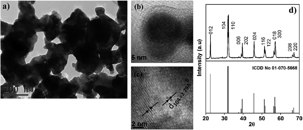 | ||
| Fig. 1 (a) Low-magnification TEM image of a region with agglomerated BFO NPs; (b) HRTEM image of single nanoparticle; (c) high resolution TEM showing lattices spacing of BFO NPs and (d) XRD pattern of BFO NPs presented with corresponding ICDD card No. 01-070-5668. | ||
The XRD pattern, Fig. 1(d), corresponds to polycrystalline BFO of the R3C rhombohedral distorted perovskite structure (ICDD 01-070-5668), and no noticeable diffractions can be observed for impurity phases. The average crystallite size of ∼30 nm was estimated from the full widths at half maximum (FWHMs) of the resolved reflections in the X-ray powder diffraction pattern using the Debay-Scherrer approximation. A Scherrer constant of K = 0.89 was taken as an average for every reflection although it was shown that this constant is anisotropic and its value may vary for different (hkl).19
One should note that the X-ray diffraction is a structural technique that provides the analysis at a micron scale, while the TEM reveals the structure and morphology at the atomic level (Fig. 1(c)). Therefore, the calculated average crystallite size of ∼30 nm from the XRD is in agreement with the 10 to 50 nm particle size obtained from TEM measurements.
By preparing the material with no traces of impurity phases, one can be ascertain in the reproducibility of photoluminescent measurements and, therefore, in the usability of the material as a luminescent thermal probe.
Temperature dependant BFO emission
Fig. 2 shows schematic illustration of used experimental setup and BFO NPs photoluminescence spectra obtained with increasing temperature from room to 453 K. Emission band with maxima at 482 nm (E1) corresponds to band edge/near band emission (NBE), while maxima at 523 nm (E2), 544 nm (E3) and 551 nm (E4) correspond to the defect level/surface state emissions (DLE). The emissions at 523 nm, 544 nm, and 551 nm are associated with oxygen vacancies (VO) presence (more details are available in ESI, XPS, Fig. S1†).10,11,20 The intensity of the defect level emission E2 (523 nm) increases significantly with temperature, while the intensity of near band emission E1 (482 nm) and other defect levels (E3, E4) emissions show an opposite trend (Fig. 3(A)). The intensity of the defect level emission E2 (523 nm) increases significantly with temperature, while the intensity of near band emission E1 (482 nm) and other defect levels (E3, E4) emissions show an opposite trend (Fig. 3(A)). The difference in the temperature dependence of band edge/near band (E1) and defect level/surface state (E2, E3, E4) emissions causes the change of probe's emission color from pale blue to light green, as shown in CIE color diagram in Fig. 3(B).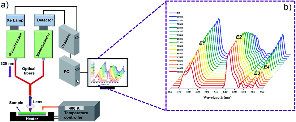 | ||
| Fig. 2 (a) Experimental setup used for optical nanothermometry and (b) enlarged PL spectra of BFO nanoparticles over 293–453 K temperature range (temperature increment 10 K). | ||
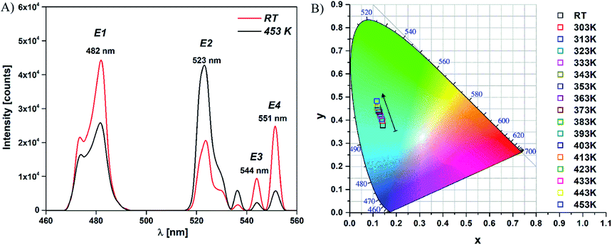 | ||
| Fig. 3 (A) PL emission spectra of BFO NPs at RT (293 K) and at 453 K (λex = 320 nm) and (B) CIE diagram of the BFO NPs in the RT – 453 K temperature range. | ||
Oxygen vacancy related defect emissions and NTQ behavior has been reported in some oxide systems.20–27 Moreover, in our previously published work on multifferoic BFO nanowires (NWs) reasonable interpretation of the photoluminescence NTQ process in BFO NWs and detailed representation of the energy levels and E1, E2, E3, and E4 bands is given.15 Briefly, according to the multi-level model developed by Shibata28 temperature dependent PL intensity can be expressed by activation energy for the process that increases the PL intensity with increasing temperature – NTQ  and activation energy for the non-radiative channels
  . The activation energies of NTQ process
  in BFO nanowires were found to be a few times greater for E2 than for E1, E3, and E4. Therefore, as temperature increases, the carriers with lower activation energy will start to escape into the barrier where they can recombine non-radiatively leading to decrease in the PL intensity while carriers with higher activation energy lead to NTQ behavior. In addition to recombination, one should note that energy states are closely spaced in energy so, according to Boltzmann distribution, redistribution of electron population between states exists and is higher at higher temperature (being proportional to kT). The E2 emission comes from the trap state of highest energy which is thermally coupled to lower E3 and E4 energy state. The increase in temperature is followed by a redistribution of electrons between the traps so that high-energy trap (E2) increases in population on account of lower-energy traps (E3 and E4).
Temperature dependent luminescence decay lifetime
Due to the fact that the transitions from surface states are forbidden, the emission rate is slow and characterized by relatively high decay time (∼170 μs). Fig. 4 presents calculated lifetime values of the E2 emission as a function of temperature. Similar to BFO NWs, the lifetime is independent of the temperature change, resembling the static quenching behavior and can be explained in terms of multiple trapping and de-trapping process.15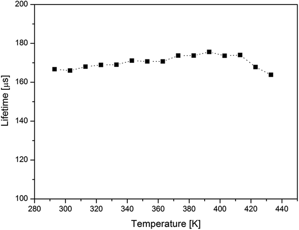 | ||
| Fig. 4 Calculated lifetime values of the E2 emission as a function of temperature. | ||
Temperature sensing based on ratiometric method
Since BFO NPs provide multiple emission peaks, a ratiometric approach to luminescence thermometry could be used. Such ratiometric measurements are insensitive to fluctuations of excitation source light or other changes in measurement conditions and, therefore, act as self-referencing (i.e., measurements do not have to be referenced with any temperature standard).1 Fig. 5(A) shows maximum PL intensity as a function of temperature for all four transitions while Fig. 5(B) shows a plot of the temperature dependence of the fluorescence intensity ratio (FIR) obtained as a ratio of E2 emission with other three (E1, E3, and E4).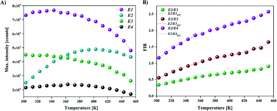 | ||
| Fig. 5 (A) Maximum PL intensities as a function of temperature for all four transitions (E1, E2, E3, E4) and (B) fluorescence intensity ratio (FIR) values of BFO NPs as a function of temperature. FIR values were obtained as the ratio between peak intensities for E1, E3 and E4 with respect to E2. | ||
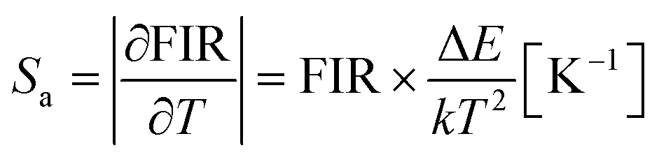
The most important figures of merits for luminescence nanothermometry are: the absolute sensor sensitivity, Sa, defined as the slope of the signal change with temperature; the relative sensor sensitivity, Sr, defined as the normalized absolute sensor sensitivity with respect to the measured value and the temperature resolution (ΔTm) indicating the minimum temperature that can be effectively resolved (where σ represents the uncertainty of the FIR measurement, here 0.5):29
 | (1) |
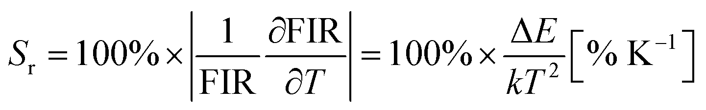 | (2) |
 | (3) |
The absolute and relative sensitivities of BFO NPs, as well as temperature resolution calculated from eqn (1)–(3) are plotted in Fig. 6 and summarized in Table 1. The maximal value of the relative sensitivity of 2.5% K−1 is found at room temperature for E2/E3 ratio and the value decreases with temperature to 0.4% K−1 at 398 K. Relative sensitivities achieved with BFO NPs are among the highest recorded for semiconductor nanothermometers, but with larger measurement range (for a comparison see Table 2).
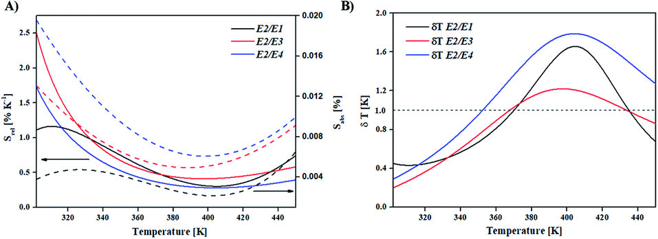 | ||
| Fig. 6 (A) Relative (solid line) and absolute (dashed line) sensitivity of FIR thermometry and (B) temperature resolution. | ||
| FIR ratio | Temperature range; Tm (K) | Thermal sensitivity | Temperature resolution | |
|---|---|---|---|---|
| Sa (K−1) | Sr (% K−1) | @ 293 K (K) | ||
| E2/E1 | 293–453 (293) | 7.4 × 10⁻³ | 1.1 | 0.45 |
| E2/E3 | 293–453 (293) | 1.3 × 10⁻² | 2.5 | 0.2 |
| E2/E4 | 293–453 (293) | 2 × 10⁻² | 1.7 | 0.3 |
| Semiconductor material/form | T range (ΔT, K) with the T at which Sr is maximum (Tm, K) | Relative sensitivity (Sr, % K−1) | Resolution (K) | Reference |
|---|---|---|---|---|
| CdSe/NCs | 82–280 | 0.44 | 8 | |
| ZnS-caped CdSe/anodized-aluminum paint QDs | 100–500 (245) | 1.3 | 30 | |
| CdSe–ZnS/QDs | 287–316 | 1.6 | 0.3 | 31 |
| CdSe–ZnS/QDs | 278–313 | 1.3 | 32 | |
| ZnS–AgInS/NPs | 293–353 | 1 | 33 | |
| CdSe/ZnS and CdTe/ZnS/QDs | 287–320 (320) | 0.9 | 34 | |
| CdTe@NaCl/QDs | 80–360 (199) | 0.61 | 35 | |
| BiFeO3/NPs | 293–453 (293) | 2.5 | 0.2 | Present work |
Estimated temperature resolutions (see Fig. 6(B)) were better than 1 K for all ratios and temperatures up to 350 K with 0.2 K maximal resolution at room temperature for E2/E3 ratio. Note that temperature resolution estimates were based on the standard deviation of measurements obtained from the equipment described in the experimental section. In practice, the resolution will depend on the used instruments and the measurement conditions.
Conclusion
In conclusion, we have investigated negative thermal quenching of intrinsic BFO NPs. Multiple peaks in the emission spectrum of BFO NPs enables the use of ratiometric luminescence thermometry in the 293–453 K temperature range with the relative sensitivity 2.5% K−1 and temperature resolution of 0.2 K at room temperature which are higher than previously reported values observed for other semiconductor nanothermometers. Unlike conventional optical thermometry with semiconductors, negative thermal quenching of BFO NPs offers a new opportunity for developing temperature sensors with superior performance at higher temperatures.Conflicts of interest
There are no conflicts to declare.Acknowledgements
The authors from Vinča Institute of Nuclear Sciences acknowledge funding from the European Union's Horizon 2020 FET Open Program under grant agreement No. 801305, and from the Ministry of Education, Science and Technological Development of the Republic of Serbia.Notes and references
- M. Dramićanin, Luminescence thermometry: methods, materials, and applications, Woodhead Publishing, Cambridge, 1st edn, 2018 Search PubMed.
- P. R. N. Childs, Practical temperature measurement, Oxford: Butterworth–Heinemann, Oxford, 2001, p. 372 Search PubMed.
- L. Lei, J. Xia, Y. Cheng, Y. Wang, G. Bai, H. Xia and S. Xu, J. Mater. Chem. C, 2018, 6, 11587–11592 RSC.
- H. Zou, X. Yang, B. Chen, Y. Du, B. Ren, X. Sun, X. Qiao, Q. Zhang and F. Wang, Angew. Chem., Int. Ed., 2019, 58, 1–6 CrossRef PubMed.
- M. M. A. Mazza, F. Cardano, J. Cusido, J. D. Baker, S. Giordani and F. M. Raymo, Chem. Commun., 2019, 55, 1112–1115 RSC.
- A. M. Kaczmarek, Y. Y. Liu, M. K. Kaczmarek, H. Liu, F. Artizzu, L. D. Carlos and P. Van Der Voort, Angew. Chem., Int. Ed., 2020, 59, 1932–1940 CrossRef CAS PubMed.
- D. J. Garcia and J. G. Sole, Quantum dot fluorescence thermometry, in Thermometry at the nanoscale: techniques and selected applications, ed. L. D. Carlos and F. Palacio, RSC Nanosci. Nanotechnol., 2016, pp. 83–123 Search PubMed.
- L. Jethi, M. M. Krause and P. Kambhampati, J. Phys. Chem. Lett., 2015, 6, 718–721 CrossRef CAS PubMed.
- K. Prashanthi, A. Phani and T. Thundat, Resonator, Nano Lett., 2015, 15, 5658–5663 CrossRef CAS PubMed.
- K. Prashanthi, G. Thakur and T. Thundat, Surf. Sci., 2012, 606, L83–L86 CrossRef CAS.
- K. Prashanthi, R. Gaikwad and T. Thundat, Nanotech, 2013, 24, 505710–505715 CrossRef PubMed.
- K. Prashanthi, P. Dhandharia, N. Miriyala, R. Gaikwad, D. Barlage and T. Thundat, Nano Energy, 2015, 13, 240–248 CrossRef CAS.
- J. Lagowski, C. L. Balestra and H. C. Gatos, Surf. Sci., 1972, 29, 213–229 CrossRef CAS.
- H. C. Gatos and J. Lagowski, J. Vac. Sci. Technol., 1973, 10, 130–135 CrossRef CAS.
- K. Prashanthi, Ž. Antić, G. Thakur, M. D. Dramićanin and T. Thundat, Phys. Status Solidi RRL, 2017, 1700352–1700356 Search PubMed.
- J. M. Moison and M. Bensoussan, Rev. Phys. Appl., 1987, 22, 293–297 CrossRef CAS.
- T. J. Park, G. C. Papaefthymiou, A. J. Viescas, A. R. Moodenbaugh and S. S. Wong, Nano Lett., 2007, 7, 766–772 CrossRef CAS PubMed.
- F. Huang, Z. Wang, X. Lu, J. Zhang, K. Min, W. Lin, R. Ti, T. T. Xu, J. He, C. Yue and J. Zhu, Sci. Rep., 2013, 3, 2907 CrossRef PubMed.
- J. I. Langford and A. J. C. Wilson, J. Appl. Crystallogr., 1978, 11, 102–113 CrossRef CAS.
- H. He, Y. Wang, J. Wang and Z. Ye, Phys. Chem. Chem. Phys., 2011, 13, 14902–14905 RSC.
- H. He, Z. Ye, S. Lin, B. Zhao, J. Huang and H. Tang, J. Phys. Chem. C, 2008, 112, 14262–14265 CrossRef CAS.
- M. Watanabe, M. Sakai, H. Shibata, C. Satou, S. Satou, T. Shibayama, H. Tampo, A. Yamada, K. Matsubara, K. Sakurai, S. Ishizuka, S. Niki, K. Maeda and I. Niikura, Phys. B, 2006, 376–377, 711–714 CrossRef CAS.
- Y. L. Zhao, Y. Sun, L. Q. Pan, K. S. Li and D. B. Yu, Appl. Phys. Lett., 2013, 102, 042404–042407 CrossRef.
- W. K. Choi, C. Park, B. Angadi, Y. S. Jung and J. W. Choi, J. Electroceram., 2009, 23, 331–334 CrossRef CAS.
- A. B. Djurišić and Y. H. Leung, Small, 2006, 2, 944–961 CrossRef PubMed.
- S. F. Wuister, A. van Houselt, D. C. de Mello, D. Vanmaekelbergh and A. Meijerink, Angew. Chem., 2004, 43, 3029–3033 CrossRef CAS PubMed.
- S. F. Wuister, D. C. de Mello and A. Meijerink, J. Am. Chem. Soc., 2004, 126, 10397–10402 CrossRef CAS PubMed.
- H. Shibata, Jpn. J. Appl. Phys., Part 1, 1998, 37, 550 CrossRef CAS.
- M. Quintanilla, A. Benayas, R. Naccache and F. Vetrone, Luminescent nanothermometry with lanthanide-doped nanoparticles, in Thermometry at the nanoscale: techniques and selected applications, ed. L. Carlos and F. Palacio, RSC Nanosci. Nanotechnol., 2016, pp. 124–166 Search PubMed.
- H. Sakaue, A. Aikawa and Y. Iijama, Sens. Actuators, B, 2010, 150, 569–573 CrossRef CAS.
- P. A. S. Jorge, M. Mayeh, R. Benrashid, P. Caldas, J. L. Santos and F. Farahi, Meas. Sci. Technol., 2006, 17, 1032–1038 CrossRef CAS.
- G. W. Walker, V. C. Sundar, C. M. Rudzinski, A. W. Wun, M. G. Bawendi and D. G. Nocera, Appl. Phys. Lett., 2003, 83, 3555–3557 CrossRef CAS.
- Y. Matsuda, T. Torimoto, T. Kameya, T. Kameyama, S. Kuwabata, H. Yamaguchi and T. Niimi, Sens. Actuators, B, 2013, 176, 505–508 CrossRef CAS.
- C. D. S. Brites, P. P. Lima, N. J. O. Silva, A. Millan, V. S. Amaral, F. Palacio and L. D. Carlos, Nanoscale, 2012, 4, 4799–4829 RSC.
- S. Kalytchuk, O. Zhovtiuk, S. V. Kershaw, R. Zboril and A. L. Rogach, Small, 2016, 12, 466–476 CrossRef CAS PubMed.
Footnote |
| † Electronic supplementary information (ESI) available. See DOI: 10.1039/d0ra01896a |
| This journal is © The Royal Society of Chemistry 2020 |