
 Open Access Article
 This Open Access Article is licensed under a Creative Commons Attribution-Non Commercial 3.0 Unported Licence
Simultaneous tuning of optical and electrical properties in a multifunctional LiNbO3 matrix upon doping with Eu3+ ions†
Nimai Pathak *a,
Partha Sarathi Ghoshb,
Sumanta Mukherjeec and
Balaji Prasad Mandald
*a,
Partha Sarathi Ghoshb,
Sumanta Mukherjeec and
Balaji Prasad Mandald
aRadiochemistry Division, Bhabha Atomic Research Centre, Mumbai, 400085, India. E-mail: nmpathak4@gmail.com; nimai@barc.gov.in; Fax: +91-22-25405151; Tel: +91-22-25590715 ext. 0636
bGlass and Advanced Materials Division, Bhabha Atomic Research Centre, Mumbai, 400085, India
cFuel Chemistry Division, Bhabha Atomic Research Centre, Mumbai, 400085, India
dChemistry Division, Bhabha Atomic Research Centre, Mumbai, 400085, India
First published on 21st August 2020
Abstract
Combined photoluminescence (PL) and dielectric studies have been carried out on both undoped and Eu3+ doped LiNbO3 compounds for their potential application in optical–electrical integration for the first time. Special focus has been given to simultaneously tuning both these physical properties. A PL study reveals that the blank compound is a blue emitting material, while upon doping with Eu3+ ions, the emitting color can be tuned from blue to red upon changing the excitation wavelength. Interestingly, the electrical property measurement of this ferroelectric compound showed that upon doping with Eu3+ ions, the remnant polarization was increased significantly. Density Functional Theory (DFT) based calculations were carried out to explain both the optical and electrical properties. It has been found that different defect centers are responsible for the bluish host emission while Eu3+ ions are energetically preferred to occupy the Nb site and gives rise to red emission. The DFT based results also showed that Eu3+ ions induced more distortion into the nearby Nb-site, which is responsible for enhancement of the remnant polarization. Stark-splitting patterns in the PL study also showed that the point symmetry of LiNbO3 upon Eu3+ doping changes from C6v to D3, which indicates that the structure becomes less symmetric. Overall, the study presents a novel approach to designing multifunctional materials for optical–electrical integration application and to tuning their physical properties simultaneously in the desired range.
1. Introduction
Multifunctional materials are always considered as intelligent or smart materials, since they offer two or more desirable properties. For example, porous Si shows both fluorescent and semi-conductive properties, which makes it a preferable candidate for electro-optical integration applications.1 Similarly, semiconductors doped with transition metal ions may exhibit both semiconducting and magnetic properties, which is very important for application in the field of spintronics.2 Among the wide arrays of multifunctional materials, ferroelectric host materials always offer versatile applications; for example, there is the possibility of optical-electro-mechano or optical–electrical integration3–5 when these materials are doped with rare earth ions, which results in many novel photoluminescence properties. Such electrical–optical integration can be the basis of many piezo-photonic devices, which have potential applications in e-signature systems, visible wearable electronics, etc.6 Because of these multiple physical properties they have always been a hot research topic to the world's material researcher communities and new efforts are always being applied to the design and development of new multifunctional materials with controlled physical properties.Presently, development of an environment friendly lead-free piezoelectric material has emerged as a hot research topic and niobate based compounds are found to be potential alternatives, and have a wide range of applications such as storage devices, sensors and generators.7–9 Transition metal oxides such as the lithium niobates (LiNbO3) are well known for their ferroelectric and optoelectronic properties.10,11 The crystal structures of LiNbO3 compounds consist of NbO6 octahedra, which share corners. Although, the structure of LiNbO3 (LNO) can be corelated to that of the ABO3 perovskites12,13, however the structure of LNO is different since Li+ and Nb5+ ions have close ionic radii and both ions are placed in distorted octahedra surrounded by of six O2− ions, unlike the A and B ions in perfect cubic ABO3 perovskites. The formability of perovskite like structure for this compound is very less as discussed in earlier report by considering both Goldschmidt's tolerance factor t (t = RA–O/√2(RB–O), where RA–O and RB–O are A–O and B–O bond lengths in ABO3 perovskie) and the octahedral factor. The t value for LNO is 0.75 which is beyond the stability range of 0.8–1.0. Thus the structure is highly distorted and such structural distortion in LNO is responsible for the ferroelectric behaviour.14 In NaNbO3, Johnston et al., have demonstrated that the Nb5+ cations in NbO6 octahedra have some positional disorder and they lies significantly off-center from the centrosymmetric positions toward an edge of the octahedron in a polar manner, in the “P21ma” polymorph.15 Such off-center position of the Nb5+ ions is the main reason for ferroelectric behavior and thus structural distortion will have significant impact on this off-center position; more the distortion more will be the Nb5+ ions off-centered from their centrosymmetric positions. This will definitely have a notable impact on the ferroelectric properties.
One novel way to increase the distortion is to dope a different size cation and it was reported earlier that dopant ion such as Mg2+ (in the form MgO) can have significant impact on ferroelectric properties.16 Further the vacancies are also found to have direct impact on the ferroelectric properties. Defect such as oxygen vacancies were recently reported to tune the dielectric behaviors.17 These new defect centers may create new electronic states inside the band gap and gives rise to many interesting optical properties. In addition, if the dopant ion itself is a luminescent ion, such as rare earth ions, then along with the host emission, the dopant ion will also show its own characteristics emission. It has also been reported that upon doping with rare earth ion in a matrix such as strontium-barium niobate, there is a significant lowering of the ferroelectric phase transition Tc, which led to the enhancement of the dielectric permittivity and the decrease of the coercive field Ec.18 This will help to develop a true piezo-photonic type material, where the luminescent dopant ion with different charges and sizes compared to the lattice ions may induce more structural distortion to control and tune the ferroelectric properties in addition to its own optical properties. Since a matrix like LiNbO3 has two different lattice ions with different charges, the scope of tuning the physical properties is more by selectively doping the luminescent ions among the lattice sites. Such compounds with tuneable optical and electrical properties will be of great interest in the domain of multifunctional materials.
As far as rare earth doped LNO is concerned, doping with rare-earth ions (RE), such as Nd3+, Yb3+ or Er3+, impart the material as self-doubling laser material.19–22 Among the lanthanides, Eu3+ ion has been used extensively for developing red phosphor after doping in suitable matrices, which can be excited by ultra violet (UV) light. Eu3+ ion also possess special characteristics such as (a) the intense emissions, which occurs from 5D0 level do not split into sublevels in presence of crystal field, (b) the non-degenerate 7F0 ground level and non-overlapping 2S+1LJ multiplets and (c) the magnetic dipole (MD) transition (5D0 → 7F1) is usually the most intense one in a symmetrical crystal site while the electric dipole (ED) transition (5D0 → 7F2) is strictly forbidden in nature in such lattice sites. However, in an asymmetric environment, the ED is usually the most intense emission line since transition with ΔJ = ±2 are hypersensitive to slight deviation from inversion symmetry. This renders Eu3+ ion as one of the most preferred structural probe to understand the local symmetry, site occupancy etc.23–27 There are many literatures available on optical properties of Eu3+ ion in LNO, which also reported that there are multiple sites for Eu3+.28,29
Defect near to Eu3+ ion also creates asymmetric environment, which apparently affect the luminescence and lifetime properties. Thus in addition to Eu3+ ion's use as a structural probe it may gives significant information about the defect structures, which has influence on the ferroelectric properties. A more asymmetric environment surround the Eu3+ ions will also help in developing red phosphor with higher color purity due to highly intense ED line. However, a systematic study about the defect related emission in these matrixes and its effect on Eu3+ ion's characteristics emission, is highly missing in literature surveys.
As far as ferroelectric property is concerned, there is no single report available till date on the effect of Eu3+ ion doping on the ferroelectric properties of LNO. Therefore, it is of great importance now to conduct a systematic study on the ferroelectric and optical properties in Eu3+ doped LNO compound. For the first time, we are using Eu3+ ions as a structural probe to investigate the local distortion at the lattice sites in LNO matrix, especially in the first co-ordination shell to understand the impact on ferroelectric properties. Earlier, we have also carried out DFT based calculations in many matrices30 in order to get information about the electronic states due to defect centers inside the band gap of the matrix and their correlation with the defect related emission. Using DFT based calculation, we have also shown how the dopant ion distribution among different lattice site changed the defect induced shallow and deep trap states and the following consequence on emission properties. Further, a significant information regarding the structural distortion upon Eu3+ doping at different lattice sites can also be achieved theoretically, which will be helpful to correlate the ferroelectric properties with the dopant ion's distribution. Therefore, a combined experimental and theoretical works on optical and ferroelectric properties of LiNbO3 and Eu3+ doped LiNbO3 (LNO:Eu3+) will not only be helpful for designing new multifunctional materials for application in pizeo-photonic devices but also to advance the knowledge to control the multiple physical properties simultaneously in the desire range.
2. Experimental
2.1. Synthesis of LiNbO3 and Eu3+ doped LiNbO3
2.2. Instrumentation
The instrumental details of all the techniques such as XRD, FTIR, and photoluminescence are given in ESI.†3. Results and discussion
3.1. Phase purity by X-ray diffraction (XRD)
The prepared compounds were characterized by XRD technique. Fig. 1 shows the XRD pattern of LiNbO3 and Eu3+ doped LiNbO3, where all the peaks are well consistent with the reported in JCPDS file no. 85-2456, which indicates formation of pure compound for both un-doped and Eu3+ doped LiNbO3 compounds.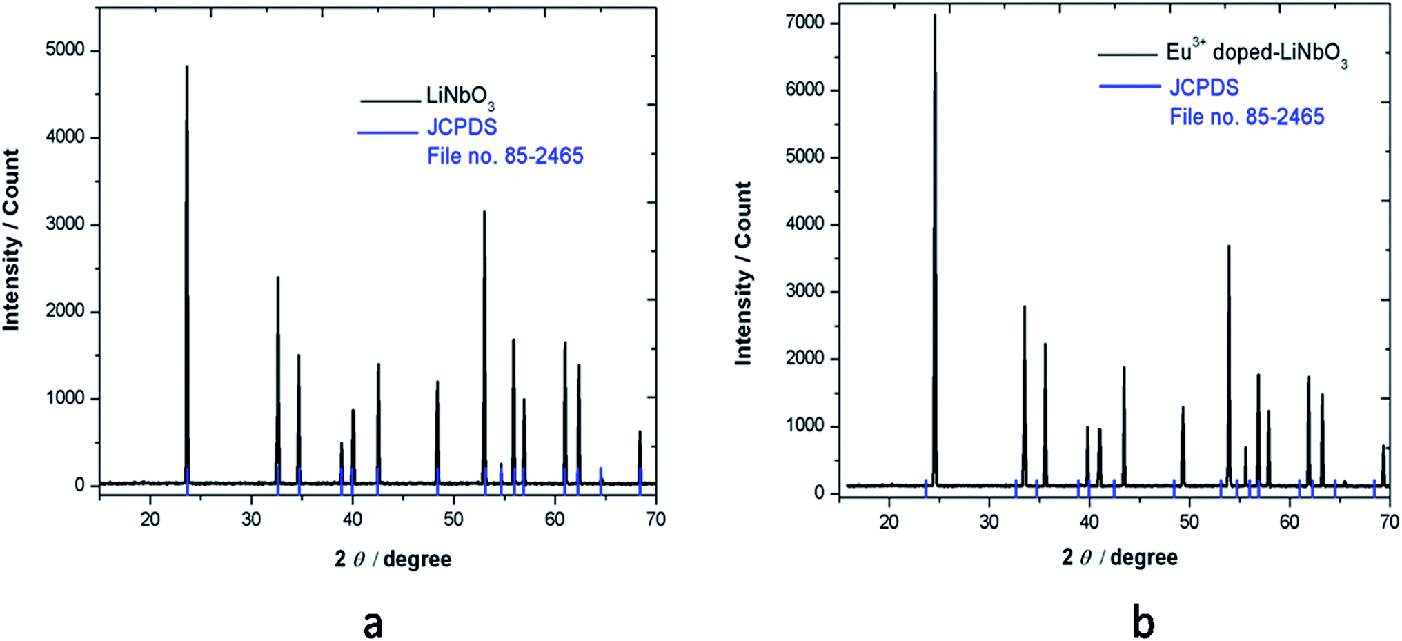 | ||
| Fig. 1 XRD pattern of (a) LiNbO3 and (b) Eu3+ doped LiNbO3. | ||
3.2. Fourier-transform infrared (FTIR) spectroscopy study of LNO and Eu3+ doped LNO
The FTIR spectra were recorded using a diamond single reflection ATR probe Alpha Bruker-500 spectrometer. For LNO and Eu3+ doped LNO, the FTIR spectra have been shown in Fig. 2, and it shows that for both niobates, the absorption peaks exist in the range of 500–1000 cm−1, which can be attributed the NbO6 octahedron.31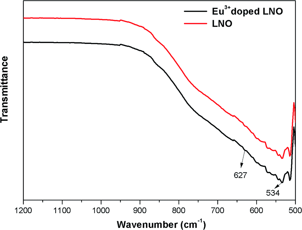 | ||
| Fig. 2 FTIR spectra of LNO and Eu3+ doped LNO. | ||
3.3. Photoluminescence study
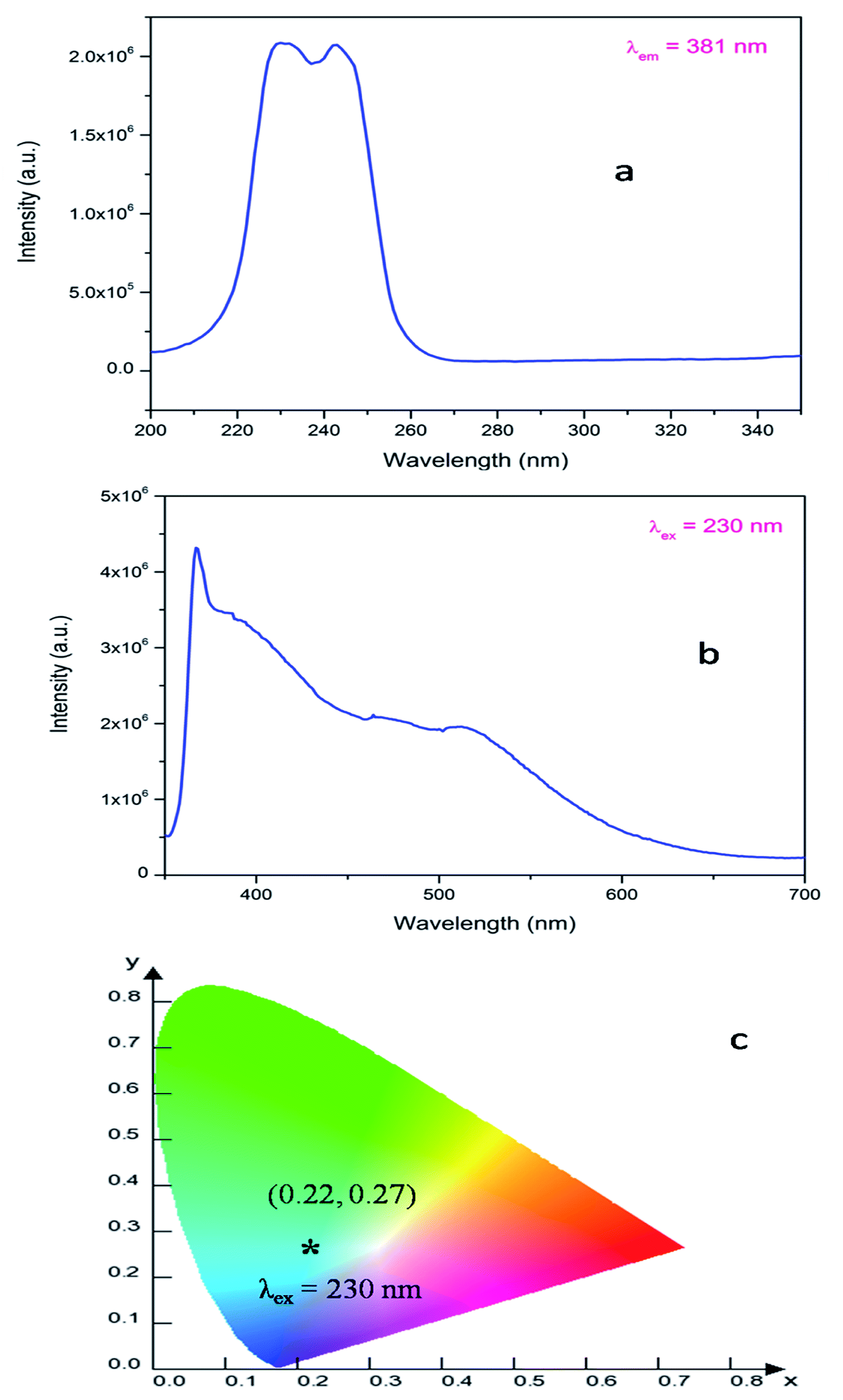 | ||
| Fig. 3 Photoluminescence (a) excitation and (b) emission spectra of LNO recorded at room temperature and (c) the corresponding CIE color co-ordinates. | ||
In order to identify various defect centres responsible for the host emission, PL lifetime measurements were carried out at 230 nm excitation and at different host emission band such as at 380 nm, 440 nm and 540 nm and the decay curves are presented by Fig. S1 provided in the ESI.† Similar to our earlier cases of several defect related luminescence material,32 in LNO compound also, there is a possibility of getting multiple lifetime value at single emission wavelength due to overlap by other emission bands. However, we have considered only that lifetime value which has maximum contribution among all. The respective lifetime values are 113.16 μs for 380 nm color components, 618.40 μs for 440 nm color component and 130.83 μs for 540 nm color component. Further to confirm their existence in the broad emission spectra, we have carried out the Time Resolved Emission Spectra (TRES) analysis at different delay time. Fig. 4 represents the TRES spectra at different delay time. It is generally assumed that the excited species are completely decayed at a time which is equal or greater than three times of their respective lifetime value (3τ). Since most of the components have lifetime value more than 100 μs, the TRES spectra at 5 μs delay time is composed of all the color components. However, as we kept on increasing the delay time, there is a gradual change in intensity of the color components. The spectra at 380 nm and 540 nm region starts disappearing, since they are the short lived species and at a delay time of 1 ms, these two components are almost disappeared from the spectra, which is now composed by the 440 nm and 500 nm components. The 500 nm component was not visible in the emission spectra, however the TRES study showed that there is a color emitting component at 500 nm region which is having higher lifetime value than the 440 nm component that is 1908.30 μs.
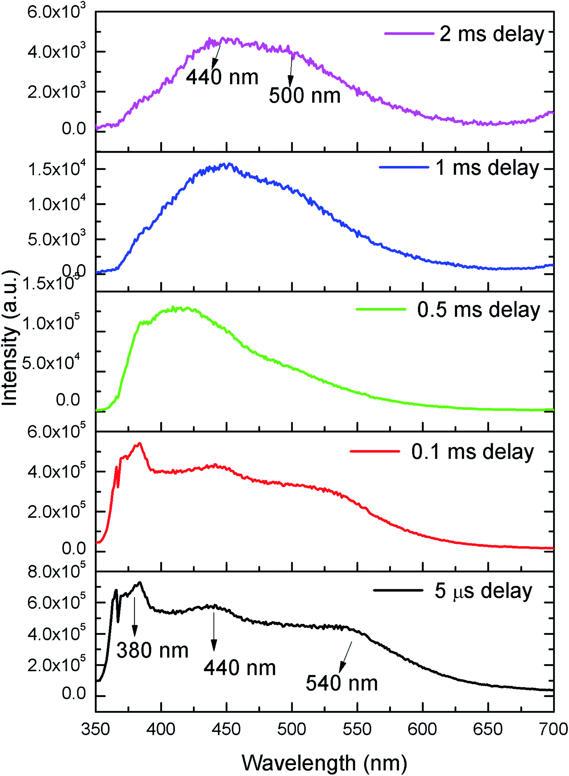 | ||
| Fig. 4 TRES spectra of LNO at different delay time. | ||
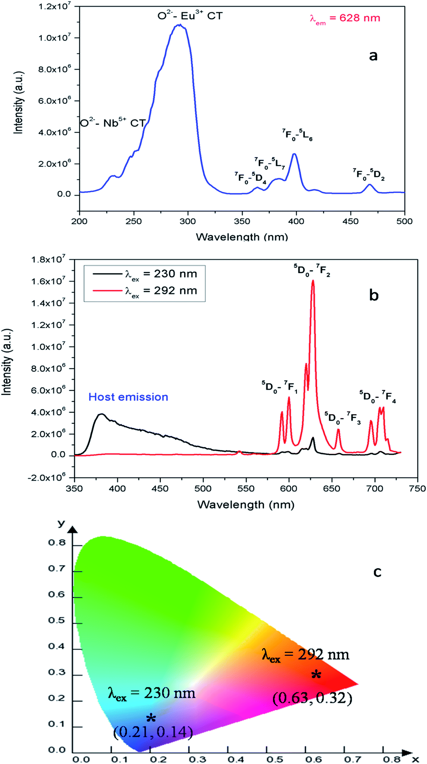 | ||
| Fig. 5 (a) Photoluminescence excitation and (b) emission spectra of Eu:LNO recorded at room temperature and (c) the corresponding CIE color co-ordinates. | ||
Fig. 5b represents the emission spectrum of Eu:LNO+ upon excitation with both the host absorption band (λmax = 230 nm) and with the CT band of Eu3+ (λmax = 292 nm). It can be seen from the respective figures that upon excitation with 230 nm the host emission band is the most intense one. On the other hand upon excitation at 292 nm the emission spectrum exhibits intense characteristics features of Eu3+ ion involving transition from 5D0 to 7FJ, J = 0–4. In this case, the host emission bands are almost disappeared. The color coordinates, as represented by the asterisk “*”, are given in the CIE chromaticity diagram in Fig. 5c, which shows that upon changing the excitation from 230 nm to 292 nm, the Eu:LNO compound changes its emission from bluish to red. This is a very interesting observation due to fact that the same compound can be used both as blue light emitting as well as red light emitting phosphor material by choosing different excitation source i.e. either with a short-wave UV source or by a long wave UV source. This can be explained on the basis of the respective CT excitation bands of host (O2− → Nb5+) and Eu3+ ion (O2− → Eu3+). When we are exciting with the 230 nm, which is CT from O2− → Nb5+, the compound is showing intense bluish host emission but at 292 nm excitation, which is due to CT from O2− → Eu3+, the compound will definitely show the red emission of Eu3+ ion. From the emission spectra of Eu3+ ions, it can also be seen that 5D0 → 7F2 electrical dipole transition (ED) around 628 nm is more intense than the 5D0 → 7F1 magnetic dipole (MD) transition around 595 nm. This indicates that most of the Eu3+ ions in LNO are occupying an asymmetric site.31,33 Let us propose a possible band structure model by Fig. 6, which pictorially explains all these observation. All these electronic states are later explained in out DFT calculation part. From Fig. 6a, it can be seen that the electrons are being excited from filed p orbital of O to vacant d orbital of Nb5+ at 230 nm wavelength. Now since this state is very close to many defect related energy states or the conduction band, the electrons can transfer to these states via the conduction band and thereby gives rise to various defect related emissions. In Fig. 6b, the electrons from p orbital of O to vacant d orbital of Eu3+ ion are excited at 292 nm wavelength and gives rise to its characteristics emissions. A detail study of these energy states are given latter in the theoretical part.
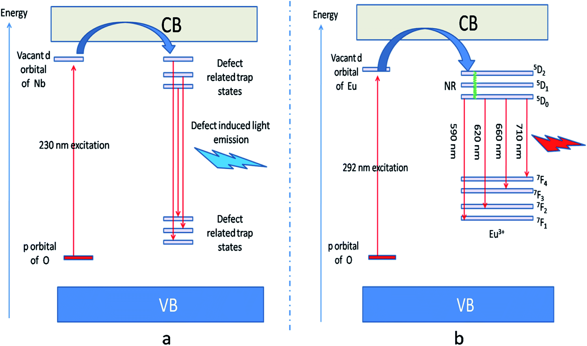 | ||
| Fig. 6 (a) defect induced host emission at 230 nm excitations and (b) Eu3+ ions emission at 292 nm excitation. The defect related trap states are observed from DFT calculation and they are due to various oxygen, Li and Nb vacancies. A pictorial summary of such defect related energy states inside the band gap has been given in Fig. S2 in ESI.† | ||
In order to understand the local environment and site occupancy of Eu3+ ions in LNO, PL lifetime experiments were carried out at 395 nm excitation and 628 nm emission wavelengths. The decay curve was best fitted with the bi-exponential eqn (1) as shown in Fig. 7.
 | (1) |
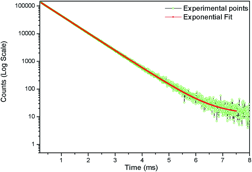 | ||
| Fig. 7 Photoluminescence decay curve of LNO:Eu3+ at λex = 395 nm with (a) λem = 628 nm. | ||
To calculate the percentage of a specific lifetime component the following formula can be used
 | (2) |
The two different lifetimes obtained from the decay curve are τ1 = 643.16 μs and τ2 = 706.99 μs with the relative percentage of 23% and 77% respectively. The average lifetimes (τave) is calculated using the eqn (3).
 | (3) |
The observation of two lifetime values suggests that Eu3+ ions must be placed in two different lattice environments. From ionic radii consideration, 6 co-ordinates Eu3+ is larger (ionic radii = 0.94 Å) in size compared to both 6 co-ordinate Nb5+ (ionic radii = 0.64 Å) and 6 co-ordinate Li1+ (ionic radii = 0.76 Å). If Eu3+ ions go to any of these two lattice sites then there will a charge difference of 2, either negative or positive and to compensate this charge imbalance there will be creation either positively charged oxygen vacancies (formation of a VO2+, if Eu3+ ion goes to Nb5+ site) or negative charged cationic vacancies (formation of 2VLi1−, if Eu3+ ion goes Li1+ site). From our theoretical calculation we have observed that formation energy of VO2+ is less compared to that of VLi1−. Further there should be creation of two Li-vacancies if Eu3+ goes to Li+ site. Thus Eu3+ ion has more preference to go to the Nb5+ site. Therefore, the τ2 = 706.99 μs component with a relative percentage of 77% might be due to Eu3+ ions at Nb5+ site while τ1 = 643.16 μs with a relative percentage of 23% might be due to Eu3+ ions at Li+ site. We have also observed from theoretical calculation that a Eu3+ ion replacing Nb5+ site is energetically more favorable.
In present case the 5D0 → 7F0 transition is absent and hence the site symmetry should not be among those mentioned above.
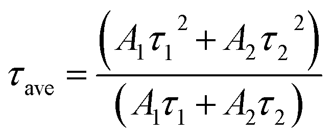
In case of Eu:LNO, the substitutions of Li3+ with Eu3+ will not result significant lattice distortion because of size difference is less. From stark splitting pattern shown in Fig. 8, two peaks for 5D0 → 7F1 MD transition, three peaks for 5D0 → 7F2 ED transition and four peaks for 5D0 → 7F4 transition of Eu3+ ion were resolved for Eu:LNO. Therefore from the branching rules for various point groups;37,38 we can say that in Eu:LNO the actual site symmetry of Eu3+ is D3. Thus it can be conclude that upon Eu3+ doping the structure becomes less symmetric due to distortion.
 | ||
| Fig. 8 Stark splitting pattern of the characteristics emission lines of Eu3+ ion in LNO. | ||
3.4. Electrical properties
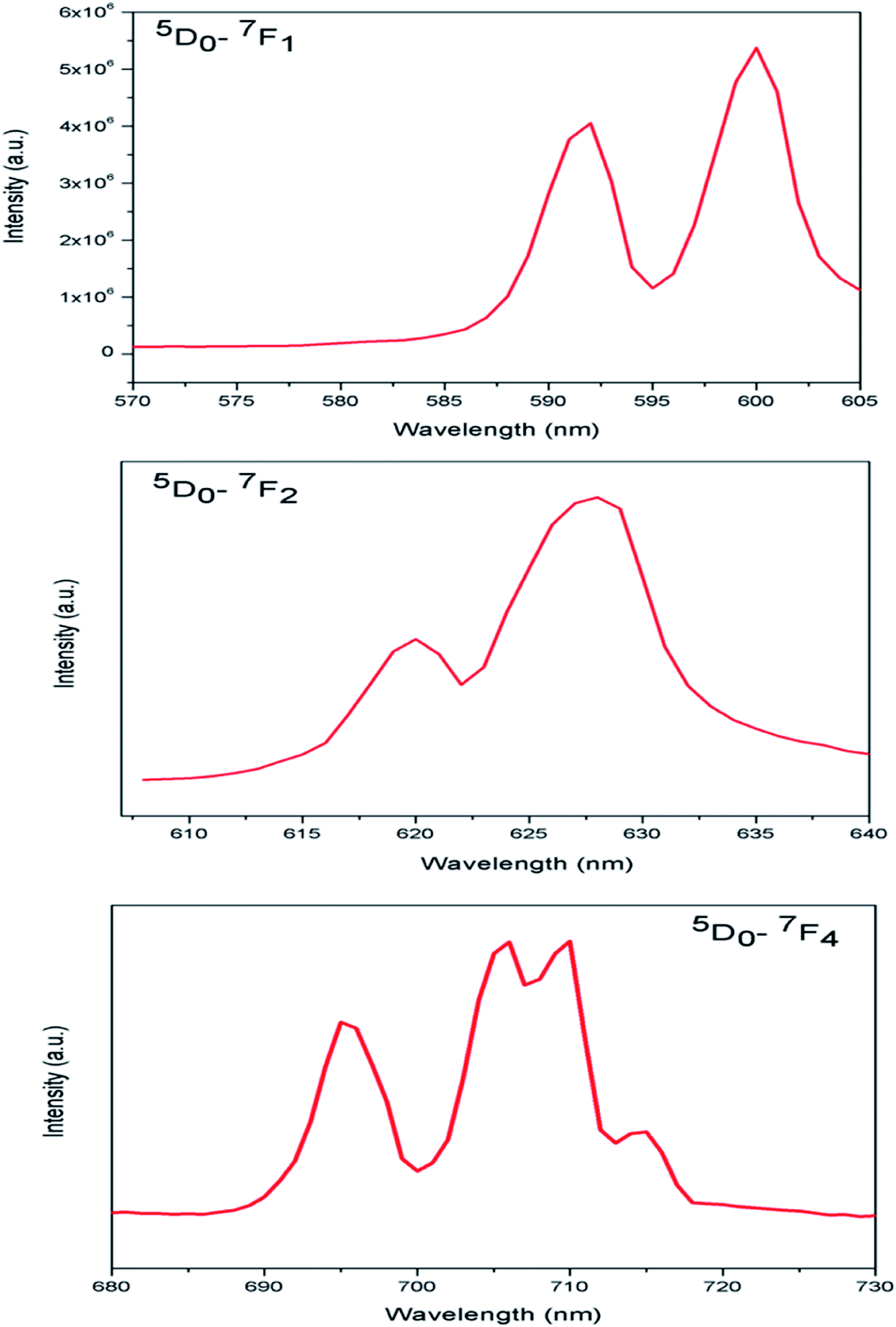
The ferroelectric (P–E) hysteresis loops of the Eu:LNO at room temperature and at different electrical field is shown in Fig. 9. It is observed that the polarisation is maximum at 5 kV cm−1. It is very crucial to characterize the ferroelectric behaviour from P–E loop and earlier reports showed that the compounds which shows saturation in polarization and have concave region in P–E plot are true ferroelectric in nature.39 The present compound also showed saturation polarization and concave region, which indicates the presence of intrinsic ferroelectricity. | ||
| Fig. 9 Ferroelectric (P–E) hysteresis loops of the Eu:LNO at room temperature at different electrical field. | ||
Fig. 10 represents the ferroelectric (P–E) hysteresis loops for undoped and Eu3+ doped samples at a field 5 kV cm−1. The respective remnant polarization of Eu:LNO and LNO samples are Pr = 3.3652 μC cm−2 and Pr = 0.30 μC cm−2 respectively. While the energy loss are 13![[thin space (1/6-em)]](https://www.rsc.org/images/entities/char_2009.gif) 864.5 μJ cm−2 for Eu:LNO and 1311.82 μJ cm−2 for LNO. Figure represent the leakage current density vs. field plot for Eu:LNO and LNO, from which it can be seen that the leakage current is more at any point of field for Eu:LNO compare to LNO.
864.5 μJ cm−2 for Eu:LNO and 1311.82 μJ cm−2 for LNO. Figure represent the leakage current density vs. field plot for Eu:LNO and LNO, from which it can be seen that the leakage current is more at any point of field for Eu:LNO compare to LNO.
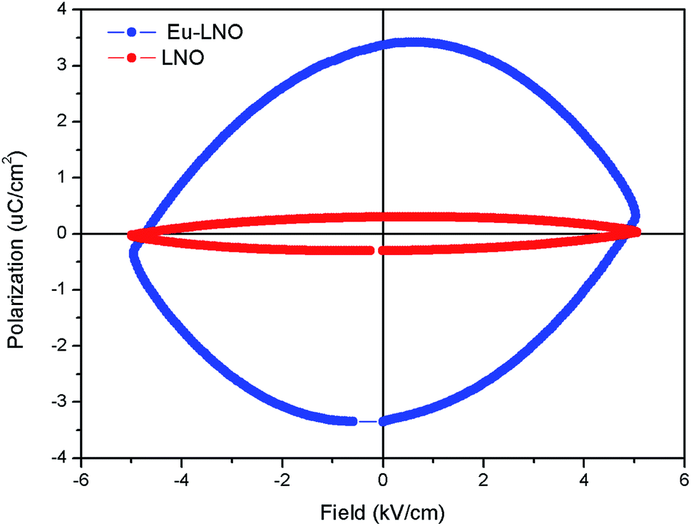 | ||
| Fig. 10 Ferroelectric (P–E) hysteresis loops for undoped (LNO) and Eu3+ doped samples (Eu–LNO) at a field 5 kV cm−1. | ||
A detail description of crystal structure of LNO shows that it belongs to a R3c space group.40,41 The oxide ions are arranged in nearly hexagonal close-packed planar sheets and the stacking sequence of cations in these octahedral sites is: Nb, Li, vacancy, Nb, Li, vacancy… and so on or LiO6, NbO6 and VO6…, where V stands for vacancy. It is worth to note here that one third of the octahedral interstices are filled by lithium atoms, another one-third filled by niobium atoms, and the remaining one-third is vacant. The Li and Nb ions are placed significantly off-center from the centrosymmetric positions along the polar axis and this result in spontaneous polarization. Therefore, any distortion at Li or Nb-site in the matrix will affect the position of these ions and change the spontaneous polarization. Thus, the increase in polarization of LNO matrix upon doping with Eu3+ ion can be correlated with relatively more off-center position of these Nb and Li ions due to substitution of Eu3+ ion. It is quite obvious that 6-coordinated Eu3+ ion has bigger ionic radii than same coordinated Nb5+ and Li+ ion. Therefore, there will be high degree of distortion in the matrix due to substitution of smaller ion by bigger ion. Further, the charge imbalance will cause addition distortion and may results in several defect centers. This is also reflected in the leakage current density plot in Fig. 11 which showed that the leakage current is more when Eu3+ is doped into the LNO matrix. As stated earlier that Eu3+ substitution at Nb-site of LNO results in defects, which may increase the ionic conductivity. This increased conductivity causes more leakage in current. The enhancement of polarization also indicates that the dopant ion Eu3+ is going to the lattice site and not to the vacant interstices site, otherwise a decrease in polarization would have been observed since it would restrict the displacement of Li or Nb to other side of oxygen triangle.
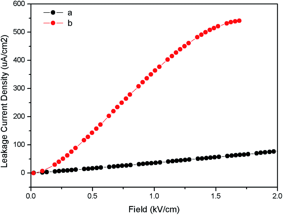 | ||
| Fig. 11 Leakage current density vs. field (a) LNO and (b) Eu:LNO. | ||
3.5. Electronic structure and band gap energy of LNO and the possible explanation for photoluminescence and electrical observations
The DFT calculation mythologies are given in the ESI.† Generally, at room temperature the ground state of LNO is ferroelectric with space group R3c while at high temperature (≥1480 K), the stable phase is high-symmetric paraelectric phase with space group R![[3 with combining macron]](https://www.rsc.org/images/entities/char_0033_0304.gif) c. In ferroelectric (R3c) phase, the Li and Nb atoms are located at 6a Wyckoff position (in hexagonal axes) with internal parameter zNb, and O atoms are located at 18b Wyckoff position with parameters u, v, and w. We have followed the notation of ref. 42, the DFT-GGA calculated unit cell parameters are: a = 5.197 Å, c = 14.017 Å, zNb = 0.0329, u = 0.00881, v = 0.0388, and w = 0.0191. The reported unit cell parameters by experiment43 are a = 5.151 Å, c = 13.876 Å, zNb = 0.0329, u = 0.00947, v = 0.0383, and w = 0.0192 and the deviation is less than 3% for the ferroelectric phase. Our GGA-PBE calculated results (given in Table 1) are also in well agreement with the GGA-PW91 results reported by Veithen and Ghosez.44
c. In ferroelectric (R3c) phase, the Li and Nb atoms are located at 6a Wyckoff position (in hexagonal axes) with internal parameter zNb, and O atoms are located at 18b Wyckoff position with parameters u, v, and w. We have followed the notation of ref. 42, the DFT-GGA calculated unit cell parameters are: a = 5.197 Å, c = 14.017 Å, zNb = 0.0329, u = 0.00881, v = 0.0388, and w = 0.0191. The reported unit cell parameters by experiment43 are a = 5.151 Å, c = 13.876 Å, zNb = 0.0329, u = 0.00947, v = 0.0383, and w = 0.0192 and the deviation is less than 3% for the ferroelectric phase. Our GGA-PBE calculated results (given in Table 1) are also in well agreement with the GGA-PW91 results reported by Veithen and Ghosez.44
| a | c | z | u | v | w | |
|---|---|---|---|---|---|---|
| a For LiNbO3, in hexagonal coordinate, z, u, v and w were defined (0; 0; 1/4 + z) for Li1, (0, 0, 0) for Nb1, and (−1/3 − u; −1/3 + v; 7/12 − w) for O1 (ref. 45). | ||||||
| DFT-GGA (this study) | 5.197 | 14.017 | 0.0329 | 0.00881 | 0.0388 | 0.0191 |
| Experiment43 | 5.151 | 13.876 | 0.0329 | 0.00947 | 0.0383 | 0.0192 |
| DFT-LDA42 | 5.086 | 13.723 | 0.0350 | 0.01497 | 0.0247 | 0.0186 |
| DFT-GGA44 | 5.067 | 13.721 | 0.0337 | 0.01250 | 0.0302 | 0.0183 |
| DFT-GGA45 | 5.161 | 13.901 | 0.0339 | 0.01205 | 0.0278 | 0.0191 |
The density of states (DOSs) of ideal ferroelectric phase of LNO is plotted in Fig. 12(a). The band between −18 eV and −15 eV is mainly contributed by O 2p state. The upper valence-band (VB) lying in the range 0 and −5 eV can be divided into two different regions. In the low-energy region it can be observed that the O 2p states are strongly hybridize with Nb 4d states while the high-energy region was found to be predominately contributed by the O 2p states. The conduction band (CB) above the Fermi level of LNO is found to be dominated by Li 2s/2p states and O 2p states. This suggests that there is a possibility of charge transfer transition from 2p orbital of oxygen to 4d orbital of Nb as observed in our photoluminescence excitation spectra of LNO represented by Fig. 3a. The electronic band-gap in ferroelectric phase is 3.24 eV, which is in well agreement with reported result of 3.48 eV calculated by DFT-GGA.45
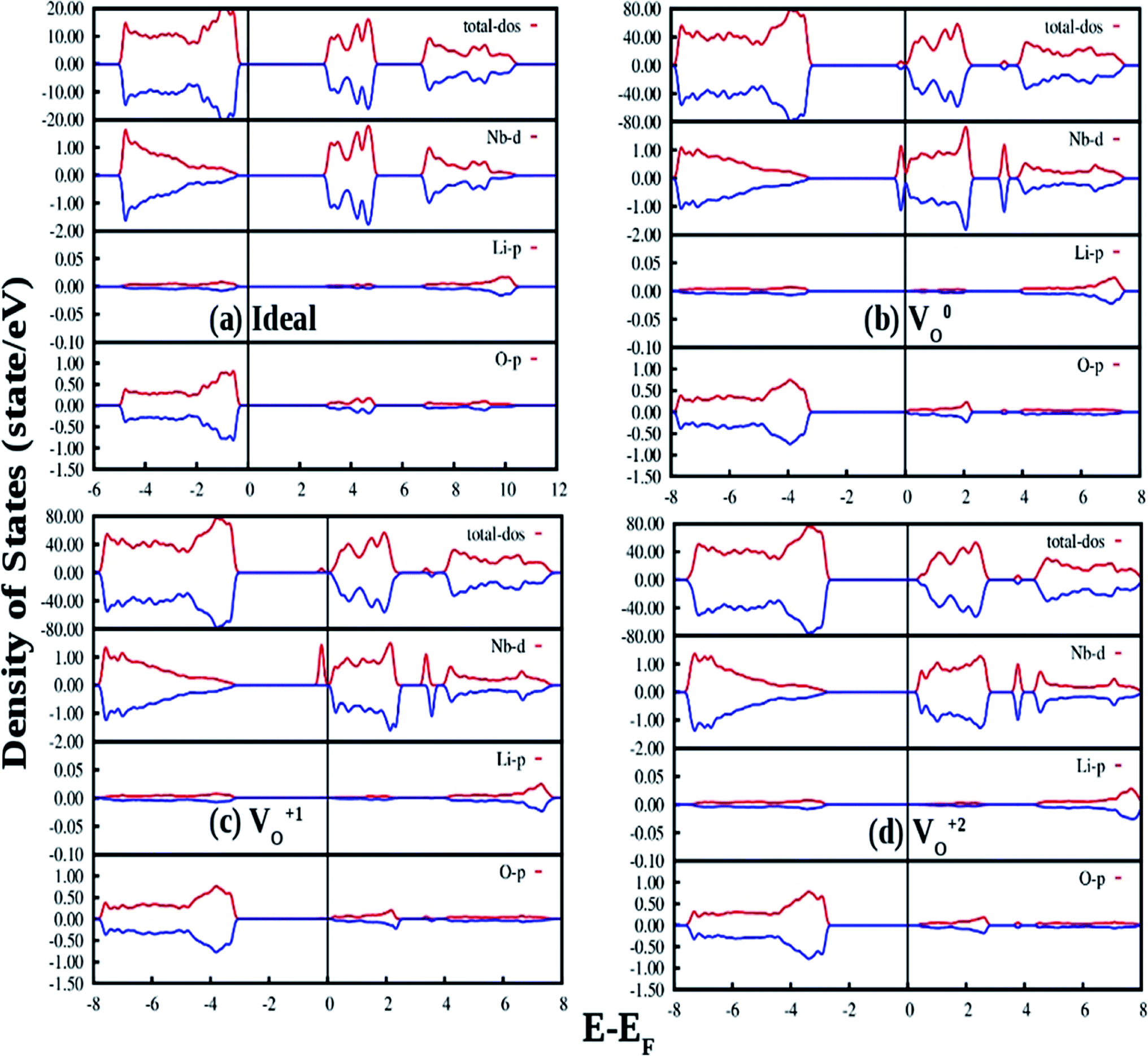 | ||
| Fig. 12 Total and species projected DOS for (a) ideal LNO and with (b) neutral oxygen vacancy (V0O or F0), (c) singly charges oxygen vacancy (VO1+, F+) and (d) doubly charged oxygen vacancy (VO2+, F2+) calculated in a 120 atom supercell using DFT-GGA. The Fermi energies are represented by vertical lines at zero energy. The DOS for spin-up and spin-down states are represented by red and blue color respectively. | ||
Fig. 12(b) shows our GGA-PBE calculated DOS of LNO with a single neutral oxygen vacancy (V0O). Overall DOS features are similar to the ideal LNO case but an impurity states appear just below the CB minimum. The impurity states contribute both in majority and minority spin-component. It can be seen that the impurity state is mainly contributed by the Nb d state, which results in reduction of the electronic band-gap to 2.8 eV. Fig. 12(c) represents the GGA-PBE calculated DOS of LNO with a single +1 charge oxygen vacancy (VO1+). Overall DOS features are similar to the ideal LNO case but an impurity states appear just below the CB minimum. This impurity state contributes only in majority spin-component and contributed by the Nb d states. As a result the electronic band-gap is reduced to 2.7 eV. Fig. 12(d) represents the GGA-PBE calculated DOS of LNO with a single +2 charge oxygen vacancy (VO2+). Overall DOS features are similar to the ideal LNO case and no impurity states appear in the electronic band-gap region. The electronic band-gap was calculated to be 3.0 eV. In ideal LNO case Fermi energy is situated just above the VB maxima and in oxygen defect case (V0O, VO1+, VO2+) it is situated just below the CB minima. Therefore these impurity states inside the band gap in cases of VO1+ and V0O may be responsible for many electronic transition and gives rise to multicolor emission presented in Fig. 3a and 4. A pictorial representation of the defect related impurity electronic states is presented by Fig. S2 in the ESI.†
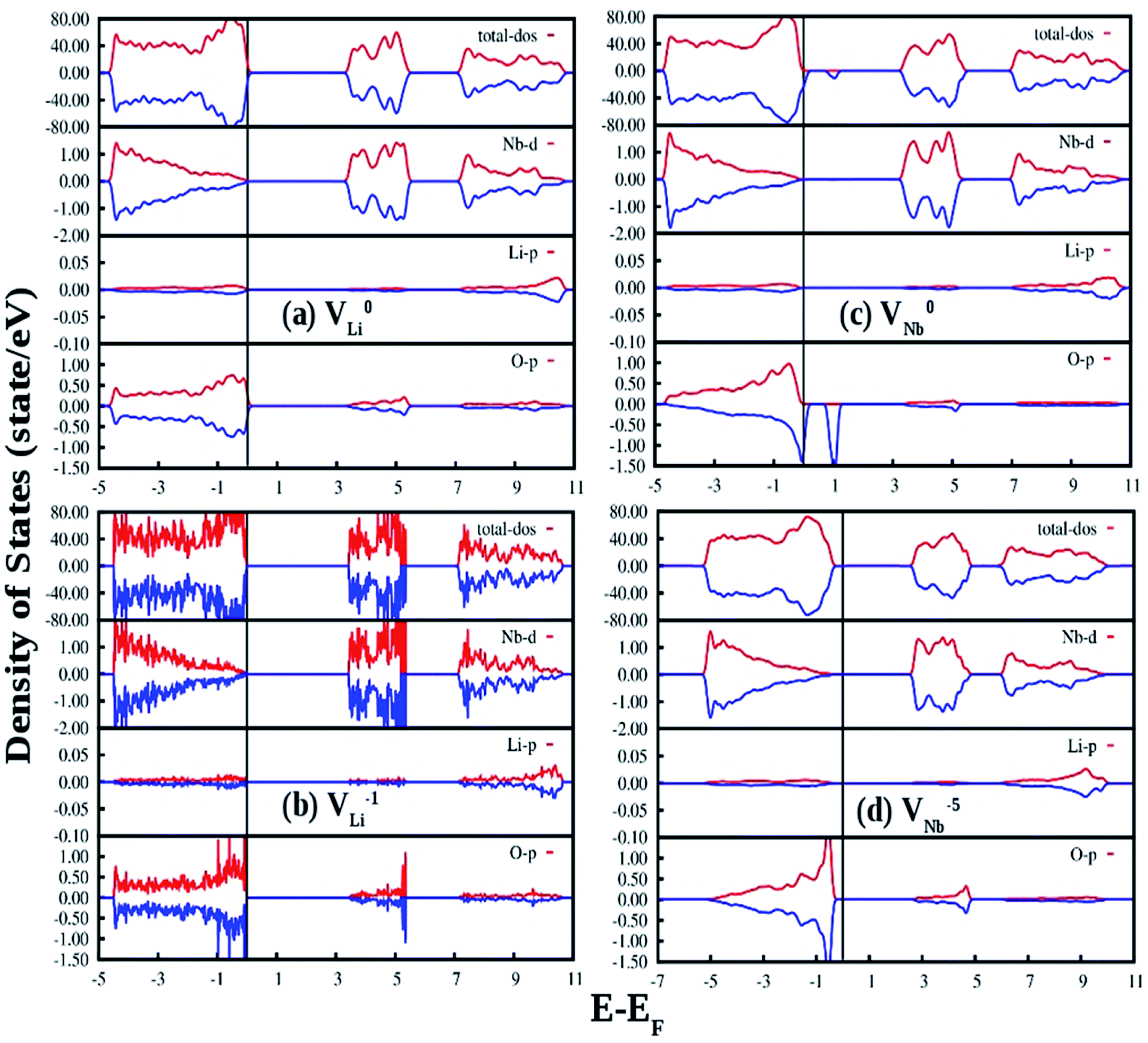
Fig. 13(a) and (b) represent the GGA-PBE calculated DOS of LNO with a single neutral and −1 charge Li vacancy (V0Li and VLi1−), respectively. Overall DOS features are similar to the ideal LNO case and a few states are extended just above the Fermi energy with no other impurity states in the electronic band-gap region. The band-gap in V0Li and VLi1− case is 3.17 and 3.30 eV, respectively, and Fermi energy is situated just above the VB maxima. Fig. 13(c) and (d) represents the GGA-PBE calculated DOS of LNO with a single neutral and −5 charge Nb vacancy (V0Nb and VNb5−), respectively. The DOS feature of V0Nb is severely distorted in minority spin component as the minority spin component of 2p states of O atom situated in the 1st nearest neighbor to the Nb atom is modified. Moreover, an impurity state appear 0.5 eV ahead of VB maxima in minority spin component. In this case the degeneracy between spin-components are lifted. The electronic band gap in V0Nb case is 3.0 eV. The DOS due to VNb5− is almost resemblance the DOS of ideal LNO and the electronic band-gap is 2.57 eV. Therefore, the Li vacancies have least effect on the DOS and Nb vacancies distort the DOS appreciably. From electronic transition point of view, only V0Nb gives rise to an additional electronic state inside the band gap and may take part in the host emission band.
 | ||
| Fig. 13 Total and species projected DOS for LNO with (a) neutral Li oxygen vacancy (V0Li), (b) −1 charge Li vacancy (VLi1−), (c) neutral Nb vacancy (V0Nb) and (d) −5 charge Nb vacancy (VNb5−) calculated in a 120 atom supercell using DFT-GGA. The Fermi energies are represented by vertical lines at zero energy. The DOS for spin-up and spin-down states are represented by red and blue color respectively. | ||
Fig. 14(a) shows our GGA-PBE calculated DOS of LNO with an antisite defect where position of one Li and Nb atom is exchanged in the 120 atom supercell. Overall DOS features are similar to the ideal LNO case and no impurity states appear in the electronic band-gap region. The Fermi energy has shifted to the bottom of the CB minima in this case. But the Nb d-states present in the CB region is modified and the electronic band-gap is 2.30 eV in this case. Thus antisite defects have no role in the host emission. Fig. 14(b) and (c) shows our GGA-PBE calculated DOS of LNO with a Eu atom doping in Li and Nb site, respectively, in the 120 atom supercell. In our calculation one Eu atom is placed in Li and Nb site by removing 1 Li and 1 Nb atom out of 24 atoms. Due to Eu doping in Li site the Fermi energy has shifted to the bottom of the CB minima. An impurity state appears just below the CB minima in the minority spin component. The impurity state is composed of Eu d-states. On the contrary, a impurity state appears just above the VB maxima in both minority and majority spin component in case of Eu doping Nb site and the impurity state is contributed by the Eu f states. The Fermi energy is situated just above the VB maxima for the Eu doping in Nb site. The electronic band-gaps are 2.25 and 2.40 eV for the Eu doping in Li and Nb site, respectively. From the DOS in cases of Eu placed at Nb site, it can be seen in the conduction band the vacant impurity states due to p orbital of oxygen and d and f orbital of Eu are closely placed around 4 eV. Thus there is probability that the excited electron from the p orbital can transfer to the vacant d or f orbitals of Eu3+ ion and gives rise to charge transfer transition. As observed in our excitation spectra of the Eu:LNO compound in Fig. 5a the excitation peak near to 292 nm might be therefore due to O2− → Eu3+ charge transfer transition. For, Eu3+ at Li-site there is no matching of the electronic states of the vacant p orbital of oxygen with that of the d and f orbital of Eu3+ ions. Therefore, the O2− → Eu3+ charge transfer transition in Fig. 5a might be attributed to Eu3+ ion occupying the Nb-site.
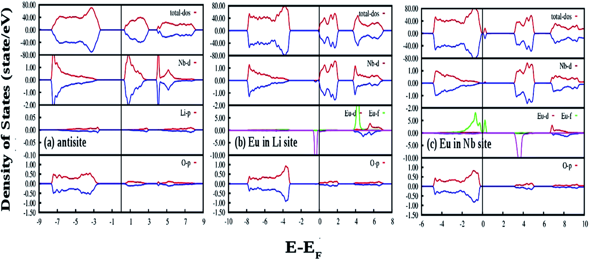 | ||
| Fig. 14 Total and species projected DOS for LNO with (a) antisite defect and (b and c) shows the DOS of LNO with Eu doping in Li and Nb site, respectively, calculated in a 120 atom supercell using DFT-GGA. The Fermi energies are represented by vertical lines at zero energy. The DOS for spin-up and spin-down states are represented by red and blue color respectively. | ||
The various defect formation energies of LNO is given by
 | (4) |
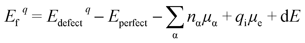
The variation of DFT calculated defect formation energies of O, Li and Nb in various charge states in the dilute limit as a function of Fermi energy is shown in Fig. 15 (left panel). From the DFT calculated formation energies for different vacancies, it can be said that in comparison to VO1+ and V0O, the formation energies VO2+ defects are low in the 0 to 2.4 eV range (in EF–EV scale) near the valence band. Thus oxygen vacancies may behave as n-type defect and to donate electrons. Similarly, we can say that VO1+ defect are favored to be formed in the 2.4 to 3.0 eV (in EF–EV scale) and beyond this range V0O defects are favored to be formed. The electronic band-gap of LiNbO3 is 3.24 eV observed from the present DFT-GGA calculation.
 | ||
| Fig. 15 DFT-GGA calculated defect formation energy (Ef) as a function of Fermi level (EF) for charged defect states (q). Three charge-state transition levels are shown and they are a deep donor level ε (+2/+1) at 2.4 eV (516 nm), a deep donor level ε (+1/0) at 3.0 eV (413 nm) and another level ε (Li1−/Nb5−) at 2.2 eV (563 nm). These charge-state transition levels with respect to the host referred binding energies (HRBE) are shown in a conventional diagram on the right hand side. | ||
Three charge-state transition levels as observed from present DFT calculation are shown in Fig. 15 (right panel) and they are a deep donor level ε (+2/+1) at 2.4 eV (516 nm), a deep donor level ε (+1/0) at 3.0 eV (413 nm) and another level ε (Li1−/Nb5−) at 2.2 eV (563 nm). Here we have defined the impurity levels as the charge-state transition levels (ε (q1/q2), from charge q1 to q2) and we have considered the Fermi level locations where different defect states with different charges have the same formation energy. These charge-state transition levels with respect to the host referred binding energies (HRBE) are shown in a conventional diagram on the right hand side of Fig. 14. We have observed similar emission bands at similar wavelength region in undoped LNO. Hence, the transition between different oxygen vacancies might be responsible for those emissions.
In order to determine energy preferences to incorporate Eu in LNO lattices at Li and Nb sites, the incorporation energies were calculated. The incorporation energy of a Eu atom at a defect site, for example Eu at an lithium vacancy site, is given by,
| E[Eu(VLi)] = E[EuLiLin−1NbnO3n] − E[Lin−1NbnO3n] − E[Eu] | (5) |
In undoped LNO, Li/Nb atoms forms LiO6/NbO6 polyhedra at distances 2.09 (3 bonds), 2.26 Å (3 bonds)/1.89 (3 bonds), 2.16 Å (3 bonds) shown as solid horizontal lines in bond-length distribution curve. In Eu:LNO (Eu in Nb site), Li–O and Nb–O bond-lengths are distributed in the range 2.02–2.13, 2.17–2.28 Å and 1.86–1.92, 2.02–2.23 Å, respectively (as shown in Fig. 16).
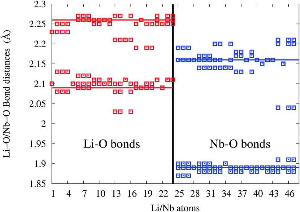 | ||
| Fig. 16 Li–O and Nb–O bond-length distribution in Eu:LNO at Nb-site. Solid red and blue lines are the Li–O and Nb–O bond-lengths in undoped LiNbO3. | ||
The x-axis of Fig. 16 shows the Li (24 atoms) and Nb (23 atoms) atoms in the 120 atoms supercell. Based on this analysis, it is evident that Eu-doping distort the LNO lattice. Similar observation can also be made from the contour plots of pure LNO and Eu:LNO. The distorted charge density contours can be identified around the Eu atoms in the (001) plane in Fig. 17. This structural distortion is responsible for the enhancement of ferroelectric properties in LNO compound.
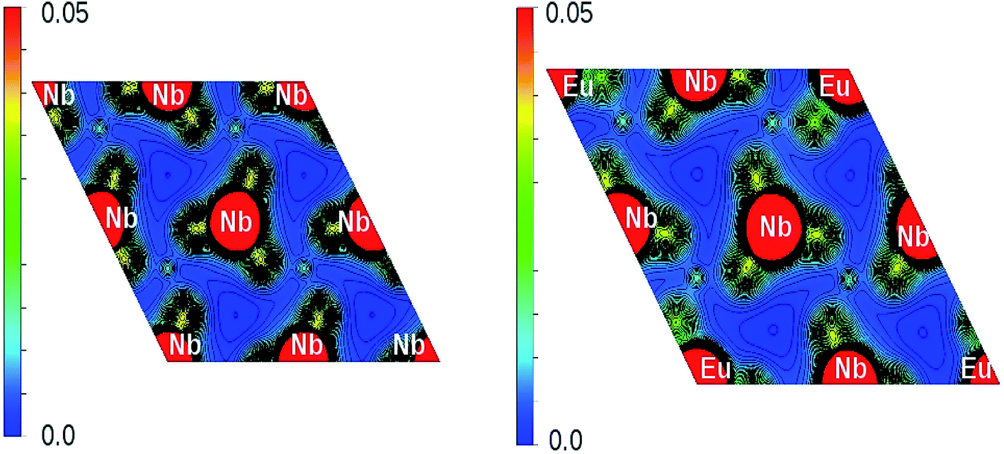 | ||
| Fig. 17 Charge density distribution (in e Å−3) plot on (001) plane of LNO (left panel) and Eu:LNO (right panel). | ||
4. Conclusion
Multifunctional LNO and Eu:LNO3 compounds are synthesised through solid state method followed by their characterisation with XRD and FTIR. Photoluminescence study reveals that the undoped compound is a blue light emitting material, while upon doping with Eu3+, the compound turned to be both as blue and red emitting phosphor materials, depending upon the excitation wavelength. The blue emission from the host is attributed to several defect canters which creates many electronic states inside the band gap. Using TRES study we have isolated the defect related emissions. Both undoped and Eu3+ doped compounds are found to show ferroelectric behaviour, however, the remnant polarization has been increased for Eu3+ doped compound with higher leakage current density. Since the ferroelectric properties in LNO are originated due to structural distortion, the enhancement of remnant polarization was due to more distortion induced by the Eu3+ dopant ion, which has larger ionic radii than host cations and different charge. The fact that the structure became more distorted was also supported by the fact that the point symmetry calculated from stark-splitting pattern of the characteristics emission of Eu3+ ions was found to be changed from the reported C6v for undoped to D3 when Eu3+ ions are doped. From DFT based theoretical calculation, various electronic states originated from different defect centers are found to exist inside the band gap of the material, which results in the multicolor host emission. The charge transfer transition has also been explained by DFT calculation. It was also observed that Eu3+ ions energetically favor to occupy the Nb site. Further from DFT calculation it was observed that there is a change in the structural parameters due to structural distortion when Eu3+ is doped, which justified the fact that the structural distortion lead to tuning of the electrical properties.Conflicts of interest
All authors are hereby declared that there is no conflict of interest.Acknowledgements
The authors thank Dr Bal Govind Vats FCD, BARC for the FTIR measurements. The work is fully funded by our own institute i.e. BARC. No external funding agency was involved.References
- L. T. Canham, Appl. Phys. Lett., 1990, 57, 1046–1048 CrossRef CAS.
- H. Ohno, Science, 1998, 281, 951–956 CrossRef CAS PubMed.
- X. S. Wang, C. N. Xu, H. Yamada, K. Nishikubo and X. G. Zheng, Adv. Mater., 2005, 17, 1254 CrossRef CAS.
- H. Zou, D. F. Peng, G. H. Wu, X. S. Wang, D. H. Bao, J. Li, Y. X. Li and X. Yao, J. Appl. Phys., 2013, 114, 073103 CrossRef.
- H. Q. Sun, D. F. Peng, X. S. Wang, M. M. Tang, Q. W. Zhang and X. Yao, J. Appl. Phys., 2011, 110, 016102 CrossRef.
- X. Wang, D. Peng, B. Huang, C. Pan and Z. L. Wang, Nano Energy, 2019, 55, 389–400 CrossRef CAS.
- G. F. Teixeira, E. S. Junior and A. Z. Simões, CrystEngComm, 2017, 19, 4378 RSC.
- (a) H. Wei, H. Wang, Y. Xia, D. Cui, Y. Shi, M. Dong, C. Liu, T. Ding, J. Zhang, Y. Ma, N. Wang, Z. Wang, Y. Sun, R. Wei and Z. Guo, J. Mater. Chem. C, 2018, 6, 12446–12467 RSC; (b) Y. Zhang, X. Pan and Z. Wang, RSC Adv., 2015, 5, 20453 RSC.
- J. H. Jung, M. Lee and J. I. Hong, ACS Nano, 2011, 5, 10041 CrossRef CAS PubMed.
- S. M. Neumayer, A. V. Ievlev, L. Collins, R. Vasudevan, M. A. Baghban, O. Ovchinnikova, S. Jesse, K. Gallo, B. J. Rodriguez and S. V. Kalinin, ACS Appl. Mater. Interfaces, 2018, 10(34), 29153–29160 CrossRef CAS PubMed.
- M. Friedrich, W. G. Schmidt, A. Schindlmayr and S. Sanna, Phys. Rev. Mater., 2017, 1, 034401 CrossRef.
- O. F. Schirmjzr, O. Thiemann and M. W. Hlecke, J. Phys. Chem. Solids, 1991, 52, 185–200 CrossRef.
- H. Megaw and C. N. W. Darlington, Acta Crystallogr., Sect. A: Cryst. Phys., Diffr., Theor. Gen. Crystallogr., 1975, 31, 161 CrossRef.
- H. J. Xiang, Phys. Rev. B: Condens. Matter Mater. Phys., 2014, 90, 094108 CrossRef.
- K. E. Johnston, C. C. Tang, J. E. Parker, K. S. Knight, P. Lightfoot and S. E. Ashbrook, J. Am. Chem. Soc., 2010, 132(25), 8732 CrossRef CAS PubMed.
- B. C. Grabmaier, W. Wersing and W. Koestler, J. Cryst. Growth, 1991, 110, 339–347 CrossRef CAS.
- C. Wang, J. Sun, W. Ni, B. Yue, F. Hong, H. Liu and Z. Cheng, J. Am. Ceram. Soc., 2019, 102, 6705–6712 CrossRef CAS.
- T. Volk, L. Ivleva, P. Lykov, N. Polozkov, V. Salobutin, R. Pankrath and M. Wöhlecke, Opt. Mater., 2001, 18(1), 179–182 CrossRef CAS.
- A. Brenier, Opt. Commun., 1996, 129, 57 CrossRef CAS.
- G. Foulon, M. Ferriol, A. Brenier, M. T. Cohen-Adad and G. Boulon, Chem. Phys. Lett., 1995, 245, 555 CrossRef CAS.
- E. Montoya, J. Capmany, L. E. Bausá, T. Kellner, A. Diening and G. Huber, Appl. Phys. Lett., 1999, 74, 3113 CrossRef CAS.
- I. Dohnke, B. Trusch, D. Klimm and J. Hulliger, J. Phys. Chem. Solids, 2004, 65, 1297 CrossRef CAS.
- K. Sanyal, N. Pathak, A. K. Yadav, B. Kanrar, R. M. Kadam, S. N. Jha, D. Bhattacharya and N. L. Misra, Dalton Trans., 2016, 45, 7650–7664 RSC.
- S. K. Gupta, N. Pathak and R. M. Kadam, J. Lumin., 2016, 169, 106–114 CrossRef CAS.
- S. K. Gupta, P. S. Ghoshb, N. Pathak and R. M. Kadam, RSC Adv., 2016, 6, 42923–42932 RSC.
- S. K. Gupta, P. S. Ghosh, C. Reghukumar, N. Pathak and R. M. Kadam, RSC Adv., 2016, 6, 44908–44920 RSC.
- J. E. Muñoz Santiuste, B. Macalik and J. García Solé, Phys. Rev. B: Condens. Matter Mater. Phys., 1993, 47, 88 CrossRef PubMed.
- D. Hreniaka, A. Speghini, M. Bettinelli and W. Streka, J. Lumin., 2006, 119–120, 219–223 CrossRef.
- D. Hreniak and W. Strek, Appl. Phys. Lett., 2006, 88, 161118 CrossRef.
- (a) N. Pathak, S. K. Gupta, P. S. Ghosh, A. Arya and V. Natarajan, RSC Adv., 2015, 5(23), 17501–17513 RSC; (b) S. K. Gupta, N. Pathak, P. S. Ghosh, B. Rajeshwari, V. Natarajan and R. M. Kadam, J. Magn. Magn. Mater., 2015, 391, 101–107 CrossRef CAS; (c) S. K. Gupta, N. Pathak, P. S. Ghosh and R. M. Kadam, J. Alloys Compd., 2017, 695, 337–343 CrossRef CAS.
- (a) R. Phatak, N. Pathak, S. Muhammed, S. K. Sali and A. Das, ChemPlusChem, 2018, 83, 1144–1152 CrossRef CAS PubMed; (b) R. Phatak, N. Pathak, S. Muhammed, A. Das and S. K. Sali, J. Am. Ceram. Soc., 2020, 103, 2617–2629 CrossRef CAS.
- (a) N. Pathak, P. S. Ghosh, S. Saxena, D. Dutta, A. K. Yadav and D. Bhattacharyya, Inorg. Chem., 2018, 57(7), 3963–3982 CrossRef CAS PubMed; (b) N. Pathak, P. S. Ghosh, S. K. Gupta, S. Mukherjee, R. M. Kadam and A. Arya, J. Phys. Chem. C, 2016, 120(7), 4016–4031 CrossRef CAS; (c) N. Pathak, P. S. Ghosh, S. K. Gupta, R. M. Kadam and A. Arya, RSC Adv., 2016, 6, 96398–96415 RSC.
- (a) N. Pathak, S. Mukherjee, D. Das, D. Dutta, S. Dash and R. M. Kadam, J. Mater. Chem. C, 2020, 8, 7149–7161 RSC; (b) D. Hebbar, K. S. Choudhari, N. Pathak, S. A. Shivashankar and S. D. Kulkarni, J. Alloys Compd., 2018, 768, 676–685 CrossRef; (c) P. Das, N. Pathak, B. Sanyal, S. Dash and R. M. Kadam, J. Alloys Compd., 2019, 810, 1519062 CrossRef.
- R. S. Weis and T. K. Gaylord, Appl. Phys. A: Solids Surf., 1985, 37, 191–203 CrossRef.
- X. Y. Chen, W. Zhao, R. E. Cook and G. K. Liu, Phys. Rev. B: Condens. Matter Mater. Phys., 2004, 70(20), 2051221–2051229 Search PubMed.
- X. Y. Chen and G. K. Liu, J. Solid State Chem., 2005, 178(2), 419–428 CrossRef CAS.
- S. V. Eliseevaa and J. C. G. Bunzli, Chem. Soc. Rev., 2010, 39, 189 RSC.
- Q. Ju, Y. Liu, R. Li, L. Liu, W. Luo and X. Chen, J. Phys. Chem. C, 2009, 113, 2309 CrossRef CAS.
- L. Hao, Y. Li, J. Zhu, Z. Wu, F. Long, X. Liu and W. Zhang, J. Alloys Compd., 2014, 590, 205–209 CrossRef CAS.
- M. Sumets, Lithium Niobate-Based Heterostructures, IOP Publishing, 2018, DOI:10.1088/978-0-7503-1729-0ch1.
- M. P. Sumets, V. A. Dybov and V. M. Levlev, Inorg. Mater., 2017, 53, 1361 CrossRef CAS.
- K. Parlinski, Z. Q. Li and Y. Kawazoe, Phys. Rev. B: Condens. Matter Mater. Phys., 2000, 61, 272 CrossRef CAS.
- H. Boysen and F. Altorfer, Acta Crystallogr., Sect. B: Struct. Sci., 1994, 50, 405 CrossRef.
- M. Veithen and P. Ghosez, Phys. Rev. B: Condens. Matter Mater. Phys., 2002, 65, 214302 CrossRef.
- W. G. Schmidt, M. Albrecht, S. Wippermann, S. Blankenburg, E. Rauls, F. Fuchs, C. Rödl, J. Furthmüller and A. Hermann, Phys. Rev. B: Condens. Matter Mater. Phys., 2008, 77, 035106 CrossRef.
- M. Leslie and M. J. Gillan, J. Phys. C: Solid State Phys., 1985, 18, 973–982 CrossRef CAS.
- A. Mansingh and A. Dhar, J. Phys. D: Appl. Phys., 1985, 18, 2059–2071 CrossRef CAS.
Footnote |
| † Electronic supplementary information (ESI) available. See DOI: 10.1039/d0ra01869d |
| This journal is © The Royal Society of Chemistry 2020 |