DOI:
10.1039/D0RA01025A
(Paper)
RSC Adv., 2020,
10, 10731-10739
First-principles prediction of chemically functionalized InN monolayers: electronic and optical properties
Received
3rd February 2020
, Accepted 9th March 2020
First published on 13th March 2020
Abstract
In this work, we consider the electronic and optical properties of chemically functionalized InN monolayers with F and Cl atoms (i.e., F–InN–F, F–InN–Cl, Cl–InN–F, Cl–InN–Cl monolayers) using first-principles calculations. The adsorption of the F and Cl atoms on the InN monolayer is determined to be chemically stable and the F–InN–F monolayer is most likely to occur. Our calculations show that the chemical functionalization with Cl and F atoms not only breaks the planar structure of InN monolayer but also increases its band gap. By using both Perdew, Burke, and Ernzerhof (PBE) and the Heyd–Scuseria–Ernzerhof (HSE06) hybrid functionals, all four models of chemically functionalized InN monolayers are found to be semiconductors with direct energy gaps and these gaps depend on the constituent species. When the spin–orbit coupling (SOC) was included, the energy gap of these monolayers was reduced and an energy splitting was found at the Γ-point in the valence band. Chemically functionalized InN monolayers can absorb light in a wide region, especially the F–InN–F and Cl–InN–F monolayers have a strong ability to absorb the visible light. Our findings reveal that the chemically functionalized InN monolayers have potential applications in next-generation optoelectronic devices.
1 Introduction
Over the past two decades, honeycomb-structured materials, from single-layered carbon nanotubes to two-dimensional (2D) graphene, hexagonal boron or monochalcogenides, have attracted a lot of attention because they have outstanding physical and chemical properties with many promising applications in nanodevices.1,2 Among them, the honeycomb structures of group III–V binary compounds have many unusual properties that can not be found in other hexagonal 2D materials.3 Depending on the constituent compounds, group III–V compound monolayers may have a planar or low-bucked structure. The InN monolayer is one of the planar structures of the group III–V compounds and it possesses the highest Poisson's ratio (0.59) compared to other monolayers in this group.3 Recently, several works have shown that the InN monolayer has a lot of promising applications in optoelectronic devices due to its excellent electronic and optical properties.4–6
The physical properties of layered materials are often very sensitive to external influences.7–9 In addition to common effects such as deformation or external fields, it has recently been shown that surface functionalization is also a good way to modulate and create new physical properties in 2D layered materials.10–13 Also, Jiao and co-workers have demonstrated that surface-functionalization is a useful method to make the 2D materials more stable.14 Previous experimental studies indicated that the physical properties of graphene are significantly changed when it was surface-functionalized by H atoms15–17 or F atoms18,19 due to the rehybridization of one or more sp2 carbon atoms of the carbon network.20 Besides, recent experimental and theoretical works also demonstrated that chemically chlorination of graphene21,22 and other 2D layered materials23 is an effective way to change the physical properties of these materials. The coupling between the electron-withdrawing species and electron-donor is quite important in the functionalized systems. The first example of an electron donor–acceptor nanoconjugate in graphene has been confirmed by steady-state and time-resolved spectroscopy experiments24 and influence of the electron-donating and electron-withdrawing groups on peptide/carbon nanotube interaction has been also experimentally studied via the scanning tunneling spectroscopy and Raman analyses.25 Besides, theoretical study of the interaction of electron donor and acceptor molecules with graphene has been also performed.26 Terentjevs et al. have studied the nonpolar-surface functionalization of InN monolayer by first-principles calculations.27 Also, the surface of InN monolayer is predicted to be very sensitive to gases and gas plays an important role in driving its electronic and optical properties.28 Experimentally, the surface-functionalization of bulk InN has been studied for a long time29 and one has improved that the surface-functionalization plays an important role in controlling the physical properties of the bulk InN. Recently, the surface-functionalization of InN nanosheet (about 1 μm thick) has been experimentally investigated by synchrotron-radiation photoelectron spectroscopy.30,31
The fluorine and chlorine are typical molecules of the halogens. Previous works showed that the functionalization of the fluorine and chlorine on layered materials is more stable than that of other halogens, such as bromine or iodine.32 However, when functionalization of layered materials with F and Cl separately, there are many different characteristics between fully fluorinated and chlorinated systems, such as difference in charge transfer mechanism or characteristics of electron states between these systems.33 In this study, we consider the structural and electronic properties and optical characteristics of the chemically functionalized indium nitride monolayer with fluorine and chlorine atoms using density functional theory. All four possible models of chemically functionalization of InN monolayer with F and Cl atoms, i.e., F–InN–F, F–InN–Cl, Cl–InN–F, and Cl–InN–Cl, have been considered in this study. We focus on the electronic structure, adsorption stability, charge transfer and optical characteristics of these four models of chemically functionalized InN monolayers. The obtained results will give an overall picture of the electronic and optical properties of the chemically functionalized InN monolayers with F and Cl atoms.
2 Computational details
All computational works in this study are based on density functional theory (DFT) within the projected augmented wave (PAW) method,34 which is implemented in the Quantum Espresso code.35 We used the generalized gradient approximation (GGA) proposed by Perdew, Burke, and Ernzerhof (PBE)36,37 to consider the exchange-correction functional and the spin–orbit coupling (SOC) was included in all self-consistent calculations for electronic structures.38 Previous studies have been indicated that the PBE functional underestimates the energy gap of the semiconductors,39 therefore, to calculate the band gap of the monolayers with high accuracy, the Heyd–Scuseria–Ernzerhof (HSE06) hybrid functional40 with the mixing parameter of α = 0.25 and the screening parameter μ = 0.20 was also used in the present study. We also used the Grimme semi-empirical DFT-D2 method41 to estimate correctly the weak van der Waals interactions that can exist in the chemically functionalized InN monolayers. A 12 × 12 × 1 k-point grid in the first-Brillouin zone and an energy cut-off of 500 eV were used in our calculations. All the atoms are fully optimized until the residue forces on each atom and total energy are converged respectively to 0.001 eV Å−1 and 10−6 eV. A 20 Å vacuum space perpendicularly to the monolayer surface is adopted to destroy the interactions between neighbor slabs.
3 Results and discussion
First, we briefly discuss the basic structural and electronic properties of InN monolayer. The monolayer InN is one of the typical binary compounds of group III–V. While many hexagonal monolayers of group III–IV compounds formed from In, such as InP, InAs or InSb, are stable in the low-bucked geometry, InN monolayer has a planar structure at equlibrium.3 The atomic structure of the InN monolayer is shown in Fig. 1(a) Our calculations for structural properties indicate that at equilibrium, the lattice constant of the pristine InN monolayer is 3.616 Å and the In–N bond length is dIn–N = 2.088 Å. Our obtained results are consistant with the previous DFT calculations.3,6 At equilibrium, the InN monolayer is an indirect-gap semiconductor and its band gap is 0.712 eV at the PBE level. This result is close to the previous calculations using local density approximation (LDA) (0.80 eV)6 and LDA with GW0 corrections (0.62 eV).3 It is well-known that the PBE functional underestimates the energy gap of semiconductors.39 One also indicated that Heyd–Scuseria–Ernzerhof (HSE06) hybrid functional40 or the GW approximation42 can be treated more accuracy the problem of the energy gap in the semiconductors. Therefore, in the present work, along with the PBE functional, the HSE06 hybrid functional40 was used to estimate the band gap of the monolayer. Using the HSE06 functional, the obtained band gap of the InN monolayer is 1.721 eV, quite greater than that estimated by the PBE approach. In Fig. 2, we present the calculated band structure and density of states of the InN monolayer at both the PBE and HSE06 levels. We can see that the band structures of the InN monolayer at the PBE and HSE06 levels are the same profile. The InN monolayer has an indirect gap with the valence band maximum (VBM) locating at the K-point and the conduction band minimum (CBM) at the Γ-point. The in-plane electrostatic potential of the InN monolayer is also presented in Fig. 2(b). We can see that, in the InN monolayer, there is no difference in the vacuum levels between the two sides.
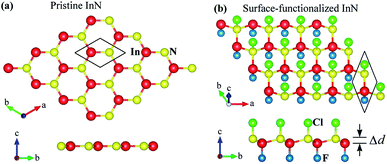 |
| | Fig. 1 Relaxed atomic structures in different views of pristine InN (a) and (b) surface-functionalized InN (b) monolayers at equilibrium. | |
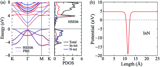 |
| | Fig. 2 Band structure and density of states (a) and electrostatic potential (b) of monolayer InN at equilibrium. The unit cells of monolayers are indicated by the rhombuses. | |
When the InN monolayer is chemically functionalized with the Cl and F atoms, the planar structure of the InN monolayer is broken and the chemically functionalized InN monolayer has a low-bucked structure as shown in Fig. 1(b). In the present work, we consider four models of the surface-functionalization of InN with the Cl and F atoms. There are fully fluorinated F–InN–F, chemically functionalization with both F and Cl atoms F–InN–Cl and Cl–InN–F, and fully chlorinated Cl–InN–Cl. The calculated structural parameters, as well as some typical parameters of all four models, are listed in Table 1. As shown in Table 1 we can see that the lattice constant of functionalized InN is larger than that of pristine InN monolayer. Also, focusing on the species, the bond lengths between the Cl and In/N atoms is always longer than that between the F and In/N atoms in all models. At equilibrium, the buckling constant of the functionalized InN monolayers vary from 0.460 Å (F–InN–F) to 0.516 Å (Cl–InN–Cl).
Table 1 Lattice constant a, bond lengths d and buckling constant Δd (Å) of pristine InN and chemically functionalized InN with F and Cl. Binding energy Eb, energy gaps Eg (PBE/PBE + SOC) and Eg (HSE/HSE + SOC) (eV), and spin–orbit splitting value ΔE (PBE/HSE) (meV) of the monolayers
| Model |
a |
dIn–N |
dIn–F |
dIn–Cl |
dN–F |
dN–Cl |
Δd |
Eb |
EPBE/PBE+SOCg |
EHSE/HSE+SOCg |
ΔEPBE/HSE |
| InN |
3.616 |
2.088 |
— |
— |
— |
— |
0 |
|
0.712/0.237 |
1.721/1.425 |
21.370/9.775 |
| F–InN–F |
3.716 |
2.194 |
1.736 |
— |
1.577 |
— |
0.460 |
−8.425 |
1.926/1.470 |
3.267/3.048 |
18.556/8.238 |
| F–InN–Cl |
3.701 |
2.195 |
1.733 |
— |
— |
1.859 |
0.505 |
−7.579 |
1.167/0.683 |
2.351/2.017 |
55.392/12.105 |
| Cl–InN–F |
3.725 |
2.201 |
— |
2.227 |
1.583 |
— |
0.468 |
−5.844 |
0.939/0.812 |
2.048/1.955 |
76.493/15.778 |
| Cl–InN–Cl |
3.711 |
2.204 |
— |
2.226 |
— |
1.865 |
0.516 |
−4.997 |
0.808/0.576 |
1.834/1.646 |
67.651/12.720 |
To check the stability of surface-functionalized InN monolayers with F and Cl atoms, we calculate their phonon spectra at equilibrium. Our calculations for the phonon dispersion curves of all configurations of surface-functionalized InN monolayers with F and Cl atoms are depicted in Fig. 3. Our obtained results for the phonon spectra of the surface-functionalized InN monolayers demonstrated that there are no soft phonon modes in the phonon dispersion curves of all four configurations of the surface-functionalized InN monolayers with F and Cl atoms. It means that at equilibrium, all four configurations of the surface-functionalized InN monolayers with F and Cl atoms are dynamically stable.
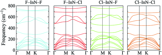 |
| | Fig. 3 Calculated phonon spectra of the surface-functionalized InN monolayers with F and Cl atoms. | |
We estimated the binding energy of the functionalized InN monolayer with the Cl and F atoms via the expression as follows
| | |
Eb = EA1–InN–A2 − (EInN + EA1 + EA2),
| (1) |
where A1 and A2 refer to the F or Cl atoms (A1 = F, Cl; A2 = F, Cl),
EInN and
EA1–InN–A2 are the total energies of the pristine InN and chemically functionalized InN with A1 and/or A2 atoms, respectively.
EA1/A2 is the haft of total energy of the fluorine (F
2) or chlorine (Cl
2) calculated in the gas form. The obtained results for the binding energy
Eb of all four models of the chemically functionalized InN with Cl and F atoms are presented in
Table 1. As shown in
Table 1, the calculated binding energies of four functionalized models are negative. It means that the adsorption of the F and Cl atoms on the surface of the InN monolayer is chemically possible. The binding energy depends strongly on the species. The binding energy of the fully fluorinated F–InN–F is the most negative (−8.425 eV). This implies that chemical adsorption on the F–InN–F model is most likely to occur.
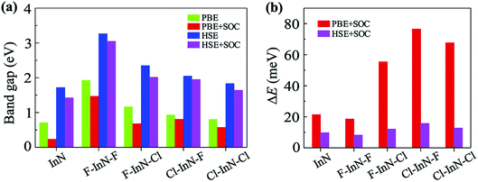
Calculated band structures of chemically functionalized InN with F and Cl atoms are depicted in Fig. 4. We can see that, for an individual model of surface functionalization, the calculated band structures at the PBE and HSE06 levels are the same profile. Our obtained results demonstrate that while the InN monolayer has an indirect gap, all models of surface-functionalized InN monolayers are direct gap semiconductors. This means that surface functionalization has led to indirect–direct gap transition in InN monolayer. By comparing Fig. 2(a) to Fig. 4, it is easy to realize that the transition is due to the shift of the VBM from the K- to the Γ-point when the InN monolayer is chemically functionalized with Cl and F atoms. Previous studies have been shown that the SOC plays an important role in the electronic properties of the 2D materials, such as monochalcogenides43 or Janus structures.44,45 Therefore, in this work, we have also included the SOC into the calculations for band structures of all configurations of the chemically functionalization of InN with Cl and F atoms. The band structures of the chemically functionalized InN monolayers by the PBE + SOC and HSE06 + SOC approaches are illustrated in Fig. 5. The obtained results demonstrate that the band gap of all configurations is significantly reduced when the SOC is included. More importantly, a small spin–orbit splitting has appeared at the Γ-point near the Fermi level in the valence band. The band gaps and the spin–orbit splitting values ΔE of the chemically functionalized InN monolayers are depicted in Fig. 6. The surface functionalization of the InN monolayer makes its band gap increase. However, depending on the species, the increase in the gap is uneven. This band gap increase due to the surface functionalization of InN monolayer is similar to the case of the gas adsorption on the surface of the InN monolayer28 or in the InN nonpolar surface functionalization.27 From Fig. 6, we can see that, compared to other configurations, the band gap of the F–InN–F monolayer is largest. It is 1.926 eV and 3.267 eV at PBE and HSE06 levels, respectively. It is well-known that the electronic properties of layered 2D materials are particularly sensitive to the structural perfection. Upon the surface-functionalization, the geometric structure of functionalized InN monolayers changes significantly, especially the In–N bond lengths, as shown in Table 1. In addition to the influence of atomic orbitals of species F and Cl, the change in geometric structure of the InN monolayer when it is functionalizated due to hybridization between the orbitals when the monolayer is functionalized by gas atoms. Also, the nature of chemical bonds in the functionalized InN monolayers can be determined by the difference of electronegativities between metallic ions and halogen anions. The change in the structure and difference in electronegativity between atoms are the main causes of changes in band gap of monolayers.
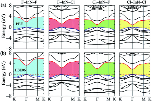 |
| | Fig. 4 Calculated band structures of surface-functionalized InN monolayers at PBE (a) and HSE06 (b) levels. | |
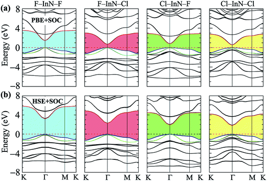 |
| | Fig. 5 Calculated band structures of surface-functionalized InN monolayers using the PBE + SOC (a) and HSE06 + SOC (b) methods. | |
 |
| | Fig. 6 Band gaps (a) and spin–orbit splitting values ΔE at Γ-point (b) of pristine InN and surface-functionalized InN monolayers. | |
When the SOC is included, the band gap of monolayers decreases. However, the reduction of each monolayer is different as shown in Fig. 6(a). The effect of the SOC on the energy gap of the pristine InN monolayer is much greater than that of functionalized InN monolayer. The calculated band gap by the PBE functional of the pristine InN monolayer when the SOC including reduces to 0.237 eV, 67% less than the pristine case (0.712 eV). In four models of the chemically functionalization of the monolayer InN with F and Cl atoms, the effect of the SOC on the PBE band gap of the F–InN–Cl is largest. The band gap of the F–InN–Cl in the cases of with and without SOC is respectively 0.683 eV and 1.167 eV, the band gap of the F–InN–Cl monolayer is reduced by 41.47% due to the influence of the SOC. Compared to the case of using the PBE method, the calculated band gap by HSE06 hybrid functional in the presence of the SOC is reduced slightly. The spin–orbit splitting values ΔE of the monolayers are also depicted in Fig. 6(b). While the spin–orbit splitting value ΔE of the F–InN–F monolayer is quite small (only 18.556 meV by the PBE + SOC approach), the ΔE value of the Cl–InN–F monolayer is largest, up to 76.493 meV. In the pristine InN monolayer, although the SOC significantly reduces its band gap, the spin–orbit splitting value ΔE generated by the SOC is very small, only 21.370 meV.
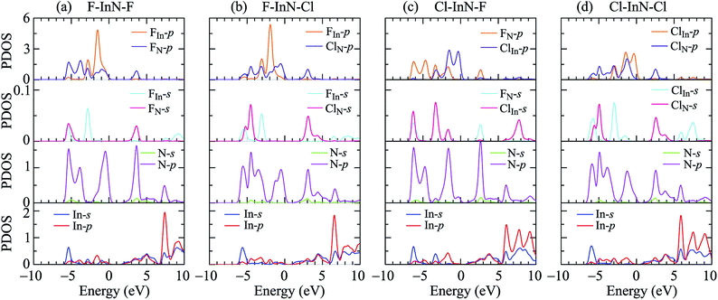
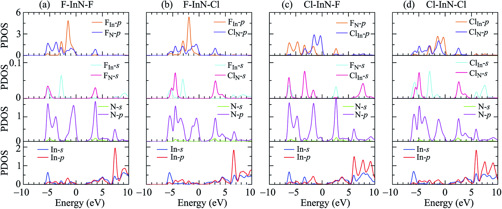
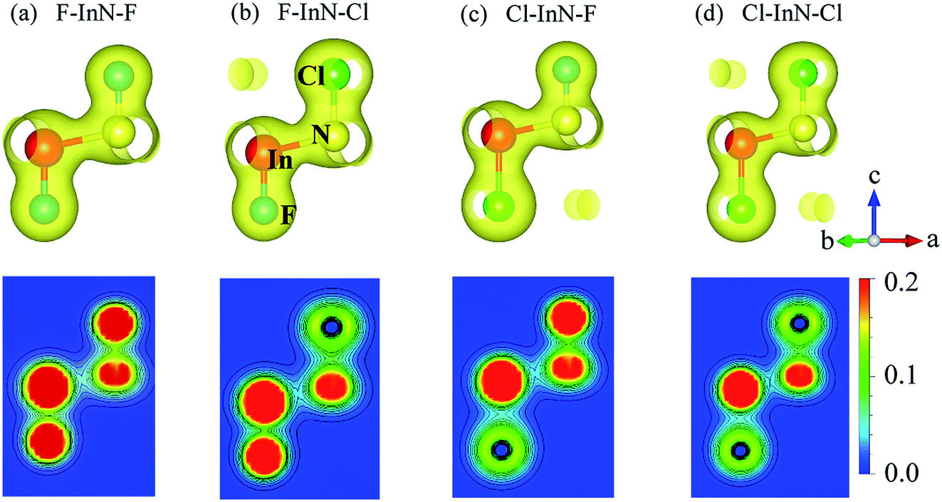
To see in detail the contribution of orbitals to the formation of electronic bands, we performed the calculations for the partial density states (PDOS) of the monolayer as illustrated in Fig. 7. The formation of the electronic is due to the major contributions from the orbitals of the N atoms. The In-p orbital has a significant contribution to the high energy region of the conduction band. Atom orbitals of the species also make a significant contribution to the formation of electronic bands of the systems, in particular to the valence band near the Fermi level. Besides, the charge density of the atoms in all models of chemically functionalized InN monolayers with F and Cl atoms is calculated as shown in Fig. 8. In all models of the chemically functionalized InN monolayers, the electron density is enriched around both In and N atoms. For functionalized species, enrichment of electron is only for the F atoms, the electronic charge distribution in Cl species is quite small. The charge transfer between atoms will be analyzed below.
 |
| | Fig. 7 The PDOS of the chemically functionalized InN monolayers: (a) F–InN–F, (b) F–InN–Cl, (c) Cl–InN–F, and (d) Cl–InN–Cl. | |
 |
| | Fig. 8 Charge density with isolated 0.04 (up panel) and contour form of electron density of atoms from 0 to 0.2 e bohr−3 with 0.02 bohr3 interval (bottom panel) of the chemically functionalized InN monolayers: (a) F–InN–F, (b) F–InN–Cl, (c) Cl–InN–F, and (d) Cl–InN–Cl. | |
We use the Mulliken population analysis46 to consider the internal charge distribution and charge transfer between InN monolayer and species in the chemically functionalized InN monolayers. In Table 2, we listed the charge distribution of the pristine InN monolayer and all models of its chemically functionalization. The total charge of the In and N atoms is respectively +1.15e and −1.15e. As listed in Table 2, one can see that the electrons have transferred from the InN layer (from In atoms) to the species. The electrons transferred from In to N and functionalized species Cl and/or F are different for different models. In the case of fully fluorinated InN monolayer F–InN–F, the transferred charge from the InN monolayer to the species (F atoms) is maximum compared to other models of chemically functionalized InN monolayers. The difference in transferred charge is due to the difference in atom electronegativity, particularly, the electronegativity of the N atom is quite larger than that of the In atoms.
Table 2 Internal charge distribution (in unit of e) by Mulliken population analysis in pristine InN and chemically functionalized InN monolayers. The last column shows the charge transfer between InN and Cl/F species. Cl(F)In and Cl(F)N stand for the species Cl(F) directly linked to In and N atoms, respectively
| Model |
s |
p |
Total |
Charge |
Transferred charge |
| InN |
In |
1.75 |
4.4 |
6.15 |
+1.15 |
— |
| N |
0.85 |
1.00 |
1.85 |
−1.15 |
|
| F–InN–F |
FIn |
1.97 |
3.89 |
5.68 |
−0.68 |
+0.96 |
| In |
0.61 |
0.75 |
1.36 |
+1.64 |
|
| N |
1.79 |
3.89 |
5.68 |
−0.68 |
|
| FN |
1.98 |
5.33 |
7.31 |
−0.31 |
|
| F–InN–Cl |
FIn |
1.96 |
5.68 |
7.64 |
−0.64 |
+0.67 |
| In |
0.62 |
0.79 |
1.41 |
+1.59 |
|
| N |
1.80 |
4.12 |
5.92 |
−0.92 |
|
| ClN |
1.95 |
5.08 |
7.03 |
−0.03 |
|
| Cl–InN–F |
ClIn |
1.95 |
5.45 |
7.40 |
−0.31 |
+0.71 |
| In |
0.74 |
0.91 |
1.65 |
+1.35 |
|
| N |
1.79 |
3.85 |
5.64 |
−0.64 |
|
| FN |
1.98 |
5.34 |
7.31 |
−0.31 |
|
| Cl–InN–Cl |
ClIn |
1.95 |
5.44 |
7.39 |
−0.39 |
+0.43 |
| In |
0.75 |
0.95 |
1.70 |
+1.30 |
|
| N |
1.80 |
4.08 |
5.87 |
−0.87 |
|
| ClN |
1.80 |
4.08 |
5.87 |
−0.87 |
|
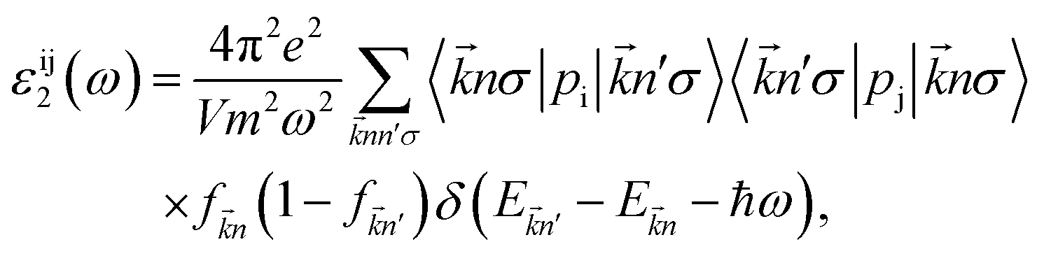
In the next, we will investigate on the optical characteristics of the chemically functionalized InN monolayer with the Cl and F atoms. In this work, only on the dielectric function ε(ω), the absorption coefficient α(ω) and optical reflectivity R(ω) are considered. The dielectric function is given by
| | |
ε(ω) = ε1(ω) + iε2(ω),
| (2) |
where
ε2(
ω) is the imaginary part which is usually derived first by sum of the transitions between the occupied and unoccupied states and we can then get the real part
ε1(
ω) throught the Kramer–Kronig transformation. The
ε2(
ω) can be given by
47,48| |
 | (3) |
where
ω is the electromagnetic irradiation angular-frequency,
m(
e) refers to the mass (charge) of the electron,

and

stand respectively for the momentum operator and the wave-vector,

term refers to the wave-function of the crystal corresponding to energy

and

is the Fermi distribution.
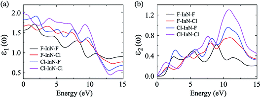
In our calculations, the incoming light is polarized along the a-axis with energy range from 0 eV to 15 eV (parallel polarization). The dielectric function parts of the chemically functionalized InN monolayers with the Cl and F atoms are illustrated in Fig. 9. Our simulated results demonstrate that while the first optical gaps of the F–InN–F and Cl–InN–F monolayers are in the energy of the visible light region, the first optical gaps of the F–In–Cl and Cl–InN–Cl monolayers are in the infrared region. Focusing on the imaginary part ε2(ω) as shown in Fig. 9(b), we can see that the first optical gaps of the F–InN–F and Cl–InN–F monolayers are at 2.500 eV and 2.725 eV of the incident light energy, respectively. This implies that the F–InN–F and Cl–InN–F monolayers have a strong ability to absorb the visible light.
 |
| | Fig. 9 Real ε1(ω) (a) and imaginary ε2(ω) (b) parts of the dielectric function of the chemically functionalized InN monolayers with Cl and F atoms. | |
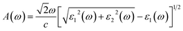
The absorption coefficient A(ω) and the optical reflectivity R(ω) can be defined via the dielectric function which is given by48,49
| |
 | (4) |
and
| |
 | (5) |
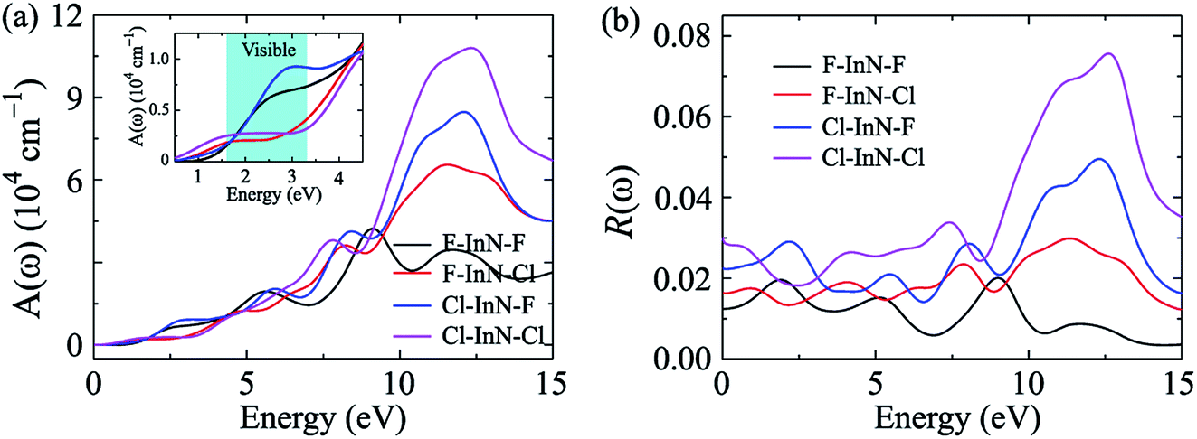
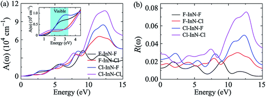
The absorption coefficient A(ω) and the optical reflectivity R(ω) of the chemically functionalized InN monolayers with Cl and F atoms as a function of the incoming light energy are depicted in Fig. 10. As shown in Fig. 10(a), one can see that the chemically functionalized InN monolayer with Cl and F atoms is capable of absorbing light in a wide range, from the infrared to the ultraviolet. While the F–InN–Cl and Cl–InN–Cl monolayers can absorb the light even in the infrared region as above-mentioned, the F–InN–F and Cl–InN–F monolayers strongly absorbs the visible light. The maximum absorption coefficient A(ω)max of the monolayers is in the ultraviolet region. The fully chlorinated InN monolayer has the highest absorption coefficient. The A(ω)max for the Cl–InN–Cl monolayer is up to 10.779 × 104 cm−1 at the incoming light energy of 12.430 eV. Focusing on the visible light regions as shown in the inset in Fig. 10(a), we can see that the F–InN–F and Cl–InN–F monolayers can strongly absorb the visible light. The first optical gap in the Cl–InN–F monolayer is in the visible light region at the energy of 3.103 eV and the absorption coefficient for the Cl–InN–F monolayer at 3.103 eV is 0.923 × 104 cm−1. As shown in Fig. 10(b), the optical reflectivity R(ω) of the chemically functionalized InN monolayers with Cl and F atoms has a high intensity in the ultraviolet region. In the energy region of the incoming light from 0 to 25 eV, the Cl–InN–F monolayer has highest optical reflectivity R(ω). We believe that with its ability to absorb light in a wide range, especially the F–InN–F and Cl–InN–F monolayers which strongly absorb the visible light, will make the chemically functionalized InN monolayers with Cl and F atoms a potential material for applications in nano optoelectronic devices.
 |
| | Fig. 10 Absorption coefficient A(ω) (a) and optical reflectivity R(ω) (b) of chemically functionalized InN monolayers with Cl and F atoms. Inset in (a) is to clearly show the A(ω) in the visible light region. | |
4 Conclusion
In conclusion, the structural, electronic and optical properties of the chemically functionalized InN monolayers are systematically investigated from density functional theory. The adsorption of the F and Cl atoms on the InN monolayer is determined to be chemically stable due to the analysis of their adsorption energies. All four models of the chemically functionalization of InN monolayer with F and Cl atoms are direct band gap semiconductors. For individual functionalized InN monolayer, the calculated band structures by PBE and HSE06 functional are the same profile and the band gap is reduced when the SOC is included. The chemically functionalized InN monolayers, particularly the F–InN–F and Cl–InN–F monolayers, have a high absorption coefficient in the visible light region, which has promising applications in optoelectronic devices. Our results may motivate experimental studies on the surface-functionalization of 2D materials in the future.
Conflicts of interest
There are no conflicts to declare.
Acknowledgements
This research is funded by Vietnam National Foundation for Science and Technology Development (NAFOSTED) under Grant No. 103.01-2018.334.
References
- K. S. Novoselov, D. Jiang, F. Schedin, T. J. Booth, V. V. Khotkevich, S. V. Morozov and A. K. Geim, Proc. Natl. Acad. Sci. U. S. A., 2005, 102, 10451 CrossRef CAS PubMed.
- M. Yarmohammadi, RSC Adv., 2017, 7, 10650 RSC.
- H. Şahin, S. Cahangirov, M. Topsakal, E. Bekaroglu, E. Aktürk, R. T. Senger and S. Ciraci, Phys. Rev. B: Condens. Matter Mater. Phys., 2009, 80, 155453 CrossRef.
- C. E. P. Villegas and A. R. Rocha, J. Phys. Chem. C, 2015, 119, 11886 CrossRef CAS.
- M. S. Prete, A. Mosca Conte, P. Gori, F. Bechstedt and O. Pulci, Appl. Phys. Lett., 2017, 110, 012103 CrossRef.
- M. S. Prete, O. Pulci and F. Bechstedt, Phys. Rev. B, 2018, 98, 235431 CrossRef CAS.
- P. T. T. Le, M. Davoudiniya and M. Yarmohammadi, Phys. Chem. Chem. Phys., 2019, 21, 238 RSC.
- M. Yarmohammadi, J. Magn. Magn. Mater., 2017, 426, 621 CrossRef CAS.
- M. Yarmohammadi, AIP Adv., 2016, 6, 085008 CrossRef.
- R. Ruoff, Nat. Nanotechnol., 2008, 3, 10 CrossRef CAS PubMed.
- Y. Qu, H. Pan and C. T. Kwok, Sci. Rep., 2016, 6, 34186 CrossRef CAS PubMed.
- T. V. Vu, N. T. T. Anh, D. Hoat, D. P. Tran, H. D. Tong, H. L. Luong, L. M. Hieu, C. V. Nguyen, H. V. Phuc, N. T. Binh and N. N. Hieu, Phys. E, 2020, 117, 113857 CrossRef.
- Y. Zhang, H. Ye, Z. Yu, H. Gao and Y. Liu, RSC Adv., 2018, 8, 7022 RSC.
- Y. Jiao, F. Ma, J. Bell, A. Bilic and A. Du, Angew. Chem., Int. Ed., 2016, 55, 10292 CrossRef CAS PubMed.
- R. Balog, B. Jørgensen, L. Nilsson, M. Andersen, E. Rienks, M. Bianchi, M. Fanetti, E. Lægsgaard, A. Baraldi, S. Lizzit, Z. Sljivancanin, F. Besenbacher, B. Hammer, T. G. Pedersen, P. Hofmann and L. Hornekær, Nat. Mater., 2010, 9, 315 CrossRef CAS PubMed.
- J. Son, S. Lee, S. J. Kim, B. C. Park, H.-K. Lee, S. Kim, J. H. Kim, B. H. Hong and J. Hong, Nat. Commun., 2016, 7, 13261 CrossRef CAS PubMed.
- T. Pakornchote, Z. M. Geballe, U. Pinsook, T. Taychatanapat, W. Busayaporn, T. Bovornratanaraks and A. F. Goncharov, Carbon, 2020, 156, 549 CrossRef CAS.
- W. Feng, P. Long, Y. Feng and Y. Li, Adv. Sci., 2016, 3, 1500413 CrossRef PubMed.
- W. Kang and S. Li, RSC Adv., 2018, 8, 23459 RSC.
- M. J. Park, J. K. Lee, B. S. Lee, Y.-W. Lee, I. S. Choi and S.-g. Lee, Chem. Mater., 2006, 18, 1546 CrossRef CAS.
- D. Bouša, J. Luxa, V. Mazánek, O. Jankovský, D. Sedmidubský, K. Klímová, M. Pumera and Z. Sofer, RSC Adv., 2016, 6, 66884 RSC.
- H. Şahin and S. Ciraci, J. Phys. Chem. C, 2012, 116, 24075 CrossRef.
- L. Yang, K. Majumdar, H. Liu, Y. Du, H. Wu, M. Hatzistergos, P. Y. Hung, R. Tieckelmann, W. Tsai, C. Hobbs and P. D. Ye, Nano Lett., 2014, 14, 6275 CrossRef CAS PubMed.
- M.-E. Ragoussi, G. Katsukis, A. Roth, J. Malig, G. de la Torre, D. M. Guldi and T. Torres, J. Am. Chem. Soc., 2014, 136, 4593 CrossRef CAS PubMed.
- V. Z. Poenitzsch, D. C. Winters, H. Xie, G. R. Dieckmann, A. B. Dalton and I. H. Musselman, J. Am. Chem. Soc., 2007, 129, 14724 CrossRef CAS PubMed.
- T. Hu and I. C. Gerber, J. Phys. Chem. C, 2013, 117, 2411 CrossRef CAS.
- A. Terentjevs, G. Cicero and A. Catellani, J. Phys. Chem. C, 2009, 113, 11323 CrossRef CAS.
- X. Sun, Q. Yang, R. Meng, C. Tan, Q. Liang, J. Jiang, H. Ye and X. Chen, Appl. Surf. Sci., 2017, 404, 291 CrossRef CAS.
- J. M. Zavada, R. G. Wilson, C. R. Abernathy and S. J. Pearton, Appl. Phys. Lett., 1994, 64, 2724 CrossRef CAS.
- C.-F. Chen, C.-L. Wu and S. Gwo, Appl. Phys. Lett., 2006, 89, 252109 CrossRef.
- K. A. Rickert, A. B. Ellis, F. J. Himpsel, H. Lu, W. Schaff, J. M. Redwing, F. Dwikusuma and T. F. Kuech, Appl. Phys. Lett., 2003, 82, 3254 CrossRef CAS.
- H. Lee, M. L. Cohen and S. G. Louie, Appl. Phys. Lett., 2010, 97, 233101 CrossRef.
- H. Pan, Y. P. Feng and J. Y. Lin, J. Phys.: Condens. Matter, 2006, 18, 5175 CrossRef CAS.
- P. E. Blöchl, Phys. Rev. B: Condens. Matter Mater. Phys., 1994, 50, 17953 CrossRef PubMed.
- P. Giannozzi, S. Baroni, N. Bonini, M. Calandra, R. Car, C. Cavazzoni, D. Ceresoli, G. L. Chiarotti, M. Cococcioni, I. Dabo, A. D. Corso, S. de Gironcoli, S. Fabris, G. Fratesi, R. Gebauer, U. Gerstmann, C. Gougoussis, A. Kokalj, M. Lazzeri, L. Martin-Samos, N. Marzari, F. Mauri, R. Mazzarello, S. Paolini, A. Pasquarello, L. Paulatto, C. Sbraccia, S. Scandolo, G. Sclauzero, A. P. Seitsonen, A. Smogunov, P. Umari and R. M. Wentzcovitch, J. Phys.: Condens. Matter, 2009, 21, 395502 CrossRef PubMed.
- J. P. Perdew, K. Burke and M. Ernzerhof, Phys. Rev. Lett., 1996, 77, 3865 CrossRef CAS PubMed.
- J. P. Perdew, K. Burke and M. Ernzerhof, Phys. Rev. Lett., 1997, 78, 1396 CrossRef CAS.
- A. H. MacDonald, W. E. Picket and D. D. Koelling, J. Phys. C: Solid State Phys., 1980, 13, 2675 CrossRef CAS.
- J. P. Perdew and M. Levy, Phys. Rev. Lett., 1983, 51, 1884 CrossRef CAS.
- J. Heyd, G. E. Scuseria and M. Ernzerhof, J. Chem. Phys., 2003, 118, 8207 CrossRef CAS.
- S. Grimme, J. Comput. Chem., 2006, 27, 1787 CrossRef CAS.
- L. Hedin, Phys. Rev., 1965, 139, A796 CrossRef.
- D. Pandey and A. Chakrabarti, Phys. Lett. A, 2019, 383, 2914–2921 CrossRef CAS.
- S.-D. Guo, X.-S. Guo, R.-Y. Han and Y. Deng, Phys. Chem. Chem. Phys., 2019, 21, 24620 RSC.
- T. V. Vu, H. D. Tong, D. P. Tran, N. T. T. Binh, C. V. Nguyen, H. V. Phuc, H. M. Do and N. N. Hieu, RSC Adv., 2019, 9, 41058 RSC.
- R. S. Mulliken, J. Chem. Phys., 1955, 23, 1833 CrossRef CAS.
- A. Delin, P. Ravindran, O. Eriksson and J. Wills, Int. J. Quantum Chem., 1998, 69, 349 CrossRef CAS.
- S. Z. Karazhanov, P. Ravindran, A. Kjekshus, H. Fjellvag and B. G. Svensson, Phys. Rev. B: Condens. Matter Mater. Phys., 2007, 75, 155104 CrossRef.
- P. Ravindran, A. Delin, B. Johansson, O. Eriksson and J. M. Wills, Phys. Rev. B: Condens. Matter Mater. Phys., 1999, 59, 1776 CrossRef CAS.
|
| This journal is © The Royal Society of Chemistry 2020 |
Click here to see how this site uses Cookies. View our privacy policy here. 
 Open Access Article
 This Open Access Article is licensed under a Creative Commons Attribution-Non Commercial 3.0 Unported Licence
 ab,
Khang D. Phamcd,
Tri Nhut Pham
ab,
Khang D. Phamcd,
Tri Nhut Pham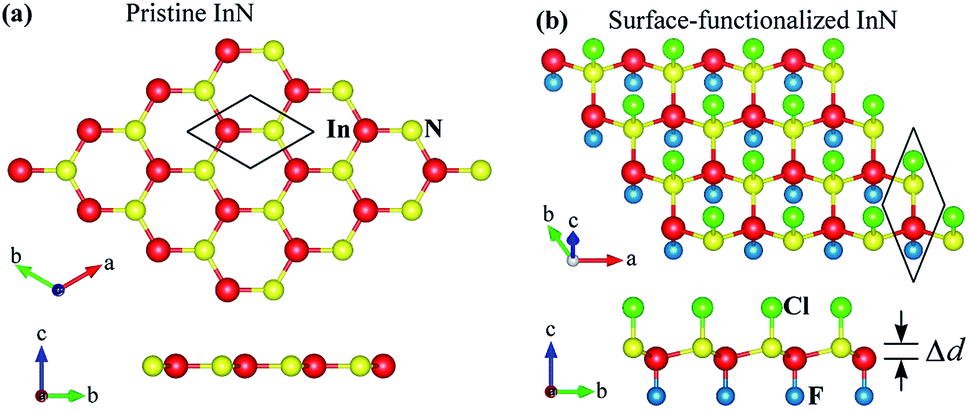


 and
and  stand respectively for the momentum operator and the wave-vector,
  term refers to the wave-function of the crystal corresponding to energy
  and
and  is the Fermi distribution.