DOI:
10.1039/D0RA00734J
(Paper)
RSC Adv., 2020,
10, 16088-16093
A high-throughput synthesis of large-sized single-crystal hexagonal boron nitride on a Cu–Ni gradient enclosure
Received
23rd January 2020
, Accepted 1st April 2020
First published on 23rd April 2020
Abstract
Large monolayer two-dimensional h-BN can be employed in novel electronic devices because of its thin insulation, excellent thermal stability, and high mechanical strength. However, the efficient synthesis of an h-BN film with large lateral size still faces a great challenge. Here, we report a method for the high-throughput synthesis of large-sized single-crystal h-BN on a Cu–Ni gradient alloy enclosure as the substrate via a low-pressure chemical vapor deposition (LPCVD) method. By depositing Ni on the Cu foil in different concentrations to obtain a Cu–Ni in-plane gradient concentration alloy enclosure, the highest growth rate of h-BN was 1 μm min−1 with the lateral size of h-BN being higher than 60 μm. Furthermore, the effect of the Ni content on the single crystal h-BN grain size and nucleation density and the mechanisms for the growth of h-BN were also investigated.
1. Introduction
Two-dimensional hexagonal boron nitride (h-BN) has excellent thermal stability, good thermal conductivity and electrical insulation, unique UV luminescence, high mechanical strength, and dielectric properties. Hence, it is widely used in optoelectronic devices, dielectric materials, multi-functional coating materials, and self-cleaning devices. By the ion beam sputtering deposition method, Wang et al. obtained the single-crystal h-BN with a lateral size of 110 μm on polycrystalline Ni foils.1 Furthermore, using the same method, Meng et al. realized the aligned growth of single-crystal h-BN with a lateral size of 600 μm on epitaxial Ni (111)/sapphire substrates.2 By the sonication-assisted hydrothermal exfoliation, Tian et al. obtained high crystalline boron nitride nanosheets.3 In addition, the chemical vapor deposition (CVD) method is the most promising method to acquire the h-BN film with high quality and large area. Wang et al. realized the epitaxial growth of the unidirectionally aligned single-crystal h-BN on a low-symmetry Cu (110) substrate by the LPCVD method.4 Tay et al. reduced the nucleation point of h-BN by electrolytically polishing the copper substrate and obtained h-BN crystal domains with an area of 35 μm2.5 Song et al. used a Cu envelope as the substrate and obtained the h-BN film, with a lateral size of 72 μm and a growth rate of 0.4 μm min−1.6 Ji et al. used a copper enclosure with a copper foil thickness of 127 μm and obtained monolayer h-BN domains with a lateral size up to 300 μm.7 Ying et al. used ammonia borane as a precursor and obtained the h-BN domain a size up to ∼22 μm on a Pt foil, which was inserted into a Cu enclosure with a Ni foam.8 Among the above studies, few literatures aimed at increasing the growth rate of h-BN. We summarized the correlation between the lateral size and the growth rate of single-crystal h-BN reported in a previous study, as shown in Fig. 1.5–7,9–22 It is in order to grow h-BN with a higher growth rate and simultaneously guarantee the lateral size.
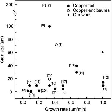 |
| | Fig. 1 The figure of size and growth rate of single crystal h-BN on a Cu foil and copper envelope. | |
As it was reported that decreasing the precursor feeding rate can suppress the nucleation of h-BN,6 so two strategies were incorporated to reduce the amount of boron and nitrogen radicals appearing on the substrate surface. On the one hand, we used the Cu–Ni alloy enclosure as the substrate, where the enclosure was confirmed to suppress the diffusion of boron and nitrogen radicals into the inner surface of the enclosure.6,7 On the other hand, we found that the existence of the Ni atom in the Cu–Ni alloy enclosure can further suppress this diffusion. More importantly, the introduction of Ni can enhance the decomposition of the ammonia borane, which is used as a precursor,8,23 thus improving the growth rate of h-BN. Therefore, in this study, we tried to develop an efficient method of reducing the nucleation density of h-BN to increase the grain size with a high growth rate via LPCVD. The mechanism for the growth of h-BN was also investigated.
2. Experimental detail
2.1 Preparation of Cu–Ni alloy enclosure
A 35 μm-thick copper foil (99.5%, Alfa Aesar) was cut into 80 mm × 35 mm pieces, pre-cleaned by ultrasonication in glacial acetic acid (AR) and de-ionized (DI) water. Then, the Ni film was deposited on the Cu foil with the current density of 0.5 A cm−2 via electroplating. An electrolytic solution consisted of NiSO4·6H2O (320 g), NiCl2·6H2O (48 g), H3BO3 (40 g), and water (1 L). To obtain the Cu–Ni alloy with an in-plane gradient concentration of Ni, the rectangle copper foil was lifted with a vertical length of ∼5 mm per 20 s from the electrolytic solution in the process of electroplating. The atomic ratio of Ni of the Cu–Ni alloy was measured by EDS and ranged from 2% to 12%. After electroplating, the Ni/Cu foil was folded into a sealed enclosure. The details of enclosure fabrication are shown in Fig. 2(a). After annealing, the three-folded edges were sealed entirely, which was testified by the cross-section SEM images shown in Fig. 2(a).
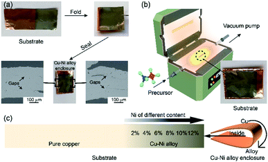 |
| | Fig. 2 (a) Preparation progress of the Cu–Ni alloy enclosure and the cross-section SEM images. (b) Schematic of the LPCVD system. (c) Schematic of the Cu–Ni alloy with the gradient concentration of Ni. | |
2.2 Synthesis and transfer of the h-BN film
As is shown in Fig. 2(b), the LPCVD system was used for the h-BN deposition. The Ni/Cu alloy enclosure was loaded into a CVD-fused quartz tube with a diameter of 40 mm. 10–20 mg of ammonia borane was used as the precursor. To make the two metals inter-diffuse completely to generate the Cu–Ni alloy, the enclosure was annealed at 1060 °C in a mixed Ar/H2 (500/50 sccm) flow under atmospheric pressure for 1 h before growth. After annealing, the mixed Ar/H2 flow was changed to 80/20 sccm at the temperature of 1060 °C, and the h-BN grew at a pressure of 100 Pa with the growth time of 60 min. Meanwhile, the precursor was heated to 95 °C using a water bath. To further characterize the structure of h-BN, the samples were transferred to a SiO2/Si substrate or a TEM grid. This study used the bubbling transfer process, and the process was consistent with the transfer of graphene. The details can be found in ref. 24.
2.3 Characterization
The microstructure of h-BN was observed by optical microscopy (OM, MX6RT, Sunny Optical Technology Co.) in a reflection mode and scanning electron microscopy (SEM, FEI Quanta-FEG250 at 20 kV). Atomic force microscopy (AFM) imaging was performed using a Bruker Multimode 8 DI in a contact mode. The high-resolution transmission electron microscopy (HRTEM) combined with the selected area electron diffraction (SAED) was carried out using a JEM-2100 (JEOL, Tokyo, Japan) at 200 kV. Raman spectroscopy (Horiba LabRam HR800 Ev, 532 nm) and X-ray photoelectron spectroscopy (XPS, ESCALAB 250Xi, Thermo Fischer) were used to confirm the existence of h-BN.
3. Results and discussion
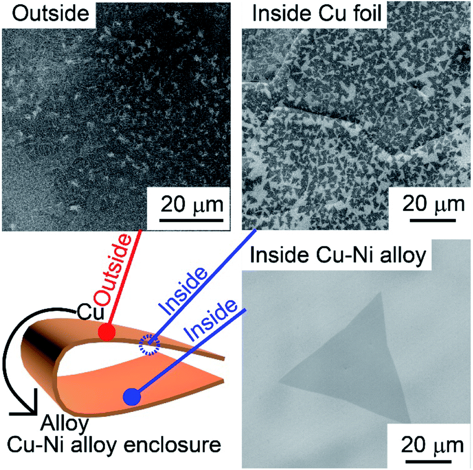
Fig. 3 shows the SEM images of the h-BN morphology on the outside of the enclosure, the Cu foil, and Cu–Ni alloy inside of the enclosure, respectively. The substrate fully covered with small h-BN flakes was observed outside the enclosure, whereas the single-crystal h-BN with different sizes was observed inside the enclosure. It is obvious that the nucleation density of h-BN on the inner enclosure was reduced greatly. As for the inner surface of the enclosure, when the size and nucleation density of h-BN deposited on the Cu foil and Cu–Ni alloy were compared, the nucleation density was found to be ∼4.4 × 10⁵ nuclei per mm2 on the pure copper foil and the largest h-BN domain size was only 1–2 μm, while the nucleation density was reduced to ∼1.0 × 10² nuclei per mm2 on the Cu–Ni alloy and the domain size was increased to ∼60 μm. Upon further increasing the growth time, the h-BN would continue to grow until it touched the adjacent grain. The doped Ni atoms make a great reduction in the nucleation density of h-BN on the Cu foil. This phenomenon is consistent with the previous work, which states that the nucleation density of the h-BN growth on the Cu–Ni alloy can decrease enormously as the introduction of Ni can enhance the decomposition of the ammonia borane.23 However, there is neither poly-ammonia-borane nor its partially dehydrogenated derivatives on the inner surface of the Cu–Ni alloy enclosure, which is correlated to the h-BN grain nucleation. It is apparent that the reduction in the nucleation density is due to other mechanisms, which will be described below.
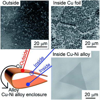 |
| | Fig. 3 The SEM images of h-BN film on the outside of the enclosure, the Cu foil, and Cu–Ni alloy inside of the enclosure, respectively. | |
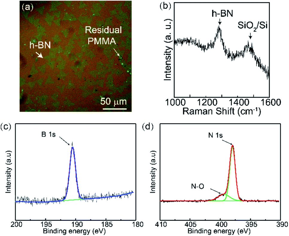
Fig. 4(a) shows the OM image of the triangular single-crystal h-BN on the SiO2/Si substrate. The XPS spectra (Fig. 4(b) and (c)) show that the binding energies of B 1s and N 1s were 190.54 eV and 398.24 eV, respectively. The ratio of B to N atom was 1. This result is consistent with that obtained in the previous literature, confirming the existence of the B–N bond.22 A Raman characteristic peak is found at 1368 cm−1 in Fig. 4(d), which corresponds to the h-BN E2g phonon frequency. The small peak at 1450 cm−1 is from the third-order transverse optical (TO) phonon mode of Si, which is also observed on the pure SiO2/Si substrate.
 |
| | Fig. 4 (a) OM image of single crystal h-BN on a 300 nm thick SiO2/Si substrate. (b) Raman spectrum of h-BN on the 300 nm thick SiO2/Si substrate. (c and d) XPS spectra of B 1s and N 1s. | |
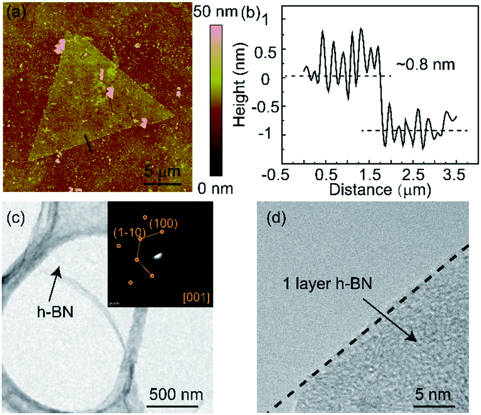
AFM was used to measure the thickness of the h-BN film. The single-crystal h-BN with a typical triangular shape is observed in the AFM image (Fig. 5(a)). Moreover, Fig. 5(b) shows that the thickness of h-BN is ∼0.8 nm, which is consistent with a monolayer thickness on Si/SiO2. To further characterize the crystalline and the layer number of h-BN, the TEM images are shown in Fig. 5(c) and (d). The insert of Fig. 5(c) shows the SAED pattern of h-BN. A set of characteristic six-fold symmetric spots of the h-BN film is observed, which confirm the good crystallinity of the h-BN grains. The high-resolution TEM image is shown in Fig. 5(d), which further proves the mono-layer of the h-BN film.
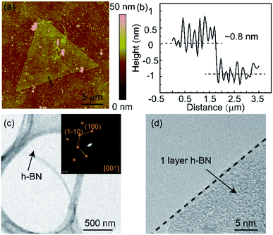 |
| | Fig. 5 (a and b) AFM image of monolayer h-BN and the height profile along the black line. (c) Low magnification TEM image of the h-BN film on a carbon-coated copper grid. The insert shows the SAED pattern of a random region of the h-BN film. (d) HRTEM image of a mono-layer h-BN film. | |
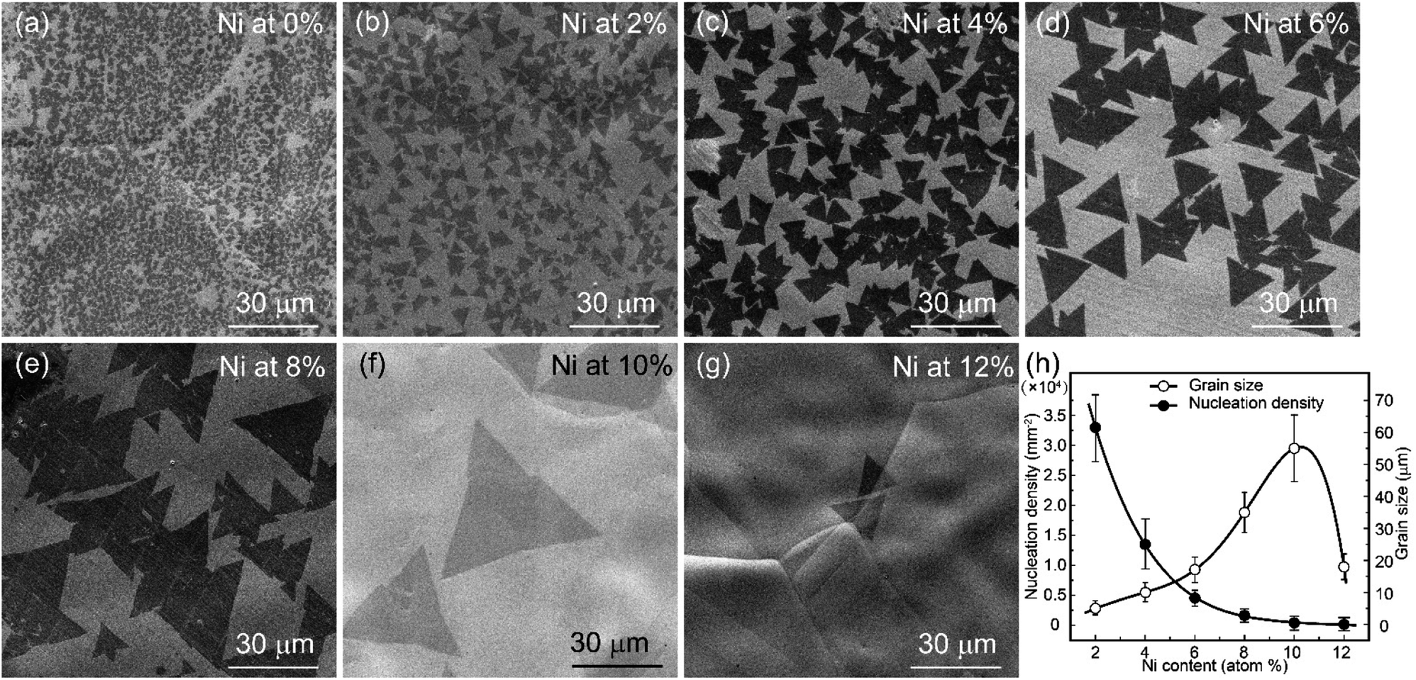
Fig. 6 shows the influence of the Ni content on the single-crystal h-BN grain size and nucleation density. The nucleation density of h-BN deposited on pure Cu (Fig. 6(a)) was up to 4 × 105 mm−2, and the corresponding grains size was just 1–2 μm. When the Ni atom was doped into the Cu foil, the nucleation density of h-BN decreased greatly. The SEM images of h-BN deposited on different Ni contents (2–12%) are shown in Fig. 6(b)–(g). Moreover, the relationship between the grain size/nucleation density and the Ni content is shown in Fig. 6(h). When the Ni content is at 10%, the single-crystal h-BN grains size increased to ∼60 μm with a high lateral growth rate of 1 μm min−1, and the nucleation density reduced to 400 mm−2. With a further increase in the Ni content (12%), the nucleation density decreased to 100 mm−2, but the grain size was only ∼30 μm at a lower lateral growth rate of ∼0.5 μm min−1. That is to say, the high content of Ni can suppress the formation of h-BN. This phenomenon is consistent with the law discovered by the previous work,23 and the different suppress mechanisms are discussed as follows.
 |
| | Fig. 6 (a–g) The SEM image of h-BN grown on the Cu–Ni alloy foils with different Ni contents (a) 0%, (b) 2%, (c) 4%, (d) 6%, (e) 8%, (f) 10%, and (g) 12% at 1060 °C for 60 min. (h) Dependence of the single crystal h-BN grain size and nucleation density on the Ni content. | |
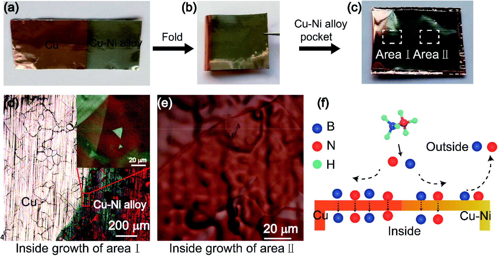
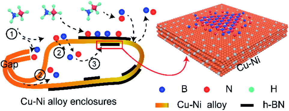
Fig. 7 shows the growth mechanisms of h-BN on the inner Cu–Ni enclosures. Kong and Ruoff et al. have discussed the growth mechanism of graphene on the Cu enclosures.25,26 They thought that the carbon atoms have two pathways to diffuse into the inner surface of the enclosure. Ji et al. had investigated the mechanism of h-BN on the Cu enclosures.7 They had proved that when the copper envelope was completely sealed, the B and N atoms could only diffuse into the interior of the envelope through bulk diffusion. Unlike their studies, we used a Cu–Ni alloy folded into an enclosure. The two possible diffusion pathways of precursor between the inner and outer enclosure are as follow: (1) gaps of three edges and (2) the Cu–Ni alloy bulk. The three folded edges were sealed completely after annealing, which could be confirmed by the cross-section images. Compared to the Cu enclosure, we found that the Cu–Ni enclosures have another function: the existence of Ni atoms can further prevent the diffusion of boron and nitrogen radicals into the inner surface. The preparation process of the Cu–Ni enclosure is shown in Fig. 7(a)–(c). The Ni film with a certain concentration was deposited on the Cu foil and then turned into Cu–Ni alloy after annealing. Fig. 7(d) and (e) show the growth of h-BN at the inner surface of the enclosure, which corresponds to area I and area II in Fig. 7(c), respectively. With a certain amount of precursor and growth time, it can be seen that a continuous h-BN film was formed on the copper foil, the sporadic h-BN domain was formed at the boundary between Cu and Cu–Ni alloy area, and no h-BN was generated on the Cu–Ni alloy. When the amount of precursor or the growth time was increased, a separate h-BN domain with a larger grain size was observed on the inner surface of the Cu–Ni alloy; and a continuous film was formed on the inner Cu foil. This phenomenon shows that the incorporation of the Ni atom in the Cu foil can block B, N atom diffusion into the inner surface of the enclosure. Fig. 7(f) is the schematic of the B and N atom diffusion into the interior of the enclosure through pure Cu and Cu–Ni alloy. The Cu–Ni alloy prevents the excess precursor from entering the inside of the enclosure by blocking or absorbing the B and N atoms, thereby the nucleation density of h-BN was reduced greatly. The schematic of the growth mechanism of h-BN on the inner Cu–Ni enclosure is shown in Fig. 8. When ammonia borane decomposes at a high temperature, B and N atoms diffuse into the inner surface of the enclosure by bulk diffusion only, excess precursor atoms are blocked by the copper-nickel alloy, which greatly reduces the nucleation density on the interior surface and grows single-crystal h-BN with a large size. In addition, the introduction of Ni can enhance the decomposition of the ammonia borane on the outer surface of the Cu–Ni alloy enclosure, thus improving the growth rate of h-BN.
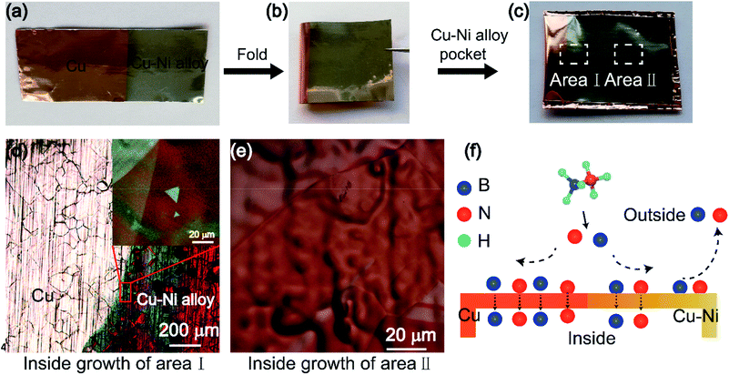 |
| | Fig. 7 (a–c) Preparation progress of the Cu–Ni alloy pocket; (d and e) Optical picture of area I and area II in (c), the inset is the magnified optical image of h-BN corresponding to the region marked by the red square; (f) schematic of atoms diffusing into the interior of the pocket through pure copper and Cu–Ni alloy bulk. | |
 |
| | Fig. 8 Schematic of the growth mechanism of h-BN on inner Cu–Ni enclosures. (1) Decomposition, (2) diffusion, (3) the nucleation and growth of h-BN. | |
4. Conclusion
In conclusion, we synthesized a large single-crystal h-BN film with a lateral size of 60 μm and the growth rate of 1 μm min−1 on the Cu–Ni alloy enclosure, compared with h-BN with a lateral size of 1–2 μm deposited on pure copper. The as-grown crystal h-BN was a monolayer, with a thickness of 0.8 nm and a lateral size of ∼20 μm, which was further confirmed by the HRTEM image. The growth mechanism of h-BN on the inner surface of the enclosure was discussed. Besides, the high-throughput synthesis of h-BN was realized by depositing the Ni film, with a gradient concentration on the Cu foil with the optimal Ni content of 10%.
Conflicts of interest
There are no conflicts to declare.
Acknowledgements
This work was supported by the Science Challenge Project (No. TZ2016001), the National Natural Science Foundation of China (No. 51861145306, 51872212 and 51972244), and the 111 Project (B13035), and Joint Fund of Ministry of Education for Pre-research of Equipment (6141A02022257). This research was also supported by the International Science & Technology Cooperation Program of China (2018YFE0103600, 2014DFA53090), the Technological Innovation of Hubei Province, China (2019AAA030), the Fundamental Research Funds for the Central Universities (WUT: 2018YS003, 2018YS016, 2019III030, 2019III028, SCU: YJ201893), and the State Key Laboratory of Advanced Technology for Materials Synthesis and Processing (WUT, Grant No. 2019-KF-12) and State Key Lab of Advanced Metals and Materials, China (Grant No. 2019-Z03).
Notes and references
- H. L. Wang, X. W. Zhang, H. Liu, Z. G. Yin, J. H. Meng, J. Xia, X. M. Meng, J. L. Wu and J. B. You, Adv. Mater., 2015, 27, 8109–8115 CrossRef CAS PubMed.
- J. H. Meng, X. W. Zhang, Y. Wang, Z. G. Yin, H. Liu, J. Xia, H. L. Wang, J. B. You, P. Jin, D. G. Wang and X. M. Meng, Small, 2017, 13, 8 CrossRef PubMed.
- Z. Tian, K. Chen, S. Sun, J. Zhang, W. Cui, Z. Xie and G. Liu, J. Adv. Ceram., 2019, 8, 72–78 CrossRef CAS.
- L. Wang, X. Z. Xu, L. N. Zhang, R. X. Qiao, M. H. Wu, Z. C. Wang, S. Zhang, J. Liang, Z. H. Zhang, Z. B. Zhang, W. Chen, X. D. Xie, J. Y. Zong, Y. W. Shan, Y. Guo, M. Willinger, H. Wu, Q. Y. Li, W. L. Wang, P. Gao, S. W. Wu, Y. Zhang, Y. Jiang, D. P. Yu, E. G. Wang, X. D. Bai, Z. J. Wang, F. Ding and K. H. Liu, Nature, 2019, 570, 91–95 CrossRef CAS PubMed.
- R. Y. Tay, M. H. Griep, G. Mallick, S. H. Tsang, R. S. Singh, T. Tumlin, E. H. Teo and S. P. Karna, Nano Lett., 2014, 14, 839–846 CrossRef CAS PubMed.
- X. Song, J. Gao, Y. Nie, T. Gao, J. Sun, D. Ma, Q. Li, Y. Chen, C. Jin, A. Bachmatiuk, M. H. Rümmeli, F. Ding, Y. Zhang and Z. Liu, Nano Res., 2015, 8, 3164–3176 CrossRef CAS.
- Y. Ji, B. Calderon, Y. Han, P. Cueva, N. R. Jungwirth, H. A. Alsalman, J. Hwang, G. D. Fuchs, D. A. Muller and M. G. Spencer, ACS Nano, 2017, 11, 12057–12066 CrossRef CAS PubMed.
- H. Ying, X. T. Li, D. S. Li, M. Q. Huang, W. Wan, Q. Yao, X. P. Chen, Z. W. Wang, Y. Q. Wu, L. Wang and S. S. Chen, 2D Mater., 2018, 5, 9 Search PubMed.
- R.-J. Chang, X. Wang, S. Wang, Y. Sheng, B. Porter, H. Bhaskaran and J. H. Warner, Chem. Mater., 2017, 29, 6252–6260 CrossRef CAS.
- J. Yin, J. Yu, X. Li, J. Li, J. Zhou, Z. Zhang and W. Guo, Small, 2015, 11, 4497–4502 CrossRef CAS PubMed.
- Y. Stehle, H. M. Meyer, R. R. Unocic, M. Kidder, G. Polizos, P. G. Datskos, R. Jackson, S. N. Smirnov and I. V. Vlassiouk, Chem. Mater., 2015, 27, 8041–8047 CrossRef CAS.
- X. Song, Q. Li, J. Ji, Z. Yan, Y. Gu, C. Huo, Y. Zou, C. Zhi and H. Zeng, 2D Mater., 2016, 3, 035007 CrossRef.
- S. Sharma, K. Sharma, M. S. Rosmi, Y. Yaakob, M. I. Araby, H. Ohtani, G. Kalita and M. Tanemura, Cryst. Growth Des., 2016, 16, 6440–6445 CrossRef CAS.
- N. Guo, J. Wei, L. Fan, Y. Jia, D. Liang, H. Zhu, K. Wang and D. Wu, Nanotechnology, 2012, 23, 415605 CrossRef PubMed.
- L. Wang, B. Wu, L. Jiang, J. Chen, Y. Li, W. Guo, P. Hu and Y. Liu, Adv. Mater., 2015, 27, 4858–4864 CrossRef CAS PubMed.
- G. E. Wood, A. J. Marsden, J. J. Mudd, M. Walker, M. Asensio, J. Avila, K. Chen, G. R. Bell and N. R. Wilson, 2D Mater., 2015, 2, 025003 CrossRef.
- S. Sharma, G. Kalita, R. Vishwakarma, Z. Zulkifli and M. Tanemura, Sci. Rep., 2015, 5, 10426 CrossRef PubMed.
- R. Y. Tay, X. Wang, S. H. Tsang, G. C. Loh, R. S. Singh, H. Li, G. Mallick and E. H. Tong Teo, J. Mater. Chem. C, 2014, 2, 1650–1657 RSC.
- K. K. Kim, A. Hsu, X. Jia, S. M. Kim, Y. Shi, M. Hofmann, D. Nezich, J. F. Rodriguez-Nieva, M. Dresselhaus, T. Palacios and J. Kong, Nano Lett., 2012, 12, 161–166 CrossRef PubMed.
- C. Wu, A. M. Soomro, F. Sun, H. Wang, C. Liu, X. Yang, J. Kang and D. Cai, Phys. Status Solidi B, 2016, 253, 829–833 CrossRef CAS.
- R. Y. Tay, H. Li, S. H. Tsang, M. Zhu, M. Loeblein, L. Jing, F. N. Leong and E. H. T. Teo, Chem. Mater., 2016, 28, 2180–2190 CrossRef CAS.
- L. Wang, B. Wu, J. Chen, H. Liu, P. Hu and Y. Liu, Adv. Mater., 2014, 26, 1559–1564 CrossRef CAS PubMed.
- G. Lu, T. Wu, Q. Yuan, H. Wang, H. Wang, F. Ding, X. Xie and M. Jiang, Nat. Commun., 2015, 6, 6160 CrossRef CAS PubMed.
- C. Zhang, R. Tu, M. Dong, J. Li, M. Yang, Q. Li, J. Shi, H. Li, H. Ohmori, S. Zhang, L. Zhang and T. Goto, Carbon, 2019, 150, 356–362 CrossRef CAS.
- W. Fang, A. L. Hsu, Y. Song, A. G. Birdwell, M. Amani, M. Dubey, M. S. Dresselhaus, T. Palacios and J. Kong, ACS Nano, 2014, 8, 6491–6499 CrossRef CAS PubMed.
- Y. Hao, L. Wang, Y. Liu, H. Chen, X. Wang, C. Tan, S. Nie, J. W. Suk, T. Jiang, T. Liang, J. Xiao, W. Ye, C. R. Dean, B. I. Yakobson, K. F. McCarty, P. Kim, J. Hone, L. Colombo and R. S. Ruoff, Nat. Nanotechnol., 2016, 11, 426–431 CrossRef CAS PubMed.
|
| This journal is © The Royal Society of Chemistry 2020 |
Click here to see how this site uses Cookies. View our privacy policy here. 
 Open Access Article
 This Open Access Article is licensed under a Creative Commons Attribution-Non Commercial 3.0 Unported Licence
 b,
Mingdong Dong
b,
Mingdong Dong