
 Open Access Article
 This Open Access Article is licensed under a Creative Commons Attribution-Non Commercial 3.0 Unported Licence
Colloidal quantum dot light-emitting diodes employing solution-processable tin dioxide nanoparticles in an electron transport layer
Myeongjin Parka,
Jiyun Songa,
Myungchan Anb,
Jaehoon Limc,
Changhee Lee a,
Jeongkyun Roh*d and
Donggu Lee*b
a,
Jeongkyun Roh*d and
Donggu Lee*b
aDepartment of Electrical and Computer Engineering, Inter-university Semiconductor Research Center, Seoul National University, Seoul 08826, Republic of Korea
bRealistic Media Research Center, Innovative Technology Research Division, Gumi Electronics & Information Technology Research Institute (GERI), Gumi 39253, Republic of Korea. E-mail: dglee@geri.re.kr
cDepartment of Energy Science, Center for Artificial Atoms, Sungkyunkwan University (SKKU), Suwon-Si, Gyeonggi-do 16419, Republic of Korea
dDepartment of Electrical Engineering, Pusan National University, Busan, 46241, Republic of Korea. E-mail: jkroh@pusan.ac.kr
First published on 26th February 2020
Abstract
Colloidal quantum-dot-based light-emitting diodes (QD-LEDs) have gained tremendous attention as great candidates to potentially replace current emissive display technologies. The luminescence efficiency of a QD LED has increased rapidly in the past decade; this was triggered by the use of metal oxides in the charge transport layers, particularly zinc oxide (ZnO) for the electron transport layer (ETL). However, the ZnO ETL often results in undesirable device performance such as efficiency roll-off and poor device stability because of excessive electron injection into the QD emissive layer. Here, we explore solution-processable tin dioxide (SnO2) nanoparticles (NPs) as alternatives to ZnO NPs for the ETL in QD-LEDs. We evaluated the thin-film quality and electrical performance of SnO2 NPs and then applied them to the ETL for constructing QD-LEDs. As a result of the smooth surface morphology, moderate electron-transport ability, and lower carrier concentration compared to ZnO NPs, the QD-LED with SnO2 NP-ETL exhibited improved performance in terms of lower turn-on and operating voltages, maximum luminance, improved efficiency roll-off, and improved power efficiency over the reference device with the ZnO NP-ETL. This shows promising potential for SnO2 NPs in optoelectronic applications.
Introduction
Colloidal quantum dots (QDs) are considered a key material for next-generation displays because of their excellent optical properties such as tunable emission wavelength, high color purity, and high photoluminescence (PL) quantum yield.1–3 These unique features have enabled successful commercialization of QD display technologies based on color enhancement films. Intense research works are presently underway as the next step toward replacement of current emissive displays by QD light-emitting diodes (QD-LEDs). Luminescence efficiency is one of the most important factors in the commercialization of QD-LEDs. Through careful studies on the design of QDs, the PL quantum yield has almost reached 100%, indicating high technological advancement in QD synthesis.4,5 Simultaneously, several studies have been conducted to achieve high luminescence efficiency from an electroluminescence (EL) device via optimum device architecture. This involves finding suitable materials for the charge transport layers (CTLs) and charge injection layers (CILs) of electrons and holes, and various types of organic/inorganic nanomaterials have been employed and investigated.6–8 Among these materials, zinc oxide (ZnO) nanoparticles (NPs) have been most frequently employed as electron transport layers (ETLs) because of their excellent electron mobilities and suitable energy levels for efficient electron injection.9–11 Although ZnO ETLs are widely employed and considered a standard platform for high-efficiency QD-LEDs, ZnO has been often indicated as the main reason for undesirable behavior of QD-LED performance such as efficiency roll-off, EL quenching, and short lifetime.12–14 These behaviors are attributable to excessive electron injection from ZnO into the QDs, which lead to non-balancing of electron and hole densities in the QD emissive layer.15 To move one step closer to commercialization, it is currently necessary to study other alternatives that can potentially supplement or even replace ZnO.In this study, we explore tin dioxide (SnO2) NPs as possible alternatives to ZnO NPs for ETLs in QD-LEDs. SnO2 NPs are solution-processable n-type semiconductors similar to ZnO NPs and can form transparent and smooth thin films at temperatures below 100 °C. SnO2 NPs. In addition, they possess a wider bandgap with less sensitivity in the ultraviolet regime than ZnO, indicating better light stability.16 Because of their superior features, SnO2 have been often employed in perovskite photovoltaics as an alternative of TiO2,17–19 but utilization of SnO2 in LEDs has not been performed. To test the suitability of SnO2 NPs for ETLs, we first evaluated the thin-film quality of SnO2 NPs using atomic force microscopy (AFM) measurements, and confirmed that SnO2 NPs form uniform thin films without notable valleys. Then, we investigated the electrical properties of SnO2 NPs, such as electron mobility and carrier concentration, by employing a field-effect transistor (FET) as a test platform. Finally, we constructed QD-LEDs based on an inverted structure using SnO2 NPs for the ETL, evaluated the device performance, and compared it to that of QD-LEDs with the ZnO NP-ETL.
Experimental
Materials
The SnO2 NPs dispersed in water (>99.5%) was purchased from MKnano and used as received. The synthetic procedure for ZnO nanoparticles and CdSe/CdS/CdZnS red QDs followed a reported method by Kawk et al.9 Precursors for synthesizing QDs and ZnO nanoparticles (zinc acetate dehydrate > 99%, tributylphosphine > 99%, 1-octadecene > 95%, trioctylphosphine > 97%, oleic acid > 99%) were purchased from Sigma-Aldrich, and potassium hydroxide (>85%) was purchased from Duksan Pharmaceutical Co. Ltd.Characterization of ZnO and SnO2 films
An Agilent 8454 UV-visible spectrometer was used for UV-vis absorption. An XE-100 (Park Systems Corp.) AFM system was used to analyze the topography of the ZnO NPs and SnO2 NP films. The transmission electron microscopy (TEM) images of the ZnO and SnO2 NPs were taken with a JEOL JSM-890 at an accelerating voltage of 120 kV.Fabrication and characterization of FETs based on metal oxide NPs
Heavily doped silicon and thermally grown 300 nm SiO2 were used as a gate and gate dielectric, respectively. The Si/SiO2 substrates were cleaned in an ultra-sonication bath with acetone, isopropyl alcohol, and de-ionized water, sequentially. Then, the substrates were stored in a vacuum oven for 10 min to remove moisture. Before depositing metal-oxide NPs, the substrates were UVO-treated for 10 min, and then ZnO or SnO2 NPs were spin-coated onto the substrates. Then, the metal oxide NP films were annealed at 90 °C for 30 min to remove residual solvents. A shadow mask was used to form source and drain electrodes by thermally evaporating 0.5 nm LiF and 100 nm Al, sequentially. The channel width and length of the FETs were 65 μm and 1800 μm, respectively. The electrical performance of metal-oxide NP-based FETs were measured using a semiconductor parameter analyzer, Agilent 4155C.Fabrication and characterization of QD-LEDs
Patterned ITO glass substrates were sequentially ultrasonicated with acetone, isopropanol, and deionized water for at least 5 minutes. Then, the cleaned substrates were dried in an oven at 120 °C for at least 30 min. To deposit the electron injection layer, a SnO2 NP solution (15 mg mL−1 dispersed in deionized water) and a ZnO NP solution (20 mg mL−1 in butanol) were spin-casted on the substrate, respectively, at 2000 rpm for 60 s. The coated films were baked in a N2 oven at 90 °C for 30 min, and the thickness measured with an ellipsometer was 40 nm. After baking, a 20 mg mL−1 QD solution in hexane was spin-casted on top of the ETL at 4000 rpm for 30 s, and then baked again in the N2 oven at 70 °C for 30 min to form a 20 nm emissive layer. Finally, the substrates were transferred to a vacuum evaporator, and then 40 nm CBP for the hole transport layer (HTL), 10 nm MoO3 for the hole injection layer (HIL) and 100 nm Al for the anode were thermally evaporated with a deposition rate of 1 A s−1. The current density–voltage–luminance (J–V–L) characteristics were measured using a Keithley 236 source-measurement unit and calibrated Si photodiode (Hamamatsu, S5227-1010BQ). During the J–V measurement, luminance was obtained by correcting the photocurrent of the Si photodiode with a luminance value measured by a spectroradiometer (Konica-Minolta CS-1000A).Results and discussion
Fig. 1 shows a schematic illustration of inverted-structure QD-LEDs with ETLs consisting of metal-oxide NPs. The metal-oxide NPs used in this study, ZnO and SnO2, had a similar size of ∼3–5 nm as shown in the TEM images in Fig. 1. In this inverted structure, metal-oxide NPs were deposited on the bottom ITO electrode, and QDs were deposited on top of the metal-oxide NP ETLs. Thus, it is extremely important to have high-quality metal-oxide NP films because (i) the morphology of the QD emissive layer follows the morphology of the underlying ETL; and (ii) pinholes or cracks present in the ETL result in the direct contact of QDs with the bottom electrode which yields a massive leakage current. To evaluate the thin-film quality of SnO2 NPs, we performed AFM measurements for both SnO2 and ZnO NP films and compared them accordingly.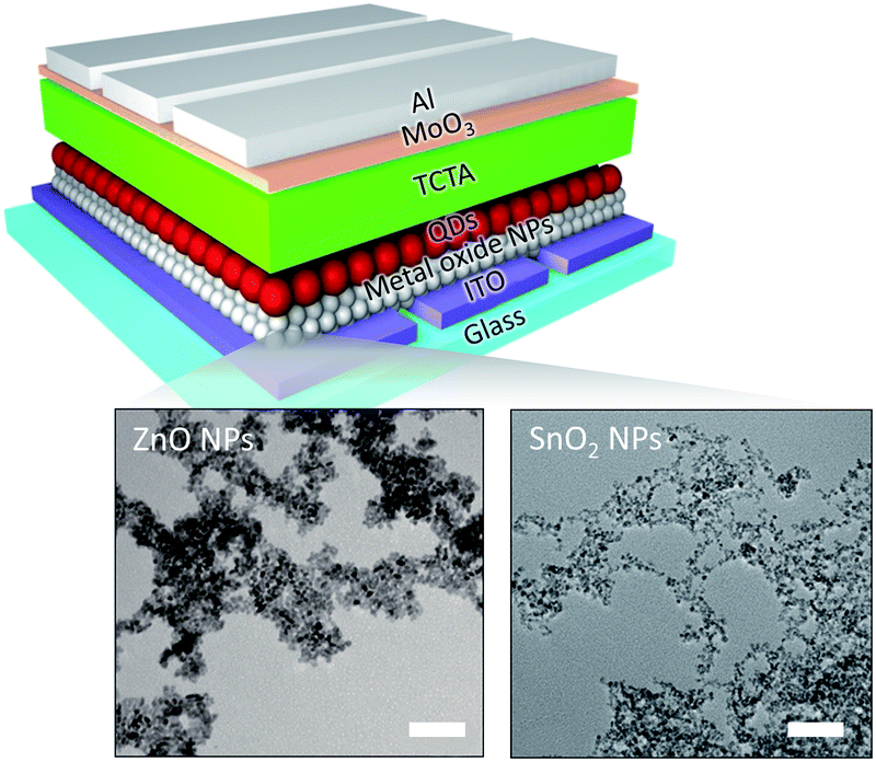 | ||
| Fig. 1 Schematic illustration of the QD-LED based on an inverted structure with an ETL consisting of metal-oxide NPs. Bottom inset shows TEM images of metal-oxide NPs used in this study. The scale bars represent 50 nm. | ||
Fig. 2(a) and (b) show the surface morphology of the thin films consisting of ZnO and SnO2 NPs, respectively. As shown, SnO2 NPs produce a smooth, thin film without notable cracks or a valleys, similar to ZnO NPs. The surface roughness of the SnO2 NP film measured by rms over the 5 μm × 5 μm area is 2.8 nm, which is lower than that of the ZnO NP film (3.9 nm). The high smoothness of the SnO2 NP film is a favorable feature for ETLs, which is linked to a lower leakage current, high EL efficiency (i.e., a uniform emissive layer), maximum luminescence (i.e., high breakdown voltage), and high device stability.
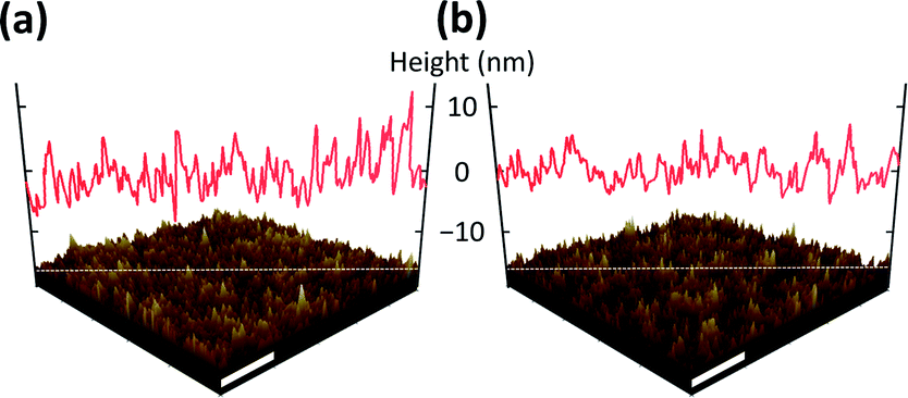 | ||
| Fig. 2 AFM surface morphologies of thin films consisting of (a) ZnO NPs and (b) SnO2 NPs along with their surface profiles. The scale bars represent 1 μm. | ||
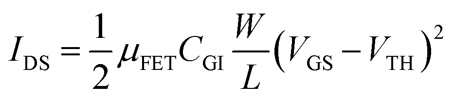
After confirming the high film quality of the SnO2 NPs, we evaluated its electrical properties using an FET platform. An FET is a representative electronic device that can amplify or switch signals; it is also a useful platform with which to evaluate the electrical properties of semiconductors. As shown in Fig. 3(a), we fabricated bottom-gate top-contact FETs using ZnO or SnO2 NPs as the channel material. Fig. 3(b) shows the transfer characteristics of the FETs based on ZnO and SnO2 NPs in a saturation regime with a drain-to-source voltage (VDS) of 100 V. The electron mobility and threshold voltage can be extracted from the equation,
 | (1) |
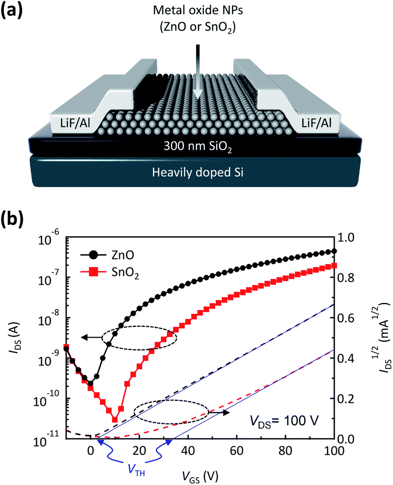 | ||
| Fig. 3 (a) Device structure of FETs based on metal-oxide NPs. (b) Saturation-regime transfer characteristics of FETs based on ZnO and SnO2 NPs. The blue arrows indicate x-intercepts which represent threshold voltages of each device. | ||
Finally, we fabricated QD-LEDs based on the SnO2 NP-ETL as shown in Fig. 1. In this study, we employed CdSe/CdS/CdZnS red QDs with a high PL quantum yield of approximately 80%. Fig. 4(a) shows an energy diagram of the QD-LEDs with ETLs consisting of ZnO or SnO2 NPs. As displayed in the figure, electrons injected from ITO pass through metal oxide NPs and arrive at the QD emissive layer, indicating that metal-oxide NPs play a significant role in both electron injection and transport. Fig. 4(b) shows the EL spectra of QD-LEDs with ZnO or SnO2 NP-ETLs. The luminance–voltage–current density (L–V–J) measurements show that the QD-LED with the SnO2 NP-ETL exhibits comparable or even slightly improved performance over the ZnO NP ETL-based device. Besides, the device with the SnO2 NP-ETL shows a low driving voltage in the J–V curve compared to the ZnO NP-ETL device, denoting its suitability as an electron injection/transport layer. As a result, the device with the SnO2 NP-ETL has a lower turn-on voltage (VON ∼ 2.15 V) and higher maximum luminance (Lmax ∼ 15![[thin space (1/6-em)]](https://www.rsc.org/images/entities/char_2009.gif) 000 cd m−2) than the ZnO NP-ETL based device (VON ∼ 2.35 V, Lmax ∼ 10000 cd m−2). Furthermore, as shown in Fig. 4(d), the QD-LED with the SnO2 NP-ETL exhibits improved external quantum efficiency (EQE) roll-off behavior with a peak EQE of 3.9% and power efficiency (PE) compared to the ZnO NP-ETL based device. This shows the excellent performance of the SnO2 NPs for the ETL in QD-LEDs; this is attributable to the high thin-film quality, comparable electron mobility, and lower carrier concertation, which could suppress spontaneous electron injection.
000 cd m−2) than the ZnO NP-ETL based device (VON ∼ 2.35 V, Lmax ∼ 10000 cd m−2). Furthermore, as shown in Fig. 4(d), the QD-LED with the SnO2 NP-ETL exhibits improved external quantum efficiency (EQE) roll-off behavior with a peak EQE of 3.9% and power efficiency (PE) compared to the ZnO NP-ETL based device. This shows the excellent performance of the SnO2 NPs for the ETL in QD-LEDs; this is attributable to the high thin-film quality, comparable electron mobility, and lower carrier concertation, which could suppress spontaneous electron injection.
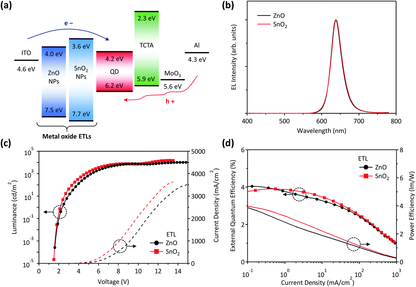 | ||
| Fig. 4 (a) Energy diagram of QD-LEDs with metal-oxide NP-based ETLs. (b) EL spectra, (c) L–V–J characteristics, and (d) EQE and PE characteristics of devices with ZnO NP- and SnO2 NP-ETLs. | ||
Conclusions
In summary, we examined SnO2 NPs for the ETL in QD-LEDs as a possible alternative to ZnO NPs. The high thin-film quality of the SnO2 NPs is a favorable feature for ETL in preventing leakage current pathways, and its electrical performance, including the moderate electron mobility and lower carrier concentration than ZnO NPs, is desirable for the ETL in QD-LEDs. As a result, the QD-LEDs based on the SnO2 NP-ETL show compatible or even improved device performance over the device to those with the ZnO NP-ETL; this indicates the promising potential of SnO2 NPs as a supplement or an alternative to ZnO NPs. This work is expected to expand the utilization of SnO2 NPs in optoelectronic applications and promote exploration of other types of metal-oxide NPs.Conflicts of interest
There are no conflicts to declare.Acknowledgements
This work was supported by the Ministry of Education of the Republic of Korea and the National Research Foundation of Korea (NRF-2019R1C1C1005258).Notes and references
- Y.-H. Won, O. Cho, T. Kim, D.-Y. Chung, T. Kim, H. Chung, H. Jang, J. Lee, D. Kim and E. Jang, Nature, 2019, 575, 634–638 CrossRef CAS PubMed.
- H. Shen, Q. Gao, Y. Zhang, Y. Lin, Q. Lin, Z. Li, L. Chen, Z. Zeng, X. Li, Y. Jia, S. Wang, Z. Du, L. S. Li and Z. Zhang, Nat. Photonics, 2019, 13, 192–197 CrossRef CAS.
- P. O. Anikeeva, J. E. Halpert, M. G. Bawendi and V. Bulović, Nano Lett., 2009, 9, 2532–2536 CrossRef CAS PubMed.
- D. A. Hanifi, N. D. Bronstein, B. A. Koscher, Z. Nett, J. K. Swabeck, K. Takano, A. M. Schwartzberg, L. Maserati, K. Vandewal, Y. van de Burgt, A. Salleo and A. P. Alivisatos, Science, 2019, 363, 1199 CrossRef CAS PubMed.
- B. G. Jeong, Y.-S. Park, J. H. Chang, I. Cho, J. K. Kim, H. Kim, K. Char, J. Cho, V. I. Klimov, P. Park, D. C. Lee and W. K. Bae, ACS Nano, 2016, 10, 9297–9305 CrossRef CAS PubMed.
- J. M. Caruge, J. E. Halpert, V. Wood, V. Bulović and M. G. Bawendi, Nat. Photonics, 2008, 2, 247–250 CrossRef CAS.
- M. D. Ho, D. Kim, N. Kim, S. M. Cho and H. Chae, ACS Appl. Mater. Interfaces, 2013, 5, 12369–12374 CrossRef CAS PubMed.
- V. Wood, M. J. Panzer, J. E. Halpert, J. M. Caruge, M. G. Bawendi and V. Bulović, ACS Nano, 2009, 3, 3581–3586 CrossRef CAS PubMed.
- J. Kwak, W. K. Bae, D. Lee, I. Park, J. Lim, M. Park, H. Cho, H. Woo, D. Y. Yoon, K. Char, S. Lee and C. Lee, Nano Lett., 2012, 12, 2362–2366 CrossRef CAS PubMed.
- Q. Sun, Y. A. Wang, L. S. Li, D. Wang, T. Zhu, J. Xu, C. Yang and Y. Li, Nat. Photonics, 2007, 1, 717–722 CrossRef CAS.
- X. Dai, Z. Zhang, Y. Jin, Y. Niu, H. Cao, X. Liang, L. Chen, J. Wang and X. Peng, Nature, 2014, 515, 96–99 CrossRef CAS PubMed.
- Y. Lee, B. G. Jeong, H. Roh, J. Roh, J. Han, D. C. Lee, W. K. Bae, J.-Y. Kim and C. Lee, Adv. Quantum Technol., 2018, 1, 1700006 CrossRef.
- Y. Sun, Y. Jiang, H. Peng, J. Wei, S. Zhang and S. Chen, Nanoscale, 2017, 9, 8962–8969 RSC.
- J. Pan, C. Wei, L. Wang, J. Zhuang, Q. Huang, W. Su, Z. Cui, A. Nathan, W. Lei and J. Chen, Nanoscale, 2018, 10, 592–602 RSC.
- W. K. Bae, Y.-S. Park, J. Lim, D. Lee, L. A. Padilha, H. McDaniel, I. Robel, C. Lee, J. M. Pietryga and V. I. Klimov, Nat. Commun., 2013, 4, 2661 CrossRef PubMed.
- H. Lee, C.-M. Kang, M. Park, J. Kwak and C. Lee, ACS Appl. Mater. Interfaces, 2013, 5, 1977–1981 CrossRef CAS PubMed.
- M. Kam, Q. Zhang, D. Zhang and Z. Fan, Sci. Rep., 2019, 9, 6963 CrossRef PubMed.
- V. K. Sangwan, M. Zhu, S. Clark, K. A. Luck, T. J. Marks, M. G. Kanatzidis and M. C. Hersam, ACS Appl. Mater. Interfaces, 2019, 11, 14166–14174 CrossRef CAS PubMed.
- X. Xu, Z. Xu, J. Tang, X. Zhang, L. Zhang, J. Wu and Z. Lan, Chem. Eng. J., 2018, 351, 391–398 CrossRef CAS.
- L.-C. Liu, J.-S. Chen, J.-S. Jeng and W.-Y. Chen, ECS J. Solid State Sci. Technol., 2013, 2, Q59–Q64 CrossRef CAS.
| This journal is © The Royal Society of Chemistry 2020 |