
 Open Access Article
 This Open Access Article is licensed under a Creative Commons Attribution-Non Commercial 3.0 Unported Licence
A pressure-assisted annealing method for high quality CsPbBr3 film deposited by sequential thermal evaporation†
Jingchen
Hua
a,
Xi
Deng
 a,
Cheng
Niu
a,
Fuzhi
Huang
a,
Yong
Peng
a,
Wangnan
Li
*b,
Zhiliang
Ku
*ab and
Yi-bing
Cheng
ac
a,
Cheng
Niu
a,
Fuzhi
Huang
a,
Yong
Peng
a,
Wangnan
Li
*b,
Zhiliang
Ku
*ab and
Yi-bing
Cheng
ac
aState Key Laboratory of Advanced Technologies for Materials Synthesis and Processing, International School of Materials Science and Engineering, Wuhan University of Technology, 122 Luoshi Road, Wuhan, Hubei, P. R. China. E-mail: zhiliang.ku@whut.edu.cn
bHubei Key Laboratory of Low Dimensional Optoelectronic Material and Devices, Hubei University of Arts and Science, 296 Longzhong Road, Xiangyang, Hubei Province, P. R. China
cDepartment of Materials Science and Engineering, Monash University, Wellington Road, Clayton, VIC3800, Australia
First published on 2nd March 2020
Abstract
All-inorganic CsPbBr3 perovskite solar cells have triggered incredible interest owing to their superior stability, especially under high temperature conditions. Different from the organic–inorganic hybrid perovskites, inorganic CsPbBr3 perovskite always need a high annealing temperature for the formation of a cubic phase. Generally, the higher temperature (over 300 °C) and longer annealing time will promote the growth of CsPbBr3, resulting in larger grain sizes and lower trap density in the crystals. However, CsPbBr3 perovskite can also be damaged by excessive annealing temperature (∼350 °C) and time, since PbBr2 only has a melting temperature close to 357 °C. To address this issue, herein, we developed a novel pressure-assisted annealing method to prevent the sublimation of PbBr2 at high temperature. The CsPbBr3 films were firstly deposited by sequential thermal evaporation, and then annealed at 335 °C in an alloy pressure vessel. By controlling the pressure of the vessel, we obtained CsPbBr3 films with various morphologies. At normal atmospheric pressure, the as-prepared CsPbBr3 film exhibited small grain sizes and was full of pinholes. With the increase of annealing pressure, the grain sizes of the film showed a significant increasing trend, and the pinholes gradually vanished. When the pressure value came to 10 MPa, compact and uniform CsPbBr3 films with large grain sizes were obtained. Based on these films, CsPbBr3 perovskite solar cells with FTO/compact-TiO2/CsPbBr3/carbon architecture achieved a champion power conversion efficiency of 7.22%.
Introduction
In recent years, the metal halide perovskites have attracted enormous attention due to their extraordinary optical and electronic properties.1–3 These unique features render such perovskite materials promising candidates for various optoelectronic devices, especially for solar cells. Till now, the record power conversion efficiency (PCE) of organic–inorganic hybrid perovskite solar cells (PSCs) has reached 25.2%,4 which is on par with monocrystalline silicon solar cell. However, the organic components in hybrid perovskites might be a major constraint to the commercialization of PSCs, owing to their intrinsic instability under conditions such as heat,5,6 electric field7,8 and light illumination.9–11 It should be noted that all of these conditions will not change even if the solar devices are well encapsulated. To break this impasse, more and more researchers shift their attentions toward all-inorganic perovskite,12,13 which with inorganic Cs ion in place of the organic methylammonium or formamidinium cations. CsPbI3 perovskite with a bandgap of 1.73 eV is suitable for capturing enough sunlight, and could reach 28.9% theoretical PCE according to the Shockley–Queisser limit.14 To date, a record PCE of 19.03% has been reported in the FTO/compact-TiO2/CsPbI3/spiro-OMeTAD/Ag architecture.15 However, the desired black cubic phase of CsPbI3 perovskite is only stable at high temperature over 300 °C, and spontaneously transforms to the yellow orthorhombic phase under ambient environment.16 Several strategies have been explored to stable the black cubic phase of CsPbI3 perovskite at room temperature, including of decreasing the crystal size,17 ion doping18 and surface modification.19 But still, the phase stability of CsPbI3 perovskite is far away to meet the requirement for practical applications.Full-brominated CsPbBr3 perovskite presents an yellow orthorhombic phase at room temperature and transforms to a tetragonal phase at 88 °C and to the orange cubic phase at 130 °C.20 Thanks to the wide band gap up to 2.3 eV, CsPbBr3 perovskite can maintain most of its light absorption capability during phase transition from cubic to orthorhombic. Thus, CsPbBr3-PSCs have presented excellent moisture- and thermal-tolerance even in 95% RH and 100 °C respectively.21 Despite CsPbBr3 perovskite has a wide band gap, the high electron mobility and long electron life time22 still make it become an idea light absorber. A high PCE of 10.9% (ref. 23) has been achieved in solar device with an architecture of FTO/compact-TiO2/CsPbBr3/spiro-OMeTAD/Ag. Moreover, the high open-circuit voltage (1.62 V)24 together with the high transmittance in the visible region make such CsPbBr3-PSCs to have significant potential for using in semitransparent building-integrated photovoltaics (BIPV) and tandem solar cells.25 Unfortunately, for most of the high-performance CsPbBr3-PSCs, solution-based techniques are still the first choice for the preparation of high quality CsPbBr3 films.26 Because of the poor solubility of CsBr in common solvents, CsBr always need several times coating on PbBr layer to obtain a desired CsPbBr3 film thickness.27 Obviously, the repetition of such solution-processing would be an obstacle for the reproducibility of large-area, uniform CsPbBr3 film. In this regard, vacuum deposition is a more advantageous method for depositing films with large-size and good uniformity. But at present, there are few studies on the fabrication of CsPbBr3-PSCs by using vacuum thermal evaporation.28–32 In our previous work,33,34 we demonstrated that introducing moderate moisture into the annealing process can help the crystallization of CsPbBr3 perovskite. Actually, for CsPbBr3 film deposited by sequential single-source vacuum deposition, the CsBr can hardly diffuse in the film to react properly with PbBr2 in completely “dry condition”. Hence, developing new annealing method to promote the growth of CsPbBr3 in inert atmosphere is of great significance, especially for the vacuum process.
In this work, we annealed the vacuum-deposited CsPbBr3 film in an alloy pressure vessel at 335 °C. To investigate how pressure affects the crystallization of CsPbBr3 perovskite, we adjusted the vessel pressure value from 2 MPa to 10 MPa by controlling the compressed argon gas. As a contrast, CsPbBr3 also annealed at 335 °C under standard atmospheric pressure (0.1 MPa). Not surprisingly, the film annealed in the pressure of 0.1 MPa (denoted as AP-0.1) was covered with small grains and full of pinholes. With the increasing of annealing pressure, the CsPbBr3 film gradually enlarged their grain sizes and the pinholes vanished. As a result, the AP-10 sample showed a dense and uniform morphology with large grains, owing to the complete reaction between CsBr and PbBr2 at high temperature and pressure. By using the as-prepared AP-10 CsPbBr3 films, we fabricated PSCs with planar architecture of FTO/compact-TiO2/CsPbBr3/carbon. The devices achieved a champion PCE of 7.22%, which is much higher than that of the AP-0.1 CsPbBr3 films. This pressure-assisted annealing method could provide a new way of preparing high-quality, large-area CsPbBr3 films by vacuum deposition.
Experimental
Device fabrication
The FTO glass (Universal Laser Systems, VLS2.30) etched by femtosecond laser was firstly cleaned by detergent solution, deionized water and anhydrous ethanol, respectively. Then, the cleaned FTO glass was soaked into the TiCl4 (99.5%, Aladdin) aqueous solution (0.05 M) for 30 min at 70 °C and then washed with DI water. Afterwards, the substrate was annealed at 450 °C for the formation of compact TiO2 on FTO substrate. For the deposition of perovskite, CsBr (99.999%, Sigma-Aldrich) and PbBr2 (99.99%, Xi'an p-OLED Corp.) were successively deposited with a rate of 5 Å on the compact TiO2 layer by thermal evaporation, and this procedure was repeat for another time for desired thickness (∼600 nm). Afterward, the as-deposited composite films were annealed in an alloy vessel to form CsPbBr3 perovskite under argon atmosphere. By controlling the annealing pressure from room pressure to 10 MPa, we obtained different CsPbBr3 samples. The annealing temperature was set at 335 °C and the heating rate was 15 °C min−1. After annealed for 30 min, the CsPbBr3 films were naturally cooled down to room temperature. Then, carbon electrode was deposited by screen-printing the carbon paste (Shitiao Printing Equipment Technology Co. Ltd) on the CsPbBr3 layer. Finally, the device was dried on a hotplate at 100 °C for 10 min to remove the solvent in carbon paste.Characterization
The X-ray diffraction (XRD) patterns of the samples are recorded using an X-ray diffractometer (XRD, D8 Advance). The absorbance spectra of inorganic perovskite films are recorded by using UV-vis (Lambda 750S, PerkinElmer). The steady-state photoluminescence (PL) spectra and the time-resolved photoluminescence (TRPL) are obtained by using PL microscopic spectrometer (Flex One, Zolix, China) and Delta Flex Fluorescence Lifetime System (Horiba Scientific Com., Japan), respectively. The morphology and composition are observed by a field-emission scanning electron microscopy (FE-SEM, Zeiss Ultra Plus). The current density–voltage (J–V) curves are measured using a solar simulator (Oriel 94023A, 300 W) with a source meter (Keithley 2400) under 100 mW cm−2 illumination (AM 1.5G) with a scan rate of 10 mV s−1. The active area of the PSCs is 0.16 cm2. The long-term thermal stability measurements were carried out in a environmental chamber (Weiss SC3 600 MHG).Results and discussion
As shown in Fig. 1, CsPbBr3 films were prepared via a multi-step sequential dual-source vacuum deposition (MS-DSVD) method.33 In brief, CsBr and PbBr2 were firstly deposited layer by layer with an overall thickness of ∼600 nm, and then the composite films were transferred straightly from the vacuum chamber into an alloy vessel for annealing (335 °C). The pressure of the vessel can be increased by argon gas cylinder, and the pressure value can be digitally controlled by a gas valve. To study the influence of pressure on the annealing affect, we annealed the samples under 2 MPa, 4 MPa, 6 MPa, 8 MPa and 10 MPa, respectively. Meanwhile, some control samples were annealed in room pressure (0.1 MPa, denoted as AP-0.1). Interesting, as the increasing of annealing pressure from 0.1 MPa to 10 MPa, the transmittance of CsPbBr3 films was enhanced gradually (Fig. S1†). | ||
| Fig. 1 Schematic illustration for the deposition of CsPbBr3 films by MS-DSVD method and the pressure-assisted annealing process. | ||
Scanning electron microscopy (SEM) measurement was used to investigate the microstructure of the as-prepared CsPbBr3 films. Top-view and cross-section SEM images of the AP-0.1–10 samples are shown in Fig. 2. Clearly, plenty of pinholes can be observed from surface of the entire AP-0.1 film (Fig. 2a). Moreover, most of the crystals exhibited a grain size around 300–500 nm. And grain boundaries that are parallel to the surface can be seen in the cross-section image, indicating the poor quality of CsPbBr3 crystals. Meanwhile, the atomic force microscopy (AFM) measurement was used to quantitatively characterize the surface roughness of these films (Fig. S2†). As expected, a high root-mean-square (RMS) of surface roughness up to 38.4 nm was measured in the AP-0.1 film. We ascribe the poor crystallinity to the crystal growth characteristics of CsPbBr3 perovskite. The volume will significantly expand upon phase conversion from PbBr2 to CsPbBr3 perovskite, leaving residual stress or pinholes among grains when the PbBr2 films are over-compact.24 As shown in the cross-section image of Fig. 2a, the extrusion of the grains against each other results in partial convex grains, leaving a large number of closed pores in the CsPbBr3 film.23 However, when we increased the annealing pressure to 2 MPa, the number of pinholes declined dramatically (Fig. 2b). The elimination of pinholes should be attribute to the high annealing pressure. Since the PbBr2 only has a melting temperature close to 357 °C, annealing at 335 °C in high pressure could help the PbBr2 maintain its melting state. As a result, the diffusion rate of PbBr2 can be accelerated, rendering the formation of uniform CsPbBr3 film without pinholes. At the same time, most of the CsPbBr3 grains grew up to 400–600 nm, and the film surface became more flat (Ra = 30.8 nm). By further increasing the annealing pressure, we found the grain sizes of CsPbBr3 continued to grow. When the pressure reached 6 MPa, a large number of CsPbBr3 crystals with grain sizes of ∼1 µm can be observed, and the pinholes nearly disappeared (Fig. 2d). As for the AP-8 and AP-10 samples (Fig. 2e and f), both of which showed a pinhole-free morphology with average grain sized over 1.5 µm. And the cross-sectional images revealed that the films possessed vertical and monolayer-aligned grains. Thus, the photo generated carriers could transfer in the out-of-plane directions across the perovskite layer towards the electrodes without passing through grain boundaries, which is conducive to obtaining a maximize charge transportation kinetics.29,35 AFM images displayed in Fig. S2e and f† certified that both the AP-8 and AP-10 films exhibited a surface roughness around 21 nm, which was much lower than the evaporated CsPbBr3 films in other reports.28,29
 | ||
| Fig. 2 Top-view and cross-sectional SEM images of CsPbBr3 films with annealing pressure of (a) 0.1 MPa, (b) 2 MPa, (c) 4 MPa, (d) 6 MPa, (e) 8 MPa and (f) 10 MPa. | ||
To identify the crystal structure of the CsPbBr3 films, X-ray diffraction (XRD) characterizations were conducted on the as-prepared samples. As shown in Fig. 3, all samples exhibited similar diffraction patterns. The peaks at 2θ of 15.3°, 21.2°, 30.8°, and 34.4° should be ascribed to the diffraction of (100), (110), (200) and (210) crystal planes, indicating the formation of cubic CsPbBr3 phase. So generally, the pressures had no significant influence on the crystal structure of CsPbBr3. But it should be noticed that, as the increasing of annealing pressure, the crystallinity of CsPbBr3 was improved markedly. Table S1† compared the characteristic peak intensity of FTO substrate ((110) plane, 2θ = 26.6°) and the (200) plane of CsPbBr3. If we take the peak intensity of FTO-(110) as a constant, the ratio of CsPbBr3-(200)/FTO-(110) could qualitatively reflect the crystallinity of CsPbBr3. As expected, the AP-10 CsPbBr3 possessed the highest ratio of 2.16, which is double that of the AP-0.1 CsPbBr3. Basically, these results are consistent with the SEM images.
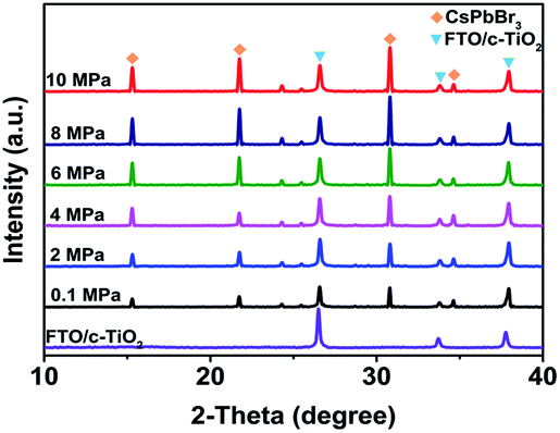 | ||
| Fig. 3 XRD patterns of the CsPbBr3 perovskite films prepared with different annealing pressures. | ||
The optical and photoelectric properties of the CsPbBr3 films were studied by UV-vis absorbance spectra and photoluminescence (PL) spectra. Fig. 4a showed the absorption spectra of the CsPbBr3 films. All the films possessed an absorption edge at ∼540 nm, which is characteristic of CsPbBr3 perovskite.3 As the annealing pressure increased, the absorbance of the films was enhanced, which can be explained by the better crystallinity and uniform grain size.23 From the Tauc plot (Fig. S3†) of (αhν)2 versus photon energy (hν), the bandgaps of CsPbBr3 films were calculated to be 2.35–2.36 eV by the Kubelka–Munk equation.13 As for the transmittance spectra at long wavelength region from 550 nm to 800 nm, the AP-10 film showed the highest transparency (Fig. 4b), indicating a dense and smooth morphology with lowest light scattering.
 | ||
| Fig. 4 (a) UV-vis absorption spectra and (b) transmittance spectra of the CsPbBr3 films with different annealing pressures; steady-state photoluminescence of the CsPbBr3 films deposited on substrate (c) with and (d) without electron transport layer. The inset of (c and d) are the corresponding time-resolved photoluminescence spectra of AP-0.1 and AP-10 sample. | ||
Steady-state PL and time-resolved PL spectroscopy were used to investigate the non-radiative recombination process in the CsPbBr3 films. As presented in Fig. 4c, without the electron transport layer (ETL), the intensity of the peaks at ∼540 nm increased significantly as the increasing of annealing pressure. The enhanced PL intensity can be attributed to the improved crystallinity of the film with large grains size. The corresponding TRPL decay curves of the AP-0.1 and AP-10 films were presented in Fig. 4c (insert). By using bi-exponential decay function,28 the curves were fitted to determine the decay times of the fast (τ1) and slow (τ2) components and the results were listed in Table S2.† The AP-0.1 and AP-10 films exhibited average carrier lifetimes (τavg) of 3.35 and 8.99 ns, respectively. In general, the longer carrier lifetime always coincided with a slower carrier recombination rate, inducing by low trap-state density in the films. For further understanding the intrinsic recombination behaviour of the solar devices, we studied the relationship between Voc and various incident light intensities (Ilight) of the devices. Generally, the function of Voc and Ilight can be described and fitted via the following formula:36 Voc ∝ nkT![[thin space (1/6-em)]](https://www.rsc.org/images/entities/char_2009.gif) ln(Ilight)/q, where n represent factors relate to bimolecular and trap-assisted recombination, k represents Boltzmann constant, T is absolute temperature in kelvin, q is an elementary charge. As shown in Fig. S4,† the n value of AP-10 device (1.73) is much smaller than that of the AP-0.1 device, suggesting lower trap-assisted recombination in the device.
ln(Ilight)/q, where n represent factors relate to bimolecular and trap-assisted recombination, k represents Boltzmann constant, T is absolute temperature in kelvin, q is an elementary charge. As shown in Fig. S4,† the n value of AP-10 device (1.73) is much smaller than that of the AP-0.1 device, suggesting lower trap-assisted recombination in the device.
In addition, we also performed the steady-state PL measurement on the CsPbBr3 films with FTO/compact-TiO2 substrates. As shown in Fig. 4d, the AP-10 sample exhibited a dramatically high degree of PL quenching in comparison with the AP-0.1 sample. Generally, this PL quenching is attributed to the efficient electron extraction across the perovskite/TiO2 interface. The charge lifetime obtained from TRPL decay curves (insert of Fig. 4d) further confirmed that the charge carrier extraction at the CsPbBr3/TiO2 interface could be enhanced by the annealing pressure.
To further verify the enhancement of crystal quality of CsPbBr3 films by high pressure annealing. All-inorganic PSCs with FTO/compact-TiO2/CsPbBr3/carbon architecture (Fig. 5a) were fabricated based on the as-prepared CsPbBr3 films. 60 devices were divided into 6 batches and each batch consists of 10 cells with the same annealing pressure. The current–voltage (J–V) performances of the devices were measured under one sun illumination (AM 1.5G). The distribution diagram of photovoltaic parameters (short-circuit current density (Jsc), open-circuit voltage (Voc), fill factor (FF) and power conversion efficiency (PCE)) were summarized in Fig. 5b. Clearly, with the increase of annealing pressure, all the J–V parameters improved significantly. The best device based on PA-0.1 films displayed a Jsc of 3.69 mA cm−2, a Voc of 1.26 V, a FF of 0.60, rendering a poor PCE of 2.79%. However, with the AP-10 films, the champion device achieved a Jsc of 6.49 mA cm−2, a Voc of 1.42 V, a FF of 0.79, with an overall PCE of 7.22% (Fig. 5c). The enhancement of photocurrent was checked by the photon-to-electron conversion efficiency (IPCE) measurement. As shown in Fig. 5d, the champion device exhibited a high IPCE value of ∼80% over the whole wavelength range of 450–525 nm. The integrated Jsc reached 6.43 mA cm−2, which is coincidence with the J–V result. Moreover, the long-term stability of the champion device was tested under 100 °C & RH = 80% condition without encapsulation. As shown in Fig. 5e, the device maintained 80% of its initial PCE over 30 days, showing excellent moisture and heat tolerance.
 | ||
| Fig. 5 (a) Device structure of CsPbBr3 PSCs; (b) the distribution diagram of photovoltaic parameters of CsPbBr3 PSCs with different annealing pressures; (c) J–V curves and (d) IPCE of the champion device; (e) long-term stability of the device under condition of 100 °C with 80% humidity. | ||
Conclusions
In summary, we developed a novel pressure-assisted annealing method for the preparation of high quality CsPbBr3 films. At standard atmospheric pressure (0.1 MPa), the CsPbBr3 film annealed at 335 °C exhibited poor crystallinity and high surface roughness with many pinholes. However, when we increased the pressure up to 10 MPa, the resulting CsPbBr3 film displayed a dense and smooth morphology with large average grain sizes over 1.5 µm. Further PL measurements revealed that the trap-state density in CsPbBr3 film can be dramatically decreased by the pressure. To identify the positive effect of annealing pressure on the optoelectronic performance of the CsPbBr3 film, we fabricated PSCs based on CsPbBr3 films annealed at different pressure. As a result, the device with the CsPbBr3 film annealed at 10 MPa showed a champion PCE of 7.22%, which was much higher than that with the film annealed at 0.1 MPa. We believe that this pressure-assisted annealing method could open a new path for achieving high-quality evaporated CsPbBr3 films.Conflicts of interest
There are no conflicts to declare.Acknowledgements
The authors acknowledge the financial support by National Natural Science Foundation of China (NSFC 51702243, 51972251, 91963209), the National Key Research and Development Program of China (No. 2018YFB1500104) and the Fundamental Research Funds for the Central Universities (WUT: 2016IVA093, 2017III022, 2018IVB031).Notes and references
- G. Xing, N. Mathews, S. Sun, S. S. Lim, Y. M. Lam, M. Gratzel, S. Mhaisalkar and T. C. Sum, Science, 2013, 342, 344–347 CrossRef PubMed.
- S. D. Stranks, G. E. Eperon, G. Grancini, C. Menelaou, M. J. Alcocer, T. Leijtens, L. M. Herz, A. Petrozza and H. J. Snaith, Science, 2013, 342, 341–344 CrossRef CAS PubMed.
- M. I. Saidaminov, A. L. Abdelhady, B. Murali, E. Alarousu, V. M. Burlakov, W. Peng, I. Dursun, L. Wang, Y. He, G. Maculan, A. Goriely, T. Wu, O. F. Mohammed and O. M. Bakr, Nat. Commun., 2015, 6, 1–6 Search PubMed.
- N. R. E. L. N. Best Research Cell_Efficiencies, 2019, https://www.nrel.gov/pv/cell-efficiency.html Search PubMed.
- E. J. Juarez-Perez, Z. Hawash, S. R. Raga, L. K. Ono and Y. Qi, Energy Environ. Sci., 2016, 9, 3406–3410 RSC.
- A. Dualeh, P. Gao, S. I. Seok, M. K. Nazeeruddin and M. Grätzel, Chem. Mater., 2014, 26, 6160–6164 CrossRef CAS.
- W. Tress, M. Yavari, K. Domanski, P. Yadav, B. Niesen, J. P. Correa Baena, A. Hagfeldt and M. Graetzel, Energy Environ. Sci., 2018, 11, 151–165 RSC.
- O. R. Yamilova, A. V. Danilov, M. Mangrulkar, Y. S. Fedotov, S. Y. Luchkin, S. D. Babenko, S. I. Bredikhin, S. M. Aldoshin, K. J. Stevenson and P. A. Troshin, J. Phys. Chem. Lett., 2019, 221–228, DOI:10.1021/acs.jpclett.9b03161.
- R. K. Misra, S. Aharon, B. Li, D. Mogilyansky, I. Visoly-Fisher, L. Etgar and E. A. Katz, J. Phys. Chem. Lett., 2015, 6, 326–330 CrossRef CAS PubMed.
- S. Chen, X. Du, D. Lin, F. Xie, W. Xie, L. Gong, W. Zhang, P. Liu and J. Chen, J. Electron Spectrosc. Relat. Phenom., 2018, 229, 108–113 CrossRef CAS.
- Q.-M. Hong, R.-P. Xu, T.-Y. Jin, J.-X. Tang and Y.-Q. Li, Org. Electron., 2019, 67, 19–25 CrossRef CAS.
- G. E. Eperon, G. M. Paternò, R. J. Sutton, A. Zampetti, A. A. Haghighirad, F. Cacialli and H. J. Snaith, J. Mater. Chem. A, 2015, 3, 19688–19695 RSC.
- M. Kulbak, D. Cahen and G. Hodes, J. Phys. Chem. Lett., 2015, 6, 2452–2456 CrossRef CAS.
- J. Duan, H. Xu, W. E. I. Sha, Y. Zhao, Y. Wang, X. Yang and Q. Tang, J. Mater. Chem. A, 2019, 7, 21036–21068 RSC.
- Y. Wang, X. Liu, T. Zhang, X. Wang, M. Kan, J. Shi and Y. Zhao, Angew. Chem., Int. Ed., 2019, 58, 16691–16696 CrossRef CAS.
- S. Dastidar, C. J. Hawley, A. D. Dillon, A. D. Gutierrez-Perez, J. E. Spanier and A. T. Fafarman, J. Phys. Chem. Lett., 2017, 8, 1278–1282 CrossRef CAS.
- A. Swarnkar, A. R. Marshall, E. M. Sanehira, B. D. Chernomordik, D. T. Moore, J. A. Christians, T. Chakrabarti and J. M. Luther, Science, 2016, 354, 92–95 CrossRef CAS.
- A. K. Jena, A. Kulkarni, Y. Sanehira, M. Ikegami and T. Miyasaka, Chem. Mater., 2018, 30, 6668–6674 CrossRef CAS.
- Y. Fu, M. T. Rea, J. Chen, D. J. Morrow, M. P. Hautzinger, Y. Zhao, D. Pan, L. H. Manger, J. C. Wright, R. H. Goldsmith and S. Jin, Chem. Mater., 2017, 29, 8385–8394 CrossRef CAS.
- H. L. Wells, Z. Anorg. Chem., 1893, 3, 195–210 CrossRef.
- J. Liang, C. X. Wang, Y. R. Wang, Z. R. Xu, Z. P. Lu, Y. Ma, H. F. Zhu, Y. Hu, C. C. Xiao, X. Yi, G. Y. Zhu, H. L. Lv, L. B. Ma, T. Chen, Z. X. Tie, Z. Jin and J. Liu, J. Am. Chem. Soc., 2016, 138, 15829–15832 CrossRef CAS PubMed.
- C. C. Stoumpos, C. D. Malliakas, J. A. Peters, Z. Liu, M. Sebastian, J. Im, T. C. Chasapis, A. C. Wibowo, D. Y. Chung, A. J. Freeman, B. W. Wessels and M. G. Kanatzidis, Cryst. Growth Des., 2013, 13, 2722–2727 CrossRef CAS.
- G. Tong, T. Chen, H. Li, L. Qiu, Z. Liu, Y. Dang, W. Song, L. K. Ono, Y. Jiang and Y. Qi, Nano Energy, 2019, 65, 104015 CrossRef CAS.
- Y. Zhao, J. Duan, Y. Wang, X. Yang and Q. Tang, Nano Energy, 2019, 104286, DOI:10.1016/j.nanoen.2019.104286.
- W. Chen, J. Zhang, G. Xu, R. Xue, Y. Li, Y. Zhou, J. Hou and Y. Li, Adv. Mater., 2018, 30, 1800855 CrossRef.
- J. Zhang, G. Hodes, Z. Jin and S. Liu, Angew. Chem., Int. Ed., 2019, 58, 15596–15618 CrossRef CAS.
- J. Duan, Y. Zhao, X. Yang, Y. Wang, B. He and Q. Tang, Adv. Energy Mater., 2018, 8, 1802346 CrossRef.
- J. Lei, F. Gao, H. Wang, J. Li, J. Jiang, X. Wu, R. Gao, Z. Yang and S. Liu, Sol. Energy Mater. Sol. Cells, 2018, 187, 1–8 CrossRef.
- X. Liu, X. Tan, Z. Liu, B. Sun, J. Li, S. Xi, T. Shi and G. Liao, J. Power Sources, 2019, 443, 227269 CrossRef.
- Y. El Ajjouri, F. Palazon, M. Sessolo and H. J. Bolink, Chem. Mater., 2018, 30, 7423–7427 CrossRef.
- W. Chen, J. Zhang, G. Xu, R. Xue, Y. Li, Y. Zhou, J. Hou and Y. Li, Adv. Mater., 2018, 30, e1800855 CrossRef.
- H. Li, G. Tong, T. Chen, H. Zhu, G. Li, Y. Chang, L. Wang and Y. Jiang, J. Mater. Chem. A, 2018, 6, 14255–14261 RSC.
- Y. Zhang, L. Luo, J. Hua, C. Wang, F. Huang, J. Zhong, Y. Peng, Z. Ku and Y.-b. Cheng, Mater. Sci. Semicond. Process., 2019, 98, 39–43 CrossRef CAS.
- T. Xiang, Y. Zhang, H. Wu, J. Li, L. Yang, K. Wang, J. Xia, Z. Deng, J. Xiao, W. Li, Z. Ku, F. Huang, J. Zhong, Y. Peng and Y.-B. Cheng, Sol. Energy Mater. Sol. Cells, 2019, 110317, DOI:10.1016/j.solmat.2019.110317.
- J. Xiao, Y. Yang, X. Xu, J. Shi, L. Zhu, S. Lv, H. Wu, Y. Luo, D. Li and Q. Meng, J. Mater. Chem. A, 2015, 3, 5289–5293 RSC.
- M. J. Speirs, D. N. Dirin, M. Abdu-Aguye, D. M. Balazs, M. V. Kovalenko and M. A. Loi, Energy Environ. Sci., 2016, 9, 2916–2924 RSC.
Footnote |
| † Electronic supplementary information (ESI) available. See DOI: 10.1039/d0ra00446d |
| This journal is © The Royal Society of Chemistry 2020 |