
 Open Access Article
 This Open Access Article is licensed under a
 Creative Commons Attribution 3.0 Unported Licence
Facile and efficient preparation of high-quality black phosphorus quantum dot films for sensing applications
Yan Zhao*ab,
Jie Huangab,
Ran Zhang ab,
Yinzhou Yanab and
Yongzhe Zhangc
ab,
Yinzhou Yanab and
Yongzhe Zhangc
aBeijing Engineering Research Center of Laser Technology, Institute of Laser Engineering, Beijing University of Technology, Beijing 100124, China. E-mail: zhaoyan@bjut.edu.cn
bKey Laboratory of Trans-scale Laser Manufacturing Technology, Ministry of Education, Institute of Laser Engineering, Beijing University of Technology, Beijing 100124, China
cCollege of Materials Science and Engineering, Beijing University of Technology, Beijing 100124, China
First published on 1st April 2020
Abstract
In this study, black phosphorus quantum dots (BPQDs) are synthesized by improved ultrasonic-assisted liquid exfoliation. The as-prepared BPQDs are deposited on large-area conductive substrates by electrophoretic deposition, and exhibit high-sensitivity humidity sensing and excellent electrical properties. The results offer not only a facile and efficient method to synthesise stable BPQDs films, but also a new opportunity to develop humidity sensors and nano-electronic devices.
1. Introduction
In the past decade, layered two-dimensional (2D) materials such as graphene, hexagonal boron nitride, and transition-metal dichalcogenides (TMDs) have attracted considerable attention because of their formidable physical and structural properties.1 Recently, atomically thin black phosphorus (BP) nanosheets have been successfully exfoliated from bulk BP crystals and fabricated into field-effect transistors (FETs).2 Thus far, BP has attracted considerable attention with respect to its physical, chemical, and biological properties. In contrast to graphene, BP is a 2D semiconductor with a sufficiently large tunable band gap,3 high carrier mobility,4 and remarkable in-plane anisotropic properties.5 These properties make BP a promising candidate for various applications, including optoelectronic devices,6–8 energy storage,9–11 gas sensors,12,13 and thermoelectric applications.14Numerous bottom-up synthesis methods, such as chemical vapor deposition using metallic catalysts,15–19 an epitaxial process,20–22 hydrothermal methods,23 and reduction methods,24,25 have been reported for 2D materials, even for ternary or heterostructure growth.26–32 These methods require complex, expensive equipment and harsh conditions without exceptions. Unfortunately, the synthesis of atomic-scale BP has not been adequately investigated because of its complicated chemistry as well as the instability of phosphorus. Efforts combining materials science and chemistry expertise should be devoted to the development of large-scale synthesis methods for BP thin films at the wafer scale, which can lead to additional applications, such as for other 2D materials such as graphene.33 Furthermore, it is also necessary to develop methods for the synthesis of large-area, high-quality thin films where the anisotropic properties of BP can be explored on a large scale.34 Recently, Li et al. have reported thin-film BP with a thickness of 40 nm on a flexible substrate by the deposition of a red phosphorus thin film on a flexible polyester substrate, followed by its conversion into BP using a high-pressure multi-anvil cell at room temperature.35 In addition, an amorphous BP film was successfully grown on Si/SiO2 or graphene/Cu substrates by pulsed laser deposition using a BP crystal as the precursor,36 affording poorly crystallized films with a thickness ranging from several nanometers to tens of nanometers.
Meanwhile, humidity sensors are attracting considerable attention in industrial and environmental fields. 2D materials such as graphene and TMDs have been widely examined for humidity sensing applications because of their high surface-to-volume ratios and excellent mechanical properties.37–41 Previously reported studies on BP demonstrate the ambient instability of the devices fabricated by atomically thin flakes;42–45 hence, micron-scale BP films have attracted considerable interest in the field of humidity sensors.46,47 However, the conventional method for preparing BP films requires high temperature and pressure,48,49 the film will be uneven,50–52 otherwise, the sensitivity performance of two-dimensional nanomaterial film humidity sensor needs to be improved.53,54
In this study, compared to traditional methods, electrophoretic deposition (EPD) was employed to synthesize high-quality BP quantum dot (BPQD) thin films at room temperature and atmospheric pressure. This simple method exhibits advantages of easy operation, cost-effectiveness, environmentally friendly nature, without the use of harsh conditions such as vacuum or inert atmosphere and high temperature and pressure. These BPQD film shows higher sensitivity in humidity detection than other thin film sensors. Impedance spectroscopy and electrical characterization revealed that the sensing mechanism of the BP film sensors is based on modulation of the leakage ionic current.
2. Results and discussion
Simple liquid exfoliation was utilized to prepare a highly dispersed suspension of ultra-small BPQDs with a lateral size of ∼10 nm. First, 30 mg of BP powder, which was weighed using an electronic balance, was dispersed into 100 mL of an isopropanol (IPA) solution cooled to 4° in a refrigerator, followed by ultrasonication (40 kHz) for 2 h in an ice water bath. Meanwhile, an ice block was added every 30 min, and the container was overturned every 1 min to completely exfoliate the BP powder and make a uniform, stable dispersion. The as-prepared BPQDs–IPA was stored in a sealed container. Fig. 1(a–c) shows the transmission electron microscopy (TEM) images of BPQDs. Statistical analysis based on TEM measurements was carried out to calculate the precise average diameter of BPQD samples: the QDs exhibited different diameters, with the predominant diameters ranging from 2.82 to ∼10 nm. The interlayer distance of BPQDs was statistically 0.235 nm. Uniform, stable BPQDs were synthesized by ultrasonic-assisted liquid exfoliation in an ice bath. Temperature and ultrasonic waves are well known to inhibit the agglomeration of BPQDs. In addition, uniform, small QDs lead to flat, smooth films. Furthermore, as shown in the high-resolution TEM image at a scale bar of 20 nm (Fig. 1a), a dense, disordered morphology without a long-range order was apparently observed at the interface between the grown film and substrate. This result indicated that BPQDs exhibit an ordered structure with an observed layered structure. Moreover, the selected-area electron diffraction (SAED) image showed a lattice pattern (Fig. 1d). These results further indicated that the obtained BPQDs exhibit perfect lattice structures.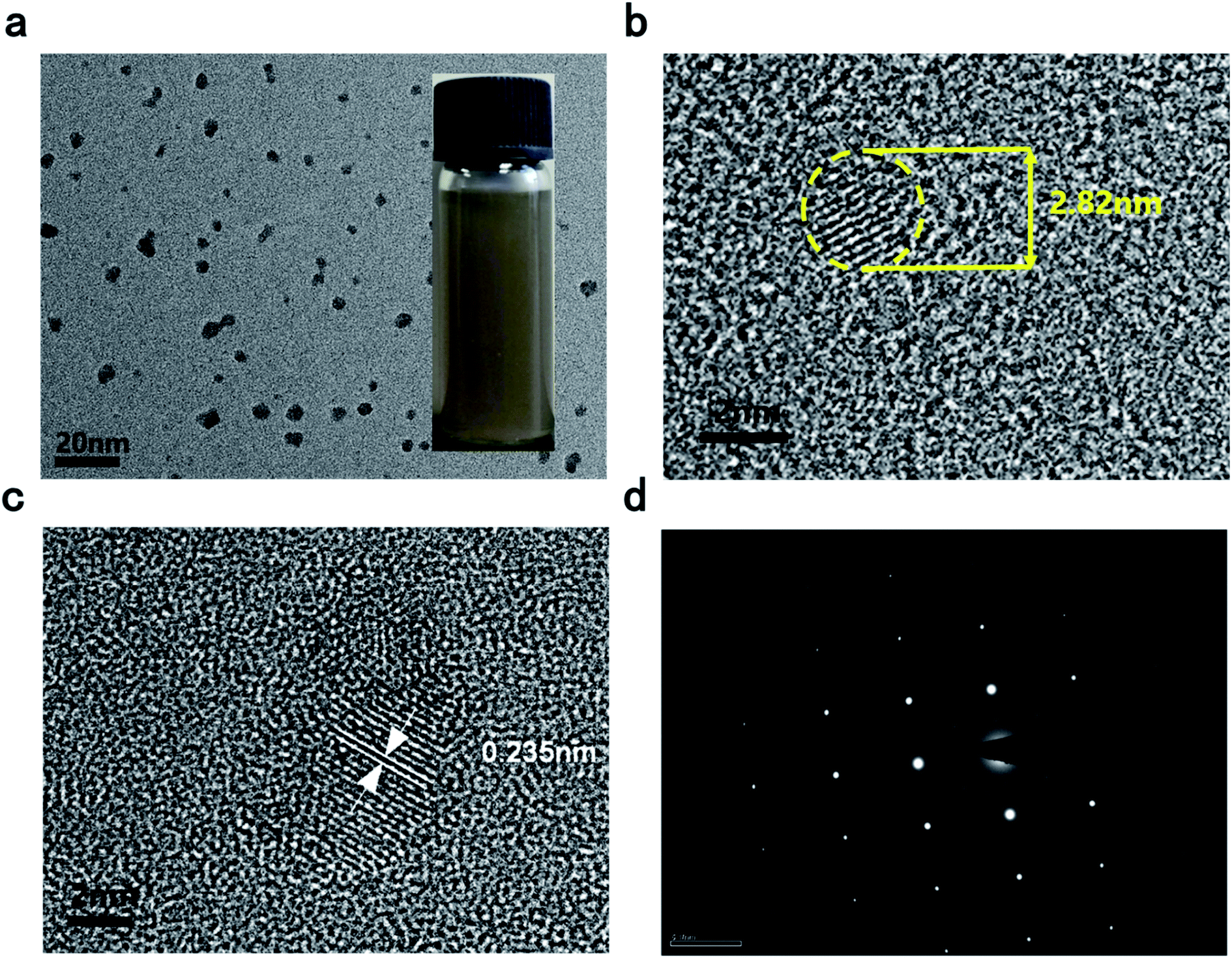 | ||
| Fig. 1 (a) TEM image (inset is the photograph of as-prepared BPDQs) (b and c) HR-TEM image (d) the selected-area electron diffraction (SAED) pattern of BPQDs. | ||
BPQDs were deposited on a silicon substrate by EPD. BPQDs with diameters ranging from 3 to 10 nm, which were prepared by liquid exfoliation, were used. Mixtures of magnesium nitrate (Mg(NO3)2) and IPA at different volume ratios were used as the suspension solvent, and 0.2 mg mL−1 of BPQDs was dispersed into the solvent, after ultrasonication for 30 min, affording a stable suspension. The cathode and anode were connected to a silicon wafer and graphite electrode, respectively. The two electrodes were maintained parallel to each other at a distance of 30 mm in the suspension, and a constant deposition voltage of 110 V was used for EPD. X-ray diffraction (XRD) and TEM were utilized to examine the structural properties of BPQD films: a perfect crystal structure and clearly identified phases were observed for the BPQD films (Fig. 2b). Fig. 2c shows the Raman spectra of BPQDs films: A1g (out-of-plane), B2g, and A2g (in-plane) Raman peaks were observed at 362, 438, and 467 cm−1, respectively, for BPQD films prepared by EPD. For bulk samples, Raman peaks corresponding to the A1g, B2g, and A2g modes were observed at 363, 437, and 468 cm−1, respectively. An extremely similar distribution of the peak positions between the films and bulk was observed,55 indicative of the good crystalline quality of the sample after EPD. Meanwhile, thin films of different thicknesses, i.e., ranging from 0.3 to 5 μm, were also prepared by adjusting the parameters. The thickness of films was measured by the optical profiler of WykoNT1100 (Veeco). We can see that the Raman peak of the black phosphorus quantum dot film is wider than the bulk black phosphorus, because the black phosphorus quantum dot film has a different structure from the bulk black phosphorus. The bulk black phosphorus lattice structure is single and stable, with a fixed bond angle and bond length. Therefore, the position of its Raman characteristic peak is determined. Black phosphorus quantum dots are formed in clusters. There is mechanical strain between black phosphorus clusters of different sizes. As the thickness of the black phosphorus quantum dot film increases, small black phosphorus quantum dot clusters will gradually for large-scale transitions. Different sizes of black phosphorus quantum dots exhibit different mechanical strain, thereby changing the bond length and bond angle of their physical structure to a small extent, making them show a small difference in Raman peak positions. Raman peaks become wider due to the coexistence of black phosphorus quantum dot clusters of different sizes. With increasing thickness, the peak intensity relatively increased. The BPQD–IPA concentration played a major role in the film thickness, in addition to deposition time and voltage. Moreover, the scale of the films can be regulated and controlled by changing the electrode size. In contrast to the conventional method, the method developed herein can be used for the facile control of the thickness and scale of the films at room temperature and atmospheric pressure.48,49
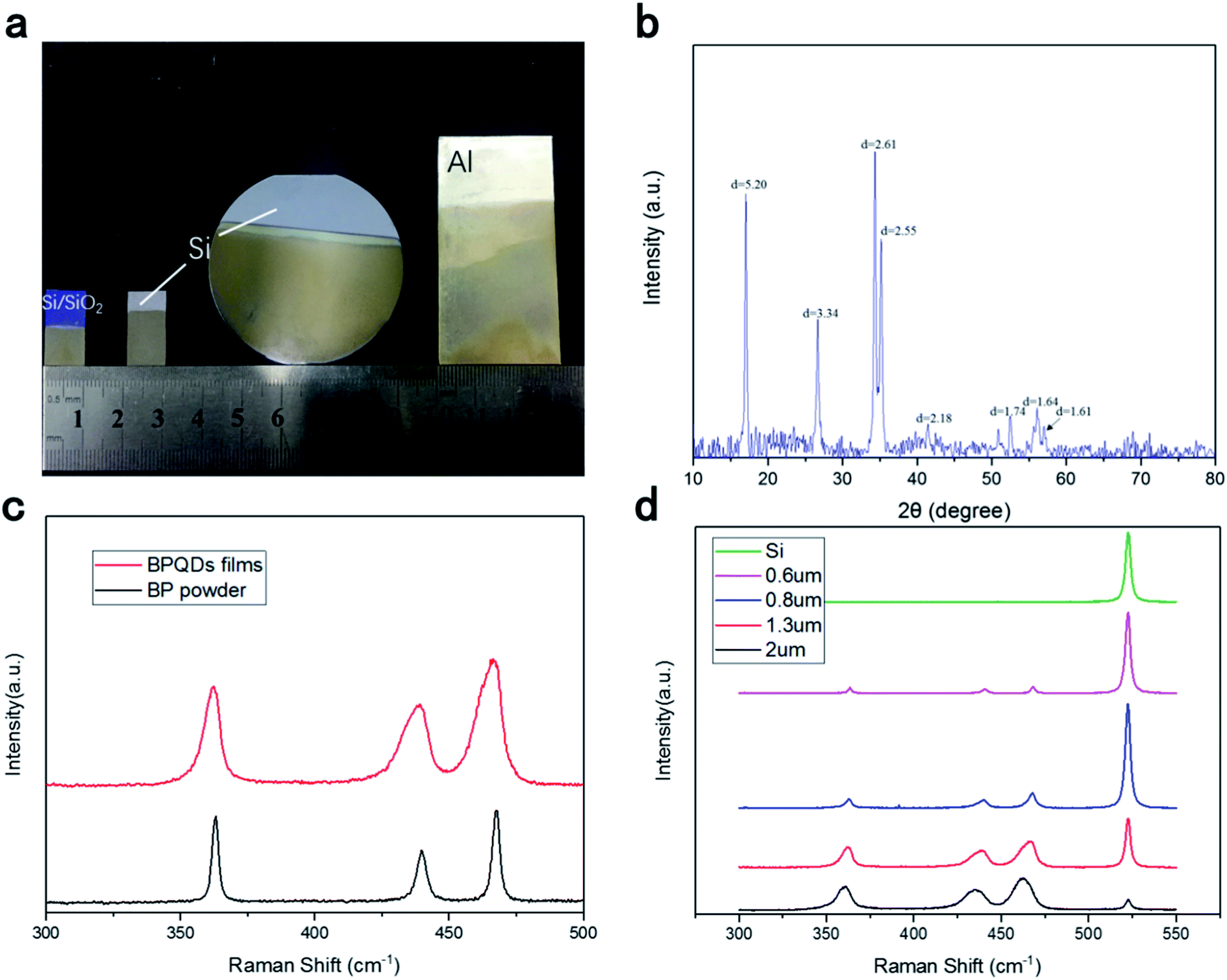 | ||
| Fig. 2 (a) Photographs of samples prepared by electrophoretic deposition on different substrates (from left to right: Si/SiO2, Si, Al). (b) XRD results of BPQD films. (c) Raman spectra of 800 nm-thick BPQD films and of BP powder. (d) Raman spectra of the BPQD films with different thicknesses and Si substrate. | ||
Clearly, the film surface prepared by drop-coating was not smooth because of the coffee-ring effect (Fig. 3a). A flat, smooth cross-section profile for the BPQD films was observed (Fig. 3(b)). This method leads to significant improvement in the film surface smoothness and the decrease in the dynamic friction coefficient. This feature revealed the long-term stability of the BPQD films used in optoelectronic devices. This system improves the measurement precision via the average of the testing values from repeated measurements. The roughness of the BPQDs prepared by EPD (Ra = 0.06 um) was superior to that prepared by the drop-coating method (Ra = 0.23 um, Fig. 3(c)).
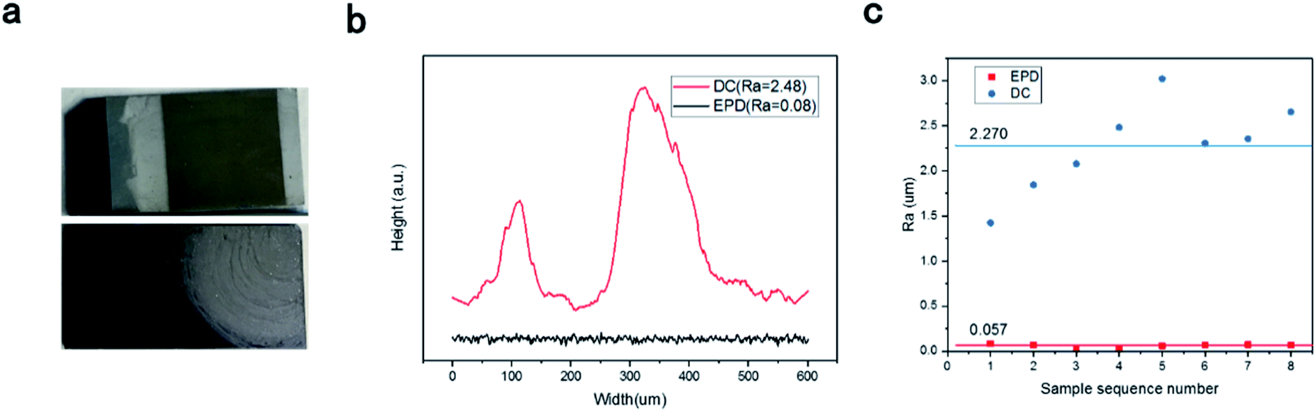 | ||
| Fig. 3 (a) Photographs of samples prepared by electrophoretic deposition (EPD, top) and the drop-coating method (DC, bottom). (b) Cross-section profile and (c) arithmetic mean deviation of surface roughness (Ra) of the BPQD films prepared by EPD and DC. | ||
After a series of confirmatory experiments, the mechanism for the synthesis of BPQD films by EPD is thought to occur by the following four processes (Fig. 2): (1) Polarization: magnesium nitrate (Mg(NO3)2) ionizes in the IPA solution, affording free magnesium ions (Mg2+). In the BP structure, one phosphorus with five valence electrons provides three electrons for a covalent bond with the other three. Hence, two outermost electrons are free. BPQDs easily adsorb Mg2+ because of its high surface area, affording coordinate covalent bonds with Mg2+ (Fig. 4). [BP Mg]2+ polarizes under an electric field. (2) Mobility: under an electric field, positively charged particles in a colloid shift to the cathode, while negative particles shift to the anode. Therefore, [BP Mg]2+ shifts to the cathode. (3) Adsorption: similar to the repulsion of electric charges, unlike charges attract each other. [BP Mg]2+ groups are adsorbed on the cathode surface. (4) Separation: as a result of charge transfer, BP groups undergo depolarization after their contact with the cathode, which are separated from Mg2+. At length, BPQDs were deposited on the Si/SiO2 substrate.
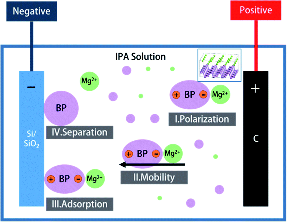 | ||
| Fig. 4 Mechanism for the synthesis of BPQD films by electrophoretic deposition. | ||
Fig. 4(a) shows the structure of the BPQD-film humidity sensor. The silicon substrate was modified with thin aluminum interdigital electrodes by utilizing vacuum evaporate plating technology. This structure leads to the increased sensitivity of the BPQD film humidity sensor because that more influences of interface state were introduced due to the interdigital electrode configuration. The distance between the electrodes was 0.5 mm. Interdigital electrodes separated by a small distance can lead to the decreased modulation voltage and effectively improved tunability. Fig. 4(b) shows the current–voltage (I–V) characteristics of the BPQD film sensor: With increasing humidity from 20% to 90%, the I–V incline increased. Fig. 4(c) shows a series of sensing resistance data as a function of the relative humidity (RH) at room temperature. Specifically, with the increase in RH from 20% to 90%, the resistance of the sensor decreased by ∼4 orders of magnitude. BPQDs with a high specific surface area will easily adsorb water molecules from air, leading to autoionization on the BPQD film surface, and the dissociation of the hydrogen–oxygen bond, affording protons (H+) from water molecules, and formed hydroxide ion (OH−). This released proton combines with another water molecule to form a hydrated cation (H3O+). In a low-humidity environment (20%), a small amount of water molecules can adhere to the BPQD film surface, implying the formation of a small amount of H3O+ and a lower electrical conductivity for the BPQD films. On the other hand, at a higher humidity of 90%, the films exhibited higher electrical conductivity, related to the presence of a high amount of H3O+.
The calculation formula for the humidity sensitivity of the black phosphorus quantum dot film humidity sensor is as follows:
The sensitivity in the formula is defined as the ratio of the change in resistance to the change in relative humidity. The sensitivity value in this paper is calculated to be approximately equal to 1150.
3. Conclusions
In conclusion, BPQDs with a lateral size of ∼10 nm was prepared by simple liquid exfoliation. Furthermore, high-sensitivity, stable humidity detection was investigated using the BPQD thin films prepared by electrophoretic deposition. In contrast to the conventional method, the method developed herein can lead to the facile control of the thickness and scale of the films at room temperature and atmospheric pressure. This flat BPQD film with long-term stability demonstrates immense potential for optoelectronic devices, energy storage, gas sensors, and thermoelectric applications.4. Experimental section
Syntheses and characterization of BPQDs
A highly dispersed suspension of ultra-small BPQDs with a lateral size of ∼10 nm was prepared by simple liquid exfoliation. First, 30 mg of black phosphorus powder, which was weighed using an electronic balance, was dispersed in 100 mL of an isopropanol solution cooled to 4° in a refrigerator, followed by ultrasonication (40 kHz) for 2 h in an ice water bath. Next, an ice block was added every 30 min, the and the container was overturned after 1 min each to completely exfoliate the BP powder and make a stable, uniform dispersion. The as-prepared BPQD–IPA was stored in a sealed container.Deposition of BPQD films by electrophoretic deposition
BP quantum dots were deposited on the silicon substrate by electrophoretic deposition. BPQDs with diameters ranging from 3 to 10 nm, which were prepared by liquid exfoliation, were used. Mixtures of magnesium nitrate (Mg(NO3)2) and IPA with different volume ratios were used as the suspension solvent, and 0.2 mg mL−1 of BPQDs was dispersed into the solvent, after ultrasonication for 30 min, to form a stable suspension. The cathode and anode were connected to a silicon wafer and graphite electrode, respectively. The two electrodes were maintained parallel to each other at a distance of 30 mm in the suspension, and a constant deposition voltage of 110 V was used.Characterization of BPQDs and BPQDs films
The amorphous phase was characterized by X-ray diffraction (Rigaku Smartlab, Japan) with Cu Kα radiation (λ = 1.5406 Å). Transmission electron microscopy (JEOL JEM 2400, Japan) was employed to examine the detailed microstructures and chemical compositions. Cross-sectional TEM specimens were prepared by the application of FIB (JEOL JIB-4500) milling and a lift-off technique. The samples thus obtained were transferred on a copper grid for TEM characterization. The thickness of BPQD films and surface morphology were determined by atomic force microscopy (Park XE-100 AFM). Raman spectra were recorded on a Raman system (T64000 JHON YVORN) equipped with a 532 nm laser source.Fabrication and electrical measurements of the BPQD film humidity sensor
The silicon substrate was modified with thin aluminum interdigital electrodes by utilizing vacuum evaporate plating technology. This structure increases the sensitivity of the BPQD-film humidity sensor because that more influences of interface state were introduced due to the interdigital electrode configuration. The distance between the electrodes was 0.5 mm. Interdigital electrodes with a small distance can decrease the modulation voltage and effectively improve tunability (Fig. 5).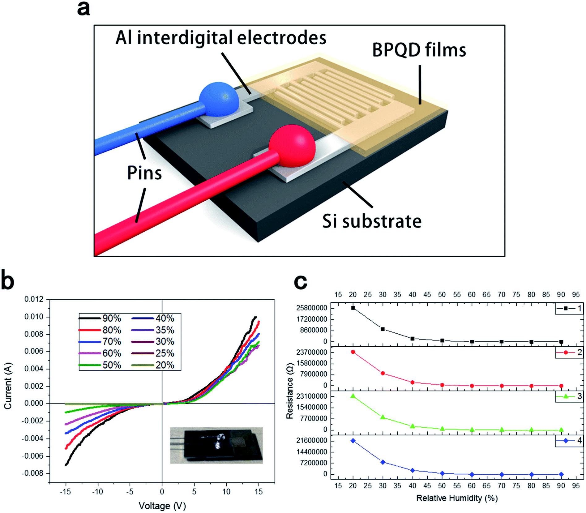 | ||
| Fig. 5 (a) Structure of the BPQD-film humidity sensor. (b) Current–voltage (I–V) characteristics of the BPQD-film humidity sensor. (c) Sensor resistance as a function of the relative humidity (RH) of the sensor after four tests. | ||
Conflicts of interest
There are no conflicts to declare.Acknowledgements
We acknowledge the National Natural Science Foundation of China (51475014) for the financial support.References
- A. J. Mannix, B. Kiraly, M. C. Hersam and N. P. Guisinger, Synthesis and chemistry of elemental 2D materials, Nat. Rev. Chem., 2017, 1, 0014 CrossRef CAS.
- L. Li, Y. Yu, G. J. Ye, Q. Ge, X. Ou, H. Wu, D. Feng, X. H. Chen and Y. Zhang, Black phosphorus field-effect transistors, Nat. Nanotechnol., 2014, 9, 372 CrossRef CAS PubMed.
- J. Kim, et al., Observation of tunable band gap and anisotropic Dirac semimetal state in black phosphorus, Science, 2015, 349(6249), 723–726 CrossRef CAS PubMed.
- J. Qiao, et al., High-mobility transport anisotropy and linear dichroism in few-layer black phosphorus, Nat. Commun., 2014, 5, 4475 CrossRef CAS PubMed.
- X. Wang, et al., Highly anisotropic and robust excitons in monolayer black phosphorus, Nat. Nanotechnol., 2015, 10(6), 517 CrossRef CAS PubMed.
- M. Engel, M. Steiner and P. Avouris, lack phosphorus photodetector for multispectral, high-resolution imaging, Nano Lett., 2014, 14(11), 6414–6417 CrossRef CAS PubMed.
- N. Youngblood, et al., Waveguide-integrated black phosphorus photodetector with high responsivity and low dark current, Nat. Photonics, 2015, 9(4), 247 CrossRef CAS.
- H. Yuan, et al., Polarization-sensitive broadband photodetector using a black phosphorus vertical p–n junction, Nat. Nanotechnol., 2015, 10(8), 707 CrossRef CAS PubMed.
- V. V. Kulish, et al., Phosphorene as an anode material for Na-ion batteries: a first-principles study, Phys. Chem. Chem. Phys., 2015, 17(21), 13921–13928 RSC.
- L. Wang, Z. Sofer and P. Martin, Voltammetry of Layered Black Phosphorus: Electrochemistry of Multilayer Phosphorene, ChemElectroChem, 2015, 2(3), 324–327 CrossRef CAS.
- J. Sun, et al., A phosphorene–graphene hybrid material as a high-capacity anode for sodium-ion batteries, Nat. Nanotechnol., 2015, 10(11), 980 CrossRef CAS PubMed.
- L. Kou, T. Frauenheim and C. Chen, Phosphorene as a superior gas sensor: selective adsorption and distinct I–V response, J. Phys. Chem. Lett., 2014, 5(15), 2675–2681 CrossRef CAS PubMed.
- S. Cui, et al., Ultrahigh sensitivity and layer-dependent sensing performance of phosphorene-based gas sensors, Nat. Commun., 2015, 6, 8632 CrossRef CAS PubMed.
- E. Flores, et al., Thermoelectric power of bulk black-phosphorus, Appl. Phys. Lett., 2015, 106(2), 022102 CrossRef.
- C. -an Di, et al., Patterned graphene as source/drain electrodes for bottom-contact organic field-effect transistors, Adv. Mater., 2008, 20(17), 3289–3293 CrossRef CAS.
- S. J. Chae, et al., Synthesis of large-area graphene layers on poly-nickel substrate by chemical vapor deposition: wrinkle formation, Adv. Mater., 2009, 21(22), 2328–2333 CrossRef CAS.
- Van L. Nguyen and H. L. Young, Towards Wafer-Scale Monocrystalline Graphene Growth and Characterization, Small, 2015, 11(29), 3512–3528 CrossRef CAS PubMed.
- D. Ma, et al., High-Quality Monolayer Graphene Synthesis on Pd Foils via the Suppression of Multilayer Growth at Grain Boundaries, Small, 2014, 10(19), 4003–4011 CrossRef CAS PubMed.
- Y. Xue, et al., Controllable synthesis of doped graphene and its applications, Small, 2014, 10(15), 2975–2991 CrossRef CAS PubMed.
- C. Berger, et al., Electronic confinement and coherence in patterned epitaxial graphene, Science, 2006, 312(5777), 1191–1196 CrossRef CAS PubMed.
- P. W. Sutter, J.-I. Flege and E. A. Sutter, Epitaxial graphene on ruthenium, Nat. Mater., 2008, 7(5), 406 CrossRef CAS PubMed.
- M. Liu, et al., Single and polycrystalline graphene on Rh (111) following different growth mechanisms, Small, 2013, 9(8), 1360–1366 CrossRef CAS PubMed.
- G. Huang, et al., Graphene-Like MoS2/Graphene Composites: Cationic Surfactant-Assisted Hydrothermal Synthesis and Electrochemical Reversible Storage of Lithium, Small, 2013, 9(21), 3693–3703 CrossRef CAS PubMed.
- S. Wu, et al., Electrochemically reduced single-layer MoS2 nanosheets: characterization, properties, and sensing applications, Small, 2012, 8(14), 2264–2270 CrossRef CAS PubMed.
- S. Stankovich, et al., Synthesis of graphene-based nanosheets via chemical reduction of exfoliated graphite oxide, Carbon, 2007, 45(7), 1558–1565 CrossRef CAS.
- Z. Liu, et al., Direct growth of graphene/hexagonal boron nitride stacked layers, Nano Lett., 2011, 11(5), 2032–2037 CrossRef CAS PubMed.
- Z. Liu, et al., In-plane heterostructures of graphene and hexagonal boron nitride with controlled domain sizes, Nat. Nanotechnol., 2013, 8(2), 119 CrossRef CAS PubMed.
- Q. Feng, et al., Growth of Large-Area 2D MoS2 (1-x) Se2x Semiconductor Alloys, Adv. Mater., 2014, 26(17), 2648–2653 CrossRef CAS PubMed.
- Y. Gong, et al., Vertical and in-plane heterostructures from WS2/MoS2 monolayers, Nat. Mater., 2014, 13(12), 1135 CrossRef CAS PubMed.
- X. Duan, et al., Lateral epitaxial growth of two-dimensional layered semiconductor heterojunctions, Nat. Nanotechnol., 2014, 9(12), 1024 CrossRef CAS PubMed.
- C. Huang, et al., Lateral heterojunctions within monolayer MoSe2–WSe2 semiconductors, Nat. Mater., 2014, 13(12), 1096 CrossRef CAS PubMed.
- M.-Y. Li, et al., Epitaxial growth of a monolayer WSe2-MoS2 lateral pn junction with an atomically sharp interface, Science, 2015, 349(6247), 524–528 CrossRef CAS PubMed.
- J.-H. Lee, et al., Wafer-scale growth of single-crystal monolayer graphene on reusable hydrogen-terminated germanium, Science, 2014, 344(6181), 286–289 CrossRef CAS PubMed.
- Xi Ling, et al., The renaissance of black phosphorus, Proc. Natl. Acad. Sci. U. S. A., 2015, 112(15), 4523–4530 CrossRef CAS PubMed.
- X. Li, B. Deng, X. Wang, S. Chen, M. Vaisman, S. Karato, G. Pan, M. Larry Lee, J. Cha, H. Wang and F. Xia, 2D Mater, 2015, 2, 031002 CrossRef.
- Z. Yang, et al., Field-Effect Transistors Based on Amorphous Black Phosphorus Ultrathin Films by Pulsed Laser Deposition, Adv. Mater., 2015, 27(25), 3748–3754 CrossRef CAS PubMed.
- S. Borini, et al., Ultrafast graphene oxide humidity sensors, ACS Nano, 2013, 7(12), 11166–11173 CrossRef CAS PubMed.
- Y. Yao, et al., Graphene oxide thin film coated quartz crystal microbalance for humidity detection, Appl. Surf. Sci., 2011, 257(17), 7778–7782 CrossRef CAS.
- J. Zhao, et al., Highly Sensitive MoS2 Humidity Sensors Array for Noncontact Sensation, Adv. Mater., 2017, 29, 34 Search PubMed.
- H. Bi, et al., Ultrahigh humidity sensitivity of graphene oxide, Sci. Rep., 2013, 3, 2714 CrossRef PubMed.
- S.-Ha Hwang, et al., Poly (vinyl alcohol) reinforced and toughened with poly (dopamine)-treated graphene oxide, and its use for humidity sensing, ACS Nano, 2014, 8(7), 6739–6747 CrossRef CAS PubMed.
- J. D. Wood, et al., Effective passivation of exfoliated black phosphorus transistors against ambient degradation, Nano Lett., 2014, 14(12), 6964–6970 CrossRef CAS PubMed.
- J. O. Island, et al., Environmental instability of few-layer black phosphorus, 2D Materials, 2015, 2(1), 011002 CrossRef.
- J. Kang, et al., Solvent exfoliation of electronic-grade, two-dimensional black phosphorus, ACS Nano, 2015, 9(4), 3596–3604 CrossRef CAS PubMed.
- A. Favron, et al., Photooxidation and quantum confinement effects in exfoliated black phosphorus, Nat. Mater., 2015, 14(8), 826 CrossRef CAS PubMed.
- P. Yasaei, et al., Stable and selective humidity sensing using stacked black phosphorus flakes, ACS Nano, 2015, 9(10), 9898–9905 CrossRef CAS PubMed.
- D. J. Late, Liquid exfoliation of black phosphorus nanosheets and its application as humidity sensor, Microporous Mesoporous Mater., 2016, 225, 494–503 CrossRef CAS.
- Q. Jiang, et al., Facile synthesis of black phosphorus: an efficient electrocatalyst for the oxygen evolving reaction, Angew. Chem., Int. Ed., 2016, 55(44), 13849–13853 CrossRef CAS PubMed.
- Z. Yang, et al., Field-Effect Transistors Based on Amorphous Black Phosphorus Ultrathin Films by Pulsed Laser Deposition, Adv. Mater., 2015, 27(25), 3748–3754 CrossRef CAS PubMed.
- D. Hanlon, et al., Liquid exfoliation of solvent-stabilized few-layer black phosphorus for applications beyond electronics, Nat. Commun., 2015, 6, 8563 CrossRef CAS PubMed.
- M. B. Erande, S. P. Mahendra and J. L. Dattatray, Humidity sensing and photodetection behavior of electrochemically exfoliated atomically thin-layered black phosphorus nanosheets, ACS Appl. Mater. Interfaces, 2016, 8(18), 11548–11556 CrossRef CAS PubMed.
- C. Zhu, et al., Ultrafast preparation of black phosphorus quantum dots for efficient humidity sensing, Chem.–Eur. J., 2016, 22(22), 7357–7362 CrossRef CAS PubMed.
- H. Bi, K. Yin and X. Xie, et al., Ultrahigh humidity sensitivity of graphene oxide, Sci. Rep., 2013, 3, 2714 CrossRef PubMed.
- A. N. Abbas, B. Liu and L. Chen, et al., Black phosphorus gas sensors, ACS Nano, 2015, 9(5), 5618–5624 CrossRef CAS PubMed.
- M. B. Erande, et al., Electrochemically exfoliated black phosphorus nanosheets–prospective field emitters, Eur. J. Inorg. Chem., 2015, 19(2015), 3102–3107 CrossRef.
| This journal is © The Royal Society of Chemistry 2020 |