
 Open Access Article
 This Open Access Article is licensed under a Creative Commons Attribution-Non Commercial 3.0 Unported Licence
Copper halide diselenium: predicted two-dimensional materials with ultrahigh anisotropic carrier mobilities†
Fazel Shojaeiab,
Maryam Azizi b,
Zabiollah Mahdavifar*a,
Busheng Wangc and
Gilles Frapper*c
b,
Zabiollah Mahdavifar*a,
Busheng Wangc and
Gilles Frapper*c
aDepartment of Chemistry, Faculty of Science, Shahid Chamran University of Ahvaz, Ahvaz, Iran. E-mail: z_mahdavifar@scu.ac.ir; Fax: +98-611-3331042
bSchool of Nanoscience, Institute for Research in Fundamental Sciences (IPM), P. O. Box: 19395-5531, Tehran, Iran
cIC2MP UMR 7285, Université de Poitiers – CNRS, 4, Rue Michel Brunet TSA 51106-86073, Cedex 9, Poitiers, France. E-mail: gilles.frapper@univ-poitiers.fr
First published on 24th February 2020
Abstract
On the basis of first-principles calculations, we discuss a new class of two-dimensional materials—CuXSe2 (X = Cl, Br) nanocomposite monolayers and bilayers—whose bulk parent was experimentally reported in 1969. We show the monolayers are dynamically, mechanically and thermodynamically stable and have very small cleavage energies of ∼0.26 J m−2, suggesting their exfoliation is experimentally feasible. The monolayers are indirect-gap semiconductors with practically the same moderate band gaps of 1.74 eV and possess extremely anisotropic and very high carrier mobilities (e.g., their electron mobilities are 21![[thin space (1/6-em)]](https://www.rsc.org/images/entities/char_2009.gif) 263.45 and 10274.83 cm2 V−1 s−1 along the Y direction for CuClSe2 and CuBrSe2, respectively, while hole mobilities reach 2054.21 and 892.61 cm2 V−1 s−1 along the X direction). CuXSe2 bilayers are also indirect band gap semiconductors with slightly smaller band gaps of 1.54 and 1.59 eV, suggesting weak interlayer quantum confinement effects. Moreover, the monolayers exhibit high absorption coefficients (>105 cm−1) over a wide range of the visible light spectra. Their moderate band gaps, very high unidirectional electron and hole mobilities, and pronounced absorption coefficients indicate the proposed CuXSe2 (X = Cl, Br) nanocomposite monolayers hold significant promise for application in optoelectronic devices.
263.45 and 10274.83 cm2 V−1 s−1 along the Y direction for CuClSe2 and CuBrSe2, respectively, while hole mobilities reach 2054.21 and 892.61 cm2 V−1 s−1 along the X direction). CuXSe2 bilayers are also indirect band gap semiconductors with slightly smaller band gaps of 1.54 and 1.59 eV, suggesting weak interlayer quantum confinement effects. Moreover, the monolayers exhibit high absorption coefficients (>105 cm−1) over a wide range of the visible light spectra. Their moderate band gaps, very high unidirectional electron and hole mobilities, and pronounced absorption coefficients indicate the proposed CuXSe2 (X = Cl, Br) nanocomposite monolayers hold significant promise for application in optoelectronic devices.
1. Introduction
Inspired by the discovery of graphene monolayers in 2004,1 scientists have undertaken extensive research efforts to explore other two-dimensional (2D) materials. Due to their broad range of unique physicochemical and electronic properties, 2D materials hold promise for several technological applications, such as nanoelectronics,2–4 catalysis5–7 and energy conversion/storage.8–10 Chemical composition is well-recognized to determine the electronic properties of 2D materials, i.e., graphene is a zero band gap material1 while phosphorene is a semiconductor with a band gap of approximately 1.45 eV.11 However, only a small number of 2D elemental compounds have actually been synthesized.12 Most 2D materials are binary (AxBy) and ternary (AxByCz) compounds that exhibit highly diverse structural and electronic properties. In the last few years, 2D ternary compounds have received considerable research attention because of the higher possibility of tuning their properties due to the multiple degrees-of-freedom in their chemical compositions. Metal phosphorus trichalcogenides (MPX3: MnPSe3, MnPS3, FePS3, etc),13 ternary MXenes14 and ternary transition metal dichalcogenides15 are typical 2D ternary compounds.Copper halogen dichalcogenides with the chemical formula CuXY2, where X = Cl, Br or I and Y = Se or Te, are an emerging class of ternary layered materials.16–20 Copper halide dichalcogens were first synthesized in 196916 and their crystal structures were identified in 1988.17 This class of materials is also called layered nanocomposites, as the chalcogen nanochains are inserted into the matrix of the CuX system. To the best of our knowledge—other than their experimental synthesis—there are very few reports on this class of material. However, the potential applications of CuClSe2, the first copper halide dichalcogen to be synthesized, have been experimentally investigated in optoelectronic devices.21,22 Previous studies showed the compound is a semiconductor with an indirect band gap of 1.45 eV and very high absorption coefficients in the range of 104–105 cm−1.21 Additionally, the low cost, convenient preparation, and high efficiency of CuClSe2 make it a promising light absorber material that could potentially be exploited in solar cells. Therefore, it is of great importance to understand the electronic and optical properties of this type of material.
In this work, we studied the stability and mechanical, electronic and optical properties of CuXSe2 (X = Cl, Br) monolayers using first-principles calculations. The monolayers are predicted to possess good dynamic, mechanical and thermodynamic stabilities. The CuXSe2 monolayers can be easily exfoliated from the bulk, indicating weak interlayer interactions. The monolayers are semiconductors with indirect band gaps of 1.73 eV for CuClSe2 and 1.74 for CuBrSe2. Remarkably, extremely anisotropic and very high mobilities of ∼104 cm2 V−1 s−1 for electrons and ∼103 cm2 V−1 s−1 for holes are observed for both materials, implying efficient separation of photo-generated electrons and holes. In addition, the monolayers show strong absorption over a wide range of the visible light spectrum, indicating their promising potential as light absorber materials.
2. Theoretical methods
The first-principles calculations use a plane-wave basis with an energy cutoff of 400 eV and the projector augmented wave (PAW)23 method as implemented in the Vienna Ab initio Simulation Package (VASP) code.24,25 For structure (shape, volume, and atomic positions) and energy determination, the Perdew–Burke–Ernzerhof (PBE) functional26 at the generalized gradient approximation (GGA)26 level of theory was used, if not otherwise noted. We investigated the performance for structural parameters and cleavage energy for a selective set of vdW DFT methods (optB88, SCAN-rVV10, DFT-dDsC, FIA and PBE-D2, using standard production settings in VASP code) in modelling non-covalent vdW interactions in layered bulk CuXSe2 (X = Cl, Br) structures. Calculated structural parameters and cleavage energies are tabulated in Table S1 in ESI.† Considering both accuracy and computationally efficiency, Grimme's D2 correction (PBE-D2)27 is selected for this work. For the 2D systems, we set a sufficiently large vacuum space to avoid interactions between neighboring images. K-point sampling was performed using Γ-centered 10 × 8 × 6 and 10 × 8 × 1 for bulk and 2D systems, respectively. All of the structures were fully optimized until the net forces on atoms were below 1 meV Å−1, resulting in enthalpies that converged to better than 1 meV per atom. Since PBE is known to systematically underestimate the band gap for semiconductors, the Heyd–Scuseria–Ernzerhof hybrid functional (HSE06) was employed for high-accuracy electronic structure calculations.28In order to evaluate the dynamic stability of the monolayers, phonon dispersion relations were calculated by employing density functional perturbation theory (DFPT), as implemented in the Phonopy package,29,30 using VASP as the force-constant calculator. To further verify the thermal stability of the monolayers, Nose–Hoover ab initio molecular dynamics (AIMD) simulations were performed for constant NVT systems with a time step of 1.0 fs and Γ-point sampling (see Computational details in S2, ESI†).31–33
In a 2D system, carrier mobility34 can be calculated from the deformation potential approximation:
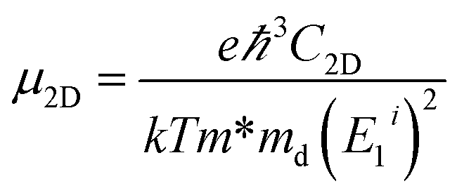 | (1) |
 and E1i mimics the deformation energy constant of the carrier due to phonons for the i-th edge band along the transport direction through the relation E1i = ΔEi/(Δl/l0), where ΔEi and Δl/l0 represent the energy change of the i-th band and lattice dilation, respectively.
To perform chemical bonding analysis, we carried out single-point calculations (using the geometries obtained from VASP) to calculate the density of states (DOS), crystal overlap Hamilton population (COHP) using the LOBSTER package,35 and electron localization function (ELF). Molecular orbital diagrams were generated via the extended Hückel method36 using CACAO code.37 Images of the crystalline structures reported in ESI (S3 and S4†) and crystal orbitals were produced using VESTA software package.38
3. Results and discussion
Here, we take CuClSe2 as a representative bulk example of isostructural CuXSe2 title compounds (X = Cl, Br). CuClSe2 crystallizes in the monoclinic space group P21/c (No. 14) with two formula units per unit cell. The structure is isotypic to other copper(I) halide adducts to chalcogen chains with the composition CuXY2 (X = halide, i.e., Cl, Br; Y, chalcogen, i.e., Se).Fig. 1 shows drawings of the CuClSe2 compound, viewed along different axes, while the DFT-optimized structural parameters are displayed in Table 1. The relevant PBE-D2-calculated distances are typical of single covalent bonds, and fit well with experimental structural parameters (see Table 1). CuClSe2 structures contain formally neutral infinite one-dimensional selenium chains 1∞[Se] directed along the a-axis. Each polymeric chain has a helical structure composed of bent selenium atoms and single Se–Se bonds along the chains [d(Se–Se) = 2.29 and 2.57 Å for (Se–Se)in and (Se–Se)out bonds, respectively; see Fig. 1]. As shown in Fig. 1b, the substructure formed by the copper halides fits perfectly to the selenium chains. The selenium chains are coordinated to copper atoms on two sides via typical single Cu–Se bonds (d(Cu–Se) = 2.37 Å), creating a two-dimensional covalent net composed exclusively of edge shearing pentagons and heptagons. The obtained CuClSe2 layers contain only tetrahedrally coordinated copper atoms. This local structural feature is expected for the 18-valence electron ML4 unit (d10 Cu+: 10 electrons; two bridging μ-Cl− ligands: 2 × 2 electrons; two R2Se ligands or one bidentate RSe–(Se)2–SeR ligand: 2 × 2 electrons). Finally, bulk CuClSe2 is obtained through stacking of CuClSe2 layers along the c-axis in such a manner that short interlayer Cl⋯Se contacts are formed (d = 3.42 Å); these interactions are out of the covalent bonding range. An ABA sequence is observed; the top layer can be considered as a mirror-image of the bottom layer with an in-plane shift along the  and
and  directions (see Fig. 1). Thus, the 3D crystal structure of CuClSe2 is based on these weak van der Waals interactions and approximates to a graphite-like material. We will discuss the binding energy between the covalent layers when we investigate exfoliation of this layered material later in this manuscript.
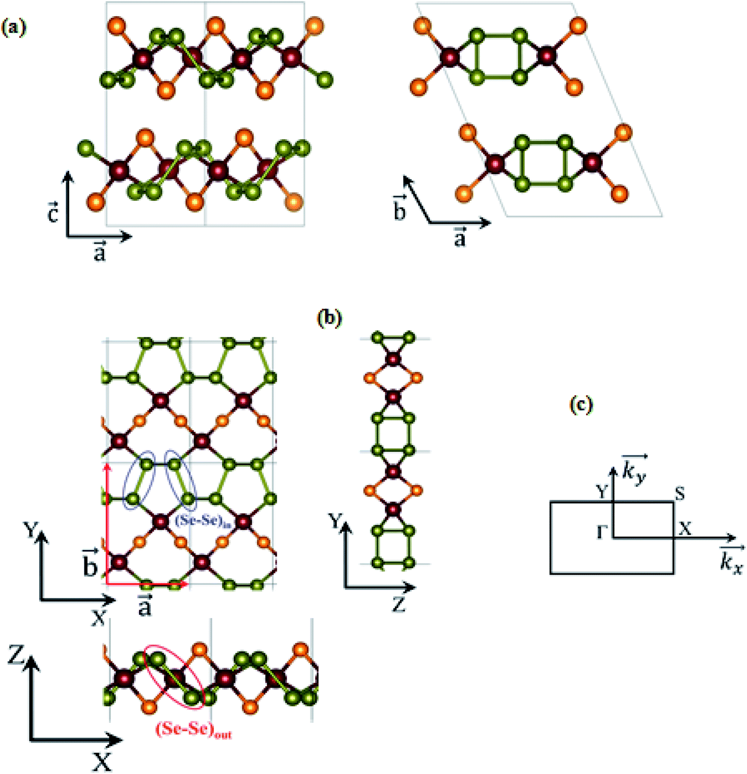 | ||
Fig. 1 Different views of the chemical structures of layered bulk CuXSe2 (a), the CuXSe2 monolayer (b), and the first Brillion zone of CuXSe2 monolayer and points of special symmetry (c). Primitive lattice vectors  and in-plane and out-of-plane Se–Se bonds, (Se–Se)in and (Se–Se)out, are shown. Orange, reddish-brown, and green circles represent halogen (X = Cl, Br), copper (Cu), and selenium (Se) atoms, respectively. and in-plane and out-of-plane Se–Se bonds, (Se–Se)in and (Se–Se)out, are shown. Orange, reddish-brown, and green circles represent halogen (X = Cl, Br), copper (Cu), and selenium (Se) atoms, respectively. | ||
| CuXSe2 | (a, b, c, γ) | dCu–X | dCu–Se | dSe–Sea | dSe–Xb | ∠Se–Se–Se | |
|---|---|---|---|---|---|---|---|
| a The two values correspond to the (Se–Se)in and (Se–Se)out bond lengths, respectively.b Interlayer Se–X distances. | |||||||
| X = Cl | Cal. | (4.87, 7.56, 14.19, 134.78) | 2.289, 2.312 | 2.331, 2.373 | 2.287, 2.579 | 3.42 | 101.4, 104.2 |
| Exp. | (4.63, 7.68, 14.55, 132.79) | — | 2.409, 2.420 | 2.316, 2.393 | 3.19 | 102.9, 104.4 | |
| X = Br | Cal. | (4.88, 7.86, 12.38, 114.53) | 2.427, 2.428 | 2.361, 2378 | 2.339, 2.521 | 3.59 | 103.0, 103.1 |
| Exp. | (4.64, 7.88, 11.18, 103.44) | 2.421, 2.436 | 2.420, 2.436 | 2.339, 2.410 | 3.32 | 102.88, 104.25 | |
To assess the thermodynamic stability of CuXSe2 nanocomposites with respect to the bulk of their constituent partial structures, we calculated the related enthalpies of reaction (ΔrH) using the following equation:
| ΔrH = [E(CuXSe2)bulk − (E(CuX) + 2 × E(S∞))] | (2) |
![[4 with combining macron]](https://www.rsc.org/images/entities/char_0034_0304.gif) 3m space group, No. 216) per formula unit. E(Se∞) represents the total energy of bulk trigonal Se (P3121 space group, No. 151) per atom (the optimized bulk crystal structures of Se, CuCl and CuBr are presented in the ESI†). The calculated reaction energies are −0.37 eV and −0.34 eV for CuClSe2 and CuBrSe2, respectively, confirming the nanocomposites are thermodynamically stable. The calculated values are in good agreement with experimentally obtained data for CuXSe2 (>−0.52 eV).39
3m space group, No. 216) per formula unit. E(Se∞) represents the total energy of bulk trigonal Se (P3121 space group, No. 151) per atom (the optimized bulk crystal structures of Se, CuCl and CuBr are presented in the ESI†). The calculated reaction energies are −0.37 eV and −0.34 eV for CuClSe2 and CuBrSe2, respectively, confirming the nanocomposites are thermodynamically stable. The calculated values are in good agreement with experimentally obtained data for CuXSe2 (>−0.52 eV).39
From bulk to layers
CuXSe2 monolayers were constructed by optimizing the atomic positions and lattice constants of single layers taken from the bulk structures. Both CuClSe2 and CuBrSe2 monolayers are composed of a rectangular primitive cell with a P21 symmetry group (No. 4). As shown in Fig. 1b, the general structural features of the monolayers remain quite similar to those of the bulk structures after optimization. These results were expected based on the nature of the bonding—i.e., weak van der Waals interactions—between the stacked covalent layers. The optimized lattice constants are calculated to be a = 4.84 Å and b = 7.56 Å for CuClSe2 monolayers and a = 4.86 Å and b = 7.70 Å for CuBrSe2 monolayers, which are slightly different from the respective values for the bulk structures.Are the two-dimensional P21 CuXSe2 (X = Cl, Br) structures viable?
To answer to this question, we investigated the thermodynamic, dynamic, mechanical and thermal stabilities of the structures. Note that an assessment of chemical stability, such oxidation processes, was not the purpose of the present study. Thus, we first evaluated the thermodynamic stability of 2D CuXSe2 using the eqn (1) reaction in which the bulk phase is replaced by the 2D structure. The calculated reaction enthalpies at T = 0 K are negative: −0.09 and −0.08 eV per f.u. for the CuClSe2 and CuBrSe2 monolayers, respectively. Next, we quantified the ease of exfoliating CuXSe2 by calculating the cleavage energy of its monolayers and bilayers from the bulk system.The cleavage energy was computed as the energy difference between the ground state energies of (i) a six-layer slab, approximated as a model of the bulk, and (ii) a five (four)-layer slab plus a monolayer (bilayer) separated from the slab. As shown in Fig. 2, the cleavage energies are 0.24 and 0.25 J m−2 for CuClSe2 and CuBrSe2 monolayers, respectively, which are slightly smaller than the cleavage energies calculated for the bilayers (0.25 and 0.26 J m−2). However, the slab method of calculating exfoliation energy has two main disadvantages: (i) it neglects further stabilization of the exfoliated monolayer due to a possible change in lattice constants and (ii) a thick slab is required to obtain reliable results. In 2018, Jung et al.40 proposed an exact, simple method for calculating the exfoliation energy of layered materials. In this method, the n-layer exfoliation energy per unit area (Eexf(n)) is calculated by: Eexf(n) = (Eiso(n) − Ebulk(n/2))/A where Eiso(n) is the energy of a fully optimized isolated n-layer CuXSe2, Ebulk/2 is the energy of the bulk CuXSe2 per layer, and A is the in-plane area of bulk CuXSe2. The calculated Eexf(1) and Eexf(2) values are 0.24 and 0.26 J m−2 for CuClSe2 and 0.23 and 0.22 J m−2 for CuBrSe2, which are slightly different to the values obtained using the slab model. To compare these exfoliation energies with others, we calculated the exfoliation energy of graphene from graphite AB at PBE-D2 level of theory (see Fig. 2). Our calculated value (0.344 J m−2) is in very good agreement with the experimentally obtained value of 0.37 J m−2 and another theoretically predicted value by Jung et al. (0.336 J m−2).40,41 Thus, one may see that the exfoliation energies of 2D CuXSe2 are smaller than the theoretically value for graphene and many other 2D materials (e.g. theoretically predicted exfoliation energies: 0.37 J m−2 for GeS,42 0.63 J m−2 for GeTe,43 and 1.14 J m−2 for GeP344), indicating that monolayer or few-layer CuXSe2 can be easily synthesized using mechanical or liquid-phase exfoliation methods. Our investigation demonstrates that these two-dimensional CuXSe2 compounds could be directly fabricated or exfoliated from their bulk systems as free-standing or suspended monolayers.
 | ||
| Fig. 2 Cleavage energy as a function of separation distance between the CuXSe2 monolayer (bilayer) and five (four)-layer slab. The theoretical PBE-D2 and experimental exfoliation energies of graphene are also shown. | ||
As well as being thermodynamically stable, CuXSe2 monolayers must also be dynamically and mechanically stable to exist. The dynamic stabilities of the monolayers were assessed by calculating their phonon dispersion spectra. As apparent from Fig. 3a and b, zero imaginary frequency is found in the phonon spectrum of the two 2D structures, confirming their dynamic stability. Our detailed analysis of the phonon-projected DOS shows that the highest frequency modes of both monolayers (∼295 and 280 cm−1 for CuClSe2 and CuBrSe2, respectively) contributed almost exclusively from vibration of the Se∞. In addition, the highest frequency modes (∼233 and ∼190 cm−1 for CuClSe2 and CuBrSe2, respectively) correspond to vibration of Cu–Se bonds. These values are close to that of tellurene (∼200 cm−1),45 while appreciably smaller than those of strongly bonded covalent materials like GeP3 (480 cm−1)44 and MoS2 (473 cm−1),46 indicating relatively weak interactions occur between the Se∞ and CuX nanochains.
 | ||
| Fig. 3 Phonon dispersion for CuClSe2 (a) and CuBrSe2 (b) monolayers. | ||
Let us now turn our discussion to the mechanical stability of our proposed 2D crystalline P21 CuXSe2 compounds. A 2D structure with a rectangular primitive cell is mechanically stable if it satisfies the following conditions: C11C22 − C122 > 0 and C66 > 0, where C11, C22, C122 and C66 are the elastic constants.47,48 Within the framework of harmonic approximation, the elastic constants can be determined from a series of parabolic fittings of the strain energy (Es) with respect to uniaxial and biaxial strain. The strain energy of a 2D material is defined as Es = 1/2C11εxx2 + 1/2C22εyy2 + C12εxxεyy + 2C66εxy, where Es, εxx, εyy, and εxy are strain energy per unit area, uniaxial strain along the x and y axes, and shear strain, respectively. The calculated elastic constants for CuClSe2 (C11 = 21.25 N m−1, C22 = 26.81 N m−1, C12 = 6.63 N m−1, and C66 = 9.74 N m−1) and CuBrSe2 (C11 = 12.57 N m−1, C22 = 25.53 N m−1, C12 = 7.68 N m−1, and C66 = 1.92 N m−1) fully satisfy the mechanical stability criteria. To investigate more deeply the mechanical properties of CuXSe2 monolayers, we computed their in-plane stiffnesses (C) and Poisson's ratios (ν) on the basis of the calculated elastic constants. In-plane stiffness along X and Y directions are defined as follows: CX = (C11C22 − C122)/C22 and CY = (C11C22 − C122)/C11. CuClSe2 has comparable stiffness along the X and Y directions (CX = 19.61 and CY = 24.74 N m−1), whereas CuBrSe2 shows highly anisotropic mechanical behavior and is two times softer along the X direction (CX = 10.26 N m−1 and CY = 20.83 N m−1). The stiffness values for the two monolayers are appreciably lower than those of graphene (350 N m−1)49 and MoS2 (127 N m−1).50 The Poisson's ratios (νx = C12/C22, νy = C12/C11) are νx = 0.25 and νy = 0.31 for CuClSe2. However, the Poisson's ratios for CuBrSe2 (νx = 0.30 and νy = 0.61) also show strongly anisotropic behavior. In fact, the large νy value of CuBrSe2 indicates that greater transverse contraction occurs in response to tensile strain along the Y direction than along the X direction. Recall that similar anisotropic Poisson's ratios (νarmchiar = 0.24 and νzigzag = 0.81) and in-plane stiffness (Carmchiar = 26.16 and Czigzag = 88.02 N m−1) were observed for α phosphorene.51
Finally, we checked the thermal stability of 2D CuXSe2 by running ab initio molecular dynamics (AIMD) simulations at 300 and 450 K for 5 ps (see technical details in the ESI†). Note that, experimentally, bulk CuClSe2 melting point is about 601 K.21 As shown in Fig. S1,† the interchain (Cu–Se) and intrachain (Cu–X, Se–Se) bonds remain almost intact, even at temperatures as high as 450 K. The tetrahedral CuX2Se2 and selenium chain motifs persist up to 450 K, confirming the good thermal stabilities of 2D CuXSe2 materials.
Electronic and bonding properties in two-dimensional CuXSe2
Now, we focus our bonding discussion on the prototypical 2D P21 CuClSe2 layer, which is isostructural and isovalent to CuBrSe2. The formal oxidation formalism for CuClSe2 is (Cu+)(Cl−)(Se2). As mentioned previously, the CuClSe2 layer contains two one-dimensional helical Cu2Cl2 and Se4 chains running along the [100] direction with optimized PBE-D2 dihedral angles of 54.76°/56.85° and 32.26°/74.36°, respectively. These inorganic spirals are linked to each other through copper–selenium 2e–2c bonds, leading to five-membered CuSe4 rings. Two-dimensional CuClSe2 contains tetrahedrally coordinated copper atoms—CuCl2Se2 units—and bent Cl ligands. Each Se chain contains bent selenium atoms with alternating short (2.29 Å) and long (2.58 Å) single Se–Se bonds (2.40 Å in pure solid-state Se). These local atomic structural environments can be easily understood from simple electron counting and VSEPR theory. A Lewis structure—one localized bonding picture—of a CuClSe2-based fragment is displayed in Fig. 4. | ||
| Fig. 4 Resonant Lewis structure of a CuCl2Se4 fragment found in the 2D P21 CuClSe2 crystalline structure. The building block, CuClSe2, is highlighted by the blue brackets. The five one pairs of d10 copper are shown in pink, while the 2e metal–ligand bonds are symbolized by arrows. The σ-bond skeleton of the 1D covalent selenium chain is displayed as red lines. VSEPR AXnEm notation is used (A, central atom; X, ligand and n, its number; E, lone pairs and m its number; n + m is the steric number). | ||
A tetrahedral environment is expected for this 18-valence electron CuCl2Se2 unit (d10 Cu+: 10 electrons; two bridging μ-Cl− ligands: 2 × 2 electrons; two R2Se ligands or one bidentate RSe–(Se)2–SeR ligand: 2 × 2 electrons). Along the spiral Se chain, each selenium is bent as expected based on VSEPR rules (AX2E2 center), while the helical form of the covalent Se chain is mainly due to repulsive interactions between the lone pairs located on each Se atom. The electronic structure of this periodical 2D crystalline structure can be understood by starting with an analysis of the orbitals of an isolated d10 tetrahedral CuL4 fragment (L = two-electron donor ligand such as Cl− or Se2−). Let us start with a symmetric molecular model, Td CuCl43− (the charge was chosen to preserve the closed shell configuration corresponding to Cu+ and Cl−); the orbital interaction diagram is shown in Fig. 5. Only the σ orbitals—a pure pσ atomic orbital if s–p mixing is weak (Cl case) or a hybrid sp orbital if not (Se case), as displayed in Fig. 5 on the far right—are taken into account here. One may also consider the π contributions from the ligand—one pπ orbital per sp2 main group atom—though this leads to the same frontier orbitals picture, which has been previously studied by others.52
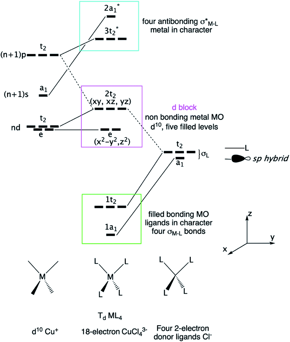 | ||
| Fig. 5 Molecular orbital derivation of the frontier orbitals of a tetrahedral ML4 complex. The CuCl43− fragment with d10 Cu+ and 2-electron Cl− ligands is taken as a model. | ||
First, d orbital splitting is observed, Cu e below Cu t2 – HOMO, which is expected for a tetrahedral complex. The HOMO has significant contributions from the p orbitals of the ligands and the 3d orbitals of Cu, in an out-of-phase combination. Nevertheless, mixing of the Cu 4p orbitals into the HOMO with a Cu–L bonding phase renders the HOMO less antibonding. Thus, the three t2 levels are fully occupied and metallic in character (HOMO) as the two e levels are occupied (d10 configuration). Second, the vacant Cu 4s and 4p atomic orbitals interact strongly with the occupied s and p levels of the ligand, leading to four occupied bonding s levels (a1 + t2) and four unoccupied antibonding levels. As the Cl 3p orbitals are above the 3d Cu AOs, the antibonding LUMO s Cu–L levels are more localized on the chlorine atoms.
Next, in our Td CuL4 model, we replaced the two Cl− ligands with two Se2− atoms, leading to C2v CuCl2Se25−. The frontier orbital character remains: the HOMO is mainly Cu in character; whereas the LUMO is mainly Se (Cl is more electronegative than Se). This is a localized picture of the chemical bonding in extended two-dimensional CuClSe2, highly simplified. Let trace possible electronic structure relationships between these molecular models (localized picture) and the extended net of two-dimensional CuClSe2 (delocalized picture). To do so, the density of states (DOS) of CuClSe2 can be decomposed into Cu, Cl and Se contributions, as illustrated in Fig. 6a. Moreover, chemical bonding analyses were also performed by computing the crystal orbital Hamilton population (COHP),35 which allows identification of bonding and antibonding contributions to the electronic band structure by weighting the off-site projected DOS with the corresponding Hamiltonian matrix elements (hence, negative COHP values denote stabilizing interactions). Thus, integrated COHP (ICOHP) gives a measure of bond strength in the CuClSe2 layers (see Fig. 6a).
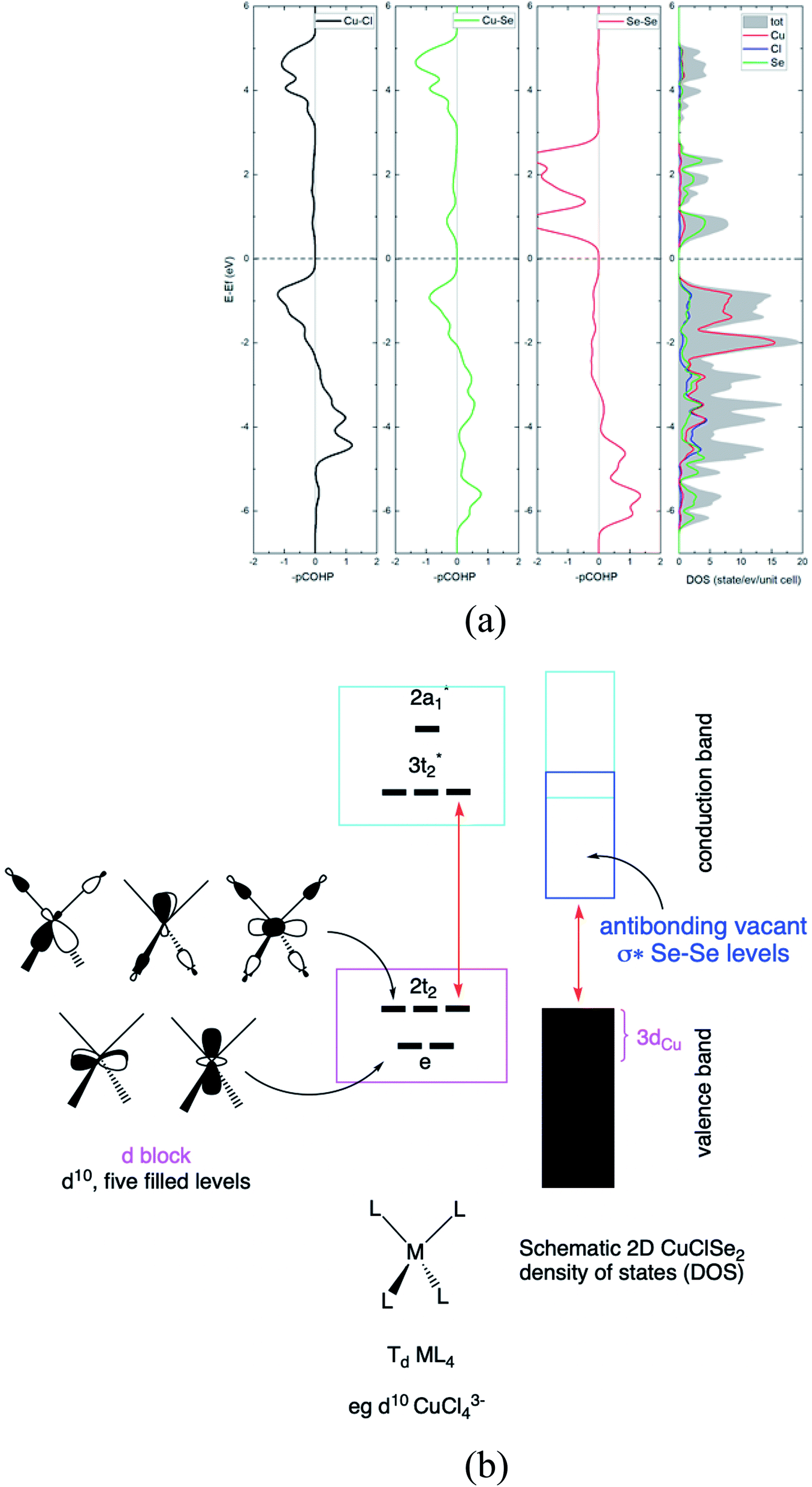 | ||
| Fig. 6 (a) Calculated COHP curves and DOS for two-dimensional P21 CuClSe2. (b) Schematic of the 2D P21 CuClSe2 density of states. The metal MO levels of the isolated d10 tetrahedral ML4 fragment are displayed on the left. | ||
At the top of the valence band, the states are mainly Cu 3d, as expected (e + t2 levels, so called block d based on five filled orbitals, d10). These states are only weakly Cu–Se and Cu–Cl antibonding due to the stabilizing effect of Cu 4p mixing into Cu 3d (see the COHP for Cu–Se and Cu–Cl in Fig. 6a). The DOS for the bottom of the conduction band is mainly Se in character, corresponding to the antibonding Se–Se σ* levels as shown in projected Se–Se COHP curves (Fig. 6a).
The interactions between a Se atom with its two Se neighbors is estimated at −3.67 eV per pair (averaged value; −3.96 eV per pair in elemental P3121 Se), indicative of a stronger covalent character along the single-bonded selenium chains. Here, the computed copper-ligand ICOHP values are −1.62 eV per pair (Cu–Se) and −1.34 eV per pair (Cu–Cl), reflecting rather weaker Cu–L covalent bonding. We calculated the electron localization function (ELF) to obtain more insight into the nature of the Cu–Se/Cl bonds in CuXSe2. ELF can quantitatively distinguish different types of chemical bonds by assigning values in the range of 0 to 1 to each point of real space; generally, regions with ELF values close to 1 indicate strong covalent bonding or lone pair electrons, while lower ELF values correspond to metallic or ionic bonds and low electron density localization. From the ELF counter maps of CuClSe2 and CuBrSe2 shown in ESI Fig. S2,† one can clearly see electrons are strongly localized around the selenium and halogen atoms, as expected from our Lewis structures that assign lone pairs on Se and halogen atoms (see Fig. 4). Finally, Fig. 6b proposed a conceptual and simplified bridge between the molecular tetrahedral ML4 model and extended net of two-dimensional CuClSe2 electronic structures.
What about the metallicity of these two-dimensional materials? With formal d10 ML4 tetrahedra forming the slab, CuXSe2 should be an insulator or, at least, a semiconductor. The band structure and DOS of the 2D material shown in Fig. 7 agree with this statement. A HSE06 indirect gap of ∼1.7 eV is computed between the valence and conduction bands for CuClSe2 (1.73 eV) and CuBrSe2 (1.74 eV). For both materials, the valence band maximum (VBM) is located at the Y point, whereas the conduction band minimum (CBM) lies on the Γ point (see the band structures displayed in Fig. 7). Although Cl atoms are more electronegative than Br atoms, one may wonder why both materials show almost equal band gaps? Our electronic structure analysis shows that for both materials, the VBM is mainly derived from Cu d orbitals, with minor contributions from the p orbitals of Se and X atoms. However, the CBM comes almost exclusively from the valence orbitals of Se atoms. Consequently, Cl and Br have minor contributions to the band edge states, resulting in almost equal band gaps.
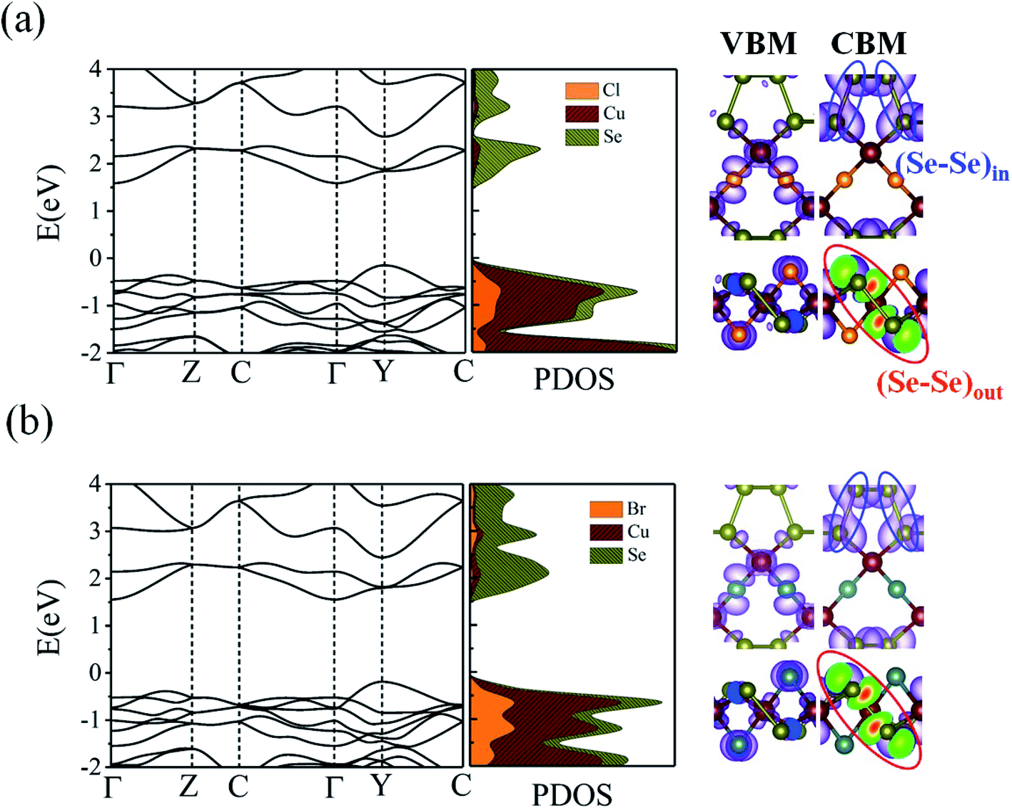 | ||
| Fig. 7 HSE06 band structures and the corresponding partial density of states (PDOS) for (a) CuClSe2 (a) and CuBrSe2 (b) monolayers. The charge density distributions of the VBM and CBM are also shown for each monolayer. | ||
From monolayers to bilayers
We also calculated the electronic band structures of CuXSe2 bilayers to examine the effect of decreasing quantum confinement on the electronic properties of the monolayers. The same stacking pattern used for bulk CuXSe2 was used to construct the bilayers. Fig. 8 shows the HSE06 electronic band structures and charge density distributions of the VBM and CBM for both CuClSe2 and CuBrSe2 bilayers. The bilayers exhibit indirect band gaps of 1.54 and 1.59 eV for CuClSe2 and CuBrSe2, respectively; these values are slightly lower than those of the corresponding monolayers. The decrease in the band gap from mono to bilayer formation is 0.19 eV for CuClSe2 and 0.15 eV for CuBrSe2, appreciably smaller than the change for phosphorene (0.49 eV),53 indicating much weaker quantum confinement effects in CuXSe2. To understand this, we carefully analyzed the charge density distribution in the VBM and CBM of CuXSe2 bilayers. The CBM represents a weak bonding interaction between the CBMs of two layers, while the VBM represents a non-bonding interaction between the VBMs of two layers (Fig. 8). Therefore, the bilayer CBM is more stable compared to the monolayer, while the VBM remains almost unchanged, resulting in slightly smaller band gaps for CuXSe2 bilayers.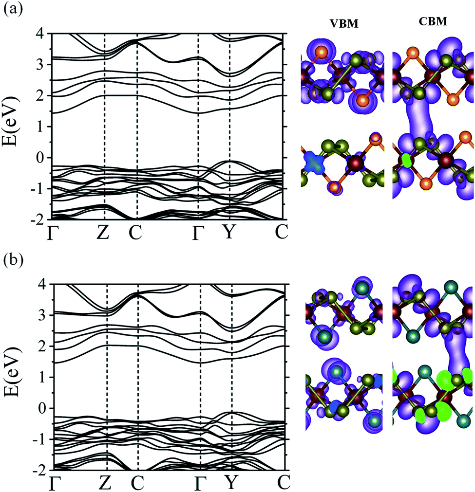 | ||
| Fig. 8 HSE06 band structures of CuClSe2 (a) and CuBrSe2 (b) bilayers. Charge density distributions of the VBM and CBM are also shown for each system. | ||
Carrier mobility of the proposed 2D copper halide selenium materials
Next, we investigated the carrier (electron and hole) mobility of CuXSe2 monolayers along the x and y directions using effective mass approximation and deformation potential theory. In fact, high charge transport in 2D materials has a profound influence on the performance of electronic devices. Table 2 presents the calculated elastic modulus (C2D), effective mass , deformation potential constant (E1j), and carrier mobility (μi) of CuXSe2 monolayers. Both monolayers show extraordinarily anisotropic charge transport along the x and y directions. The electron mobilities along the y direction are 21263.45 and 10274.83 cm2 V−1 s−1 for CuClSe2 and CuBrSe2, respectively, which are ∼768 and 631 times larger than the values along x direction (27.67 and 16.29 cm2 V −1 s−1). However, the opposite trend is observed for hole mobility: the mobilities along the y direction (98.30 and 95.64 cm2 V−1 s−1) are 20 and 9 times smaller than the values along the x direction (2054.21 and 892.61 cm2 V−1 s−1). In other words, electron transport occurs almost exclusively along the y direction, while holes highly favor the x direction. This effectively separates the photo-generated electron–hole pairs, which indicates the monolayers hold promise for application in photovoltaic cells and photocatalysis. The calculated mobilities are in the same range as those of phosphorene (∼10000 cm2 V−1 s−1),53 and appreciably larger than those of other 2D materials like MnPSe3 (∼626 cm2 V−1 s−1)54 and MoS2 (∼200 cm2 V−1 s−1).50 According to Table 2, the anisotropic charge transport mainly originates from the highly direction-dependent deformation potentials for both electrons and holes. Specifically, the E1CBM values along the y direction are 0.16 and 0.23 eV for CuClSe2 and CuBrSe2, respectively, which are about 24 and 17 times smaller than the corresponding values along the x direction (3.74 and 3.85 eV). This observation can be rationalized when one considers that the CBM for both monolayers represents weak (Se–Se)in π bonds along the y direction and (Se–Se)out σ* bonds along the x direction (Fig. 7). Accordingly, we can confidently say that (Se–Se)out σ* bonds are much more sensitive to lattice dilation than weak (Se–Se)in π bonds, which have much larger E1CBM values along x.
 of electrons and holes with respect to the free-electron mass (m0), deformation potential constant of VBM and CBM (E1VBM, E1CBM), and mobility (μe, μh) of electrons and holes along X and Y directions for CuXSe2 monolayers. All parameters were calculated using the HSE06 functionala
| Direction | C2D (J m−2) | Electron | Hole | |||||
|---|---|---|---|---|---|---|---|---|
|
E1CBM (eV) | μe |
|
E1VBM (eV) | μh | |||
| a Mobility at 300 K, cm2 V−1 s−1. | ||||||||
| CuClSe2 | X | 19.61 | 1.30 | 3.737 | 27.673 | 1.17 | 0.588 | 2054.206 |
| Y | 24.74 | 1.23 | 0.155 | 21263.445 |
0.81 | 3.644 | 98.298 | |
| CuBrSe2 | X | 10.26 | 1.22 | 3.850 | 16.289 | 1.47 | 0.558 | 892.608 |
| Y | 20.83 | 1.22 | 0.229 | 10274.830 |
0.73 | 3.620 | 95.645 | |

Optical performance of CuXSe2 monolayers
Their good stability, ease of exfoliation, moderate band gap and extraordinary anisotropic charge transport make CuXSe2 monolayers promising potential candidates for optoelectronics applications. Thus, we examined the optical performance of CuXSe2 monolayers by calculating their frequency-dependent complex dielectric constants using the HSE06 method. As shown in Fig. 9, the monolayers obviously absorb light over a broad range of the visible spectrum (2 to 3.2 eV). The monolayers also show anisotropic absorbance coefficients, similarly to phosphorene. In spite of their indirect band gaps, the calculated absorbance coefficients (>105 cm−1) are comparable to those of hybrid halide perovskites, which are highly efficient light harvesting materials employed in solar cells.55,56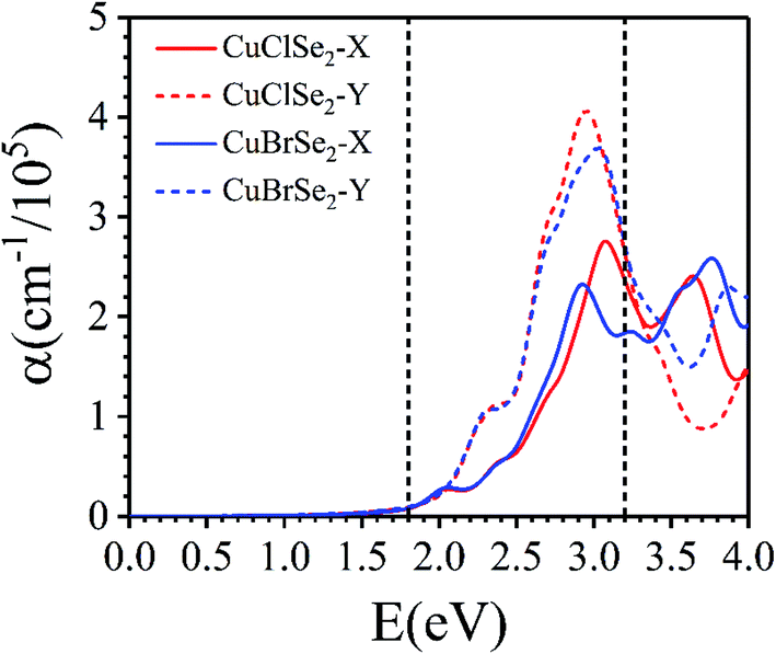 | ||
| Fig. 9 Frequency-dependent absorption coefficients of CuXSe2 monolayers. The energy range corresponding to visible light is indicated by vertical dashed lines. | ||
Strain effects
We also examined the effect of strain on the electronic band structure of CuXSe2 monolayers. We only focused on biaxial tensile strain up to 8%, as compression is barely achievable experimentally. The strain energies at 8% are 50 meV per atom for CuClSe2 and 44 meV per atom for CuBrSe2, slightly larger than the thermal energy at room temperature (25 meV per atom), indicating its energetically feasible. Fig. 10 shows the band gap initially increases as strain increases for both monolayers, reaching maximums of 1.90 eV for CuClSe2 and 1.83 eV for CuBrSe2 at 4%, and then decreases at 8% to 1.60 eV for CuClSe2 and 1.49 eV for CuBrSe2. The nature of the band gap also sensitively responds to strain, as each monolayer experiences indirect–direct–indirect band gap transitions (Fig. 11). The gap remains indirect up to 3%, while the CBM moves from Γ-point to Y-point at 4%, resulting in an indirect-to-direct band gap transition. Moreover, at 5%, the VBM moves to Z′, which lies on the Z → Γ path, again transforming the monolayers to indirect band gap semiconductors.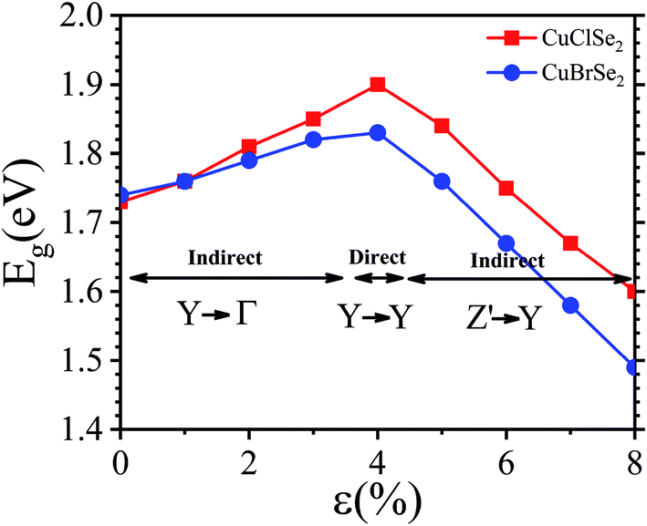 | ||
| Fig. 10 Band gap variation of the CuXSe2 monolayers as a function of biaxial strain. | ||
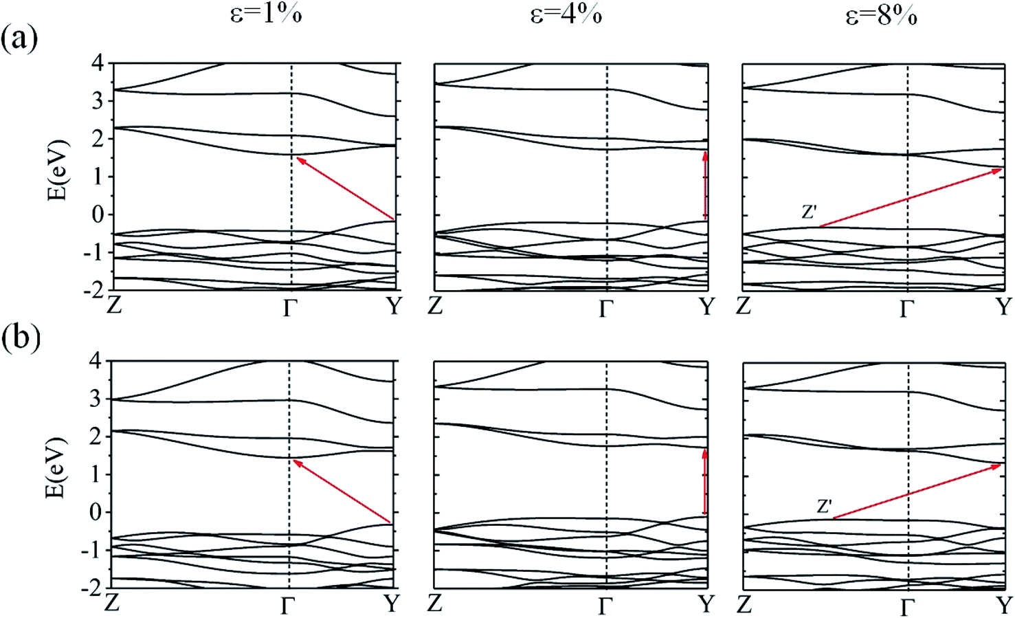 | ||
| Fig. 11 The HSE06 band structures of CuClSe2 (a) and CuBrSe2 (b) under 1%, 4% and 8% biaxial tensile strain. | ||
4. Conclusion
We systematically investigated the structural, mechanical, electronic and optical properties of CuXSe2 (X = Cl, Br) nanocomposite monolayers and bilayers using first-principles DFT calculations. Exfoliation from CuXSe2 (X = Cl, Br) layered bulk phases is computationally feasible based on the small cleavage energies. In addition, the phonon spectrum, calculated elastic constants and AIMD simulations suggest freestanding 2D CuXSe2 (X = Cl, Br) are dynamically, mechanically and thermodynamically stable. The monolayers are indirect-gap semiconductors with practically the same band gaps (1.73 eV for CuClSe2 and 1.74 eV for CuBrSe2) and exhibit extremely anisotropic and very high carrier mobilities. We found that intrinsic charge transport in CuXSe2 is almost exclusively unidirectional for electrons and holes (i.e., electron mobilities are 21263.45 and 10274.83 cm2 V−1 s−1 along the y direction for CuClSe2 and CuBrSe2, respectively, while hole mobilities are 2054.21 and 892.61 cm2 V−1 s−1 along the x direction). These results indicate very good separation of photogenerated electron–hole pairs. CuXSe2 bilayers are also indirect band gap semiconductors with slightly smaller band gaps of 1.54 and 1.59 eV for CuClSe2 and CuBrSe2, respectively, suggesting weak interlayer quantum confinement effects. On the other hand, CuXSe2 monolayers have high absorption coefficients (>105 cm−1) over a wide range of the visible light spectrum. Their moderate band gaps, very high unidirectional electron and hole mobilities, and high absorption coefficients indicate the proposed CuXSe2 (X = Cl, Br) nanocomposite monolayers hold promise for applications in optoelectronic devices.
Conflicts of interest
There are no conflicts to declare.Acknowledgements
The authors thank Shahid Chamran University of Ahvaz, the School of Nanoscience, Institute for Research in Fundamental Sciences (IPM), CNRS and Nouvelle Aquitaine Region – FEDER for supporting this scientific research. This research was partially supported by the Research Council of Shahid Chamran University of Ahvaz (GN 1398), the Center for International Scientific & Collaboration (CISSC) Ministry of Science Research and Technology, the Hubert Curien Partnership PHC Gundishapur 2019 (No. 42961 PF, PI G. F.) and PRCI ANR Predict_2D_NanoMat (PI G. F.). We also acknowledge the High-Performance Computing Centers of Poitiers University (Mesocentre SPIN) and the GENCI (TGCC/Irene and CINES/Occigen, France) under Project No. X2016087539 for allocation of computing time.References
- K. S. Novoselov, A. K. Geim, S. V. Morozov, D. Jiang, Y. Zhang, S. V. Dubonos, I. V. Grigorieva and A. A. Firsov, Science, 2004, 306, 666–669 CrossRef CAS PubMed.
- A. K. Geim and K. S. Novoselov, Nat. Mater., 2007, 6, 183–191 CrossRef CAS PubMed.
- Q. H. Wang, K. Kalantar-Zadeh, A. Kis, J. N. Coleman and M. S. Strano, Nat. Nanotechnol., 2012, 7, 699–712 CrossRef CAS PubMed.
- L. Li, Y. Yu, G. J. Ye, Q. Ge, X. Ou, H. Wu, D. Feng, X. H. Chen and Y. B. Zhang, Nat. Nanotechnol., 2014, 9, 372–377 CrossRef CAS PubMed.
- Y. Zheng, Y. Jiao, L. Ge, M. Jaroniec and S. Z. Qiao, Angew. Chem., Int. Ed., 2013, 52, 3110–3116 CrossRef CAS PubMed.
- M. A. Lukowski, A. S. Daniel, F. Meng, A. Forticaux, L. Li and S. Jin, J. Am. Chem. Soc., 2013, 135, 10274–10277 CrossRef CAS PubMed.
- S. Yang, Y. Gong, J. Zhang, L. Zhan, L. Ma, Z. Fang, R. Vajtai, X. Wang and P. M. Ajayan, Adv. Mater., 2013, 25, 2452–2456 CrossRef CAS PubMed.
- K. S. Kumar, N. Choudhary, Y. Jung and J. Thomas, ACS Energy Lett., 2018, 3, 482–495 CrossRef CAS.
- K.-S. Chen, I. Balla, N. S. Luu and M. C. Hersam, ACS Energy Lett., 2017, 2, 2026–2034 CrossRef CAS.
- X. Li and L. Zhi, Chem. Soc. Rev., 2018, 47, 3189–3216 RSC.
- H. Liu, A. T. Neal, Z. Zhu, Z. Luo, X. Xu, D. Tománek and P. D. Ye, ACS Nano, 2014, 8, 4033–4041 CrossRef CAS PubMed.
- A. J. Mannix, B. Kiraly, M. C. Hersam and N. P. Guisinger, Nat. Rev. Chem., 2017, 1, 0014–14 CrossRef CAS.
- F. Wang, T. A. Shifa, P. Yu, P. He, Y. Liu, F. Wang, Z. Wang, X. Zhan, X. Lou, F. Xia and J. He, Adv. Funct. Mater., 2018, 28, 1802151–1802224 CrossRef.
- T. L. Tan, H. M. Jin, M. B. Sullivan, B. Anasori and Y. Gogotsi, ACS Nano, 2017, 11, 4407–4418 CrossRef CAS PubMed.
- T. Gao, Q. Zhang, L. Li, X. Zhou, L. Li, H. Li and T. Zhai, Adv. Opt. Mater., 2018, 6, 1800058–1800073 CrossRef.
- A. Rabenau and H. Rau, Solid State Commun., 1969, 7, 1281–1282 CrossRef CAS.
- W. Milius and A. Rabenau, Z. Naturforsch. B Chem. Sci., 1988, 43, 243–244 CAS.
- A. Pfitzner, T. Nilges and H.-J. Deiseroth, Z. Anorg. Allg. Chem., 1999, 625, 201–206 CrossRef CAS.
- J. Fenner, Acta Crystallogr., Sect. B: Struct. Crystallogr. Cryst. Chem., 1976, 32, 3084–3086 CrossRef.
- W. Milius, Z. Naturforsch. B Chem. Sci., 1989, 44, 990–992 CAS.
- Y. Wang, Z. Deng, X. Lv, F. Miao, S. Wan, X. Fang, Q. Zhang and S. Yin, Mater. Lett., 2009, 63, 236–238 CrossRef CAS.
- Y.-Q. Liu, H.-D. Wu, Y. Zhao and G.-B. Pan, RSC Adv., 2014, 4, 45844–45847 RSC.
- G. Kresse and D. Joubert, Phys. Rev. B: Condens. Matter Mater. Phys., 1999, 59, 1758–1775 CrossRef CAS.
- G. Kresse and J. Hafner, Phys. Rev. B: Condens. Matter Mater. Phys., 1993, 47, 558–561 CrossRef CAS PubMed.
- G. Kresse and J. Furthmuller, Phys. Rev. B: Condens. Matter Mater. Phys., 1996, 54, 11169–11186 CrossRef CAS PubMed.
- J. P. Perdew, K. Burke and M. Ernzerhof, Phys. Rev. Lett., 1996, 77, 3865–3868 CrossRef CAS PubMed.
- S. Grimme, J. Comput. Chem., 2006, 27, 1787–1799 CrossRef CAS PubMed.
- A. V. Krukau, O. A. Vydrov, A. F. Izmaylov and G. E. Scuseria, J. Chem. Phys., 2006, 125, 224106–224110 CrossRef PubMed.
- L. Chaput, A. Togo, I. Tanaka and G. Hug, Phys. Rev. B: Condens. Matter Mater. Phys., 2011, 84, 094302–094306 CrossRef.
- A. Togo, F. Oba and I. Tanaka, Phys. Rev. B: Condens. Matter Mater. Phys., 2008, 78, 134106–134109 CrossRef.
- S. Nose, J. Chem. Phys., 1984, 81, 511–519 CrossRef CAS.
- S. Nose, Prog. Theor. Phys. Suppl., 1991, 103, 1–46 CrossRef CAS.
- D. M. Bylander and L. Kleinman, Phys. Rev. B: Condens. Matter Mater. Phys., 1992, 46, 13756–13761 CrossRef PubMed.
- J. Bardeen and W. Shockley, Phys. Rev., 1950, 80, 72–80 CrossRef CAS.
- R. Dronskowski and P. E. Bloechl, J. Phys. Chem., 1993, 97, 8617–8624 CrossRef CAS; S. Maintz, V. L. Deringer, A. L. Tchougreeff and R. Dronskowski, J. Comput. Chem., 2013, 34, 2557–2567 CrossRef PubMed.
- R. Hoffmann, J. Chem. Phys., 1963, 39, 1397–1412 CrossRef CAS.
- C. Mealli and D. M. Proserpio, J. Chem. Educ., 1990, 67, 399–402 CrossRef CAS.
- K. Momma and F. Izumi, J. Appl. Crystallogr., 2008, 41, 653–658 CrossRef CAS.
- A. Rabenau, H. Rau and G. Rosenstein, Z. Anorg. Allg. Chem., 1970, 374, 43–53 CrossRef CAS.
- J. H. Jung, C.-H. Park and J. Ihm, Nano Lett., 2018, 18, 2759–2765 CrossRef CAS PubMed.
- W. Wang, S. Dai, X. Li, J. Yang, D. J. Srolovitz and Q. Zheng, Nat. Commun., 2015, 6, 7853–7859 CrossRef CAS PubMed.
- F. Li, X. Liu, Y. Wang and Y. Li, J. Mater. Chem. C, 2016, 4, 2155–2159 RSC.
- M. Qiao, Y. Chen, Y. Wang and Y. Li, J. Mater. Chem. A, 2018, 6, 4119–4125 RSC.
- Y. Jing, Y. Ma, Y. Li and T. Heine, Nano Lett., 2017, 17, 1833–1838 CrossRef CAS PubMed.
- Z. Zhu, X. Cai, S. Yi, J. Chen, Y. Dai, C. Niu, Z. Guo, M. Xie, F. Liu, J.-H. Cho, Y. Jia and Z. Zhang, Phys. Rev. Lett., 2017, 119, 106101–106105 CrossRef PubMed.
- A. Molina-Sánchez and L. Wirtz, Phys. Rev. B: Condens. Matter Mater. Phys., 2011, 84, 155413–155418 CrossRef.
- S. Zhang, J. Zhou, Q. Wang, X. Chen, Y. Kawazoe and P. Jena, Proc. Natl. Acad. Sci. U. S. A., 2015, 112(8), 2372–2377 CrossRef CAS PubMed.
- Y. Wang, F. Li, Y. Li and Z. Chen, Nat. Commun., 2016, 7, 11488–11494 CrossRef CAS PubMed.
- T. Jiang, R. Huang and Y. Zhu, Adv. Funct. Mater., 2014, 24, 396–402 CrossRef CAS.
- Y. Cai, G. Zhang and Y.-W. Zhang, J. Am. Chem. Soc., 2014, 136, 6269–6275 CrossRef CAS PubMed.
- M. Elahi, K. Khaliji, S. M. Tabatabaei, M. Pourfath and R. Asgari, Phys. Rev. B: Condens. Matter Mater. Phys., 2015, 91, 115412–115418 CrossRef.
- T. A. Albright, J. K. Burdett and M.-H. Whangbo, Orbital Interactions in Chemistry, Wiley, 2nd edn, 2013, ISBN: 9780471080398 Search PubMed.
- J. Qiao, X. Kong, Z.-X. Hu, F. Yang and W. Ji, Nat. Commun., 2014, 5, 4475–4484 CrossRef CAS PubMed.
- X. Zhang, X. Zhao, D. Wu, Y. Jing and Z. Zhou, Adv. Sci., 2016, 3, 1600062–1600065 CrossRef PubMed.
- M. Shirayama, H. Kadowaki, T. Miyadera, T. Sugita, M. Tamakoshi, M. Kato, T. Fujiseki, D. Murata, S. Hara, T. N. Murakami, S. Fujimoto, M. Chikamatsu and H. Fujiwara, Phys. Rev. Appl., 2016, 5, 014012–014025 CrossRef.
- G. Mannino, A. Alberti, I. Deretzis, E. Smecca, S. Sanzaro, Y. Numata, T. Miyasaka and A. L. Magna, J. Phys. Chem. C, 2017, 121, 7703–7710 CrossRef.
Footnote |
| † Electronic supplementary information (ESI) available. See DOI: 10.1039/c9ra10380e |
| This journal is © The Royal Society of Chemistry 2020 |